Hexagonal Indium Double Layer on Si(111)-(
Abstract
Density-functional calculations are used to verify the atomic structure of the hexagonal In/Si(111)-() surface, which has been considered to represent an ultimate two-dimensional (2D) limit of metallic In overlayers. Contrary to the prevailing assumption, this surface consists of not a single layer but a double layer of In atoms, which corresponds to a hexagonal deformation of the well-established In double layer formed on Si(111)-() [Park ., Phys. Rev. Lett. 109, 166102 (2012)]. The same double-layer thickness accounts well for the typical coexistence of the hexagonal and rectangular phases and their similar 2D electronic structures. It is thus conclusive that, regardless of rectangular or hexagonal, the In/Si(111)-() surface does not represent an one-atom-thick In overlayer.
pacs:
68.43.Fg, 68.47.Fg, 73.20.AtOne-atom-thick metal overlayers grown on semiconductor surfaces have attracted great attention as model systems ideal for exploring intriguing low-dimensional metallic properties carp96 ; yeom99 ; qin09 ; kim10 ; kwon14 . One representative system of recent interest is the In/Si(111)-() surface, where the In overlayer was generally assumed to be one atom thick surn95 ; kraf95 ; kraf97 and so represent an ideal two-dimensional (2D) limit of metallic In properties. Fascinating electronic features of the In overlayer, including a nearly-free-electron Fermi surface, rote03 , superconducting transitions zhan10 ; uchi11 , and an intriguing metallic transport behavior yama11 , have been explored and referred to as revealing the ultimate 2D limit. With little structural information about the In overlayer, however, its actual layer thickness has long been an open question.
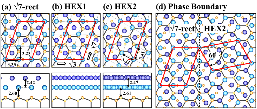
Particularly interesting in this regard is a double-layer picture for the In/Si(111)-() surface, contrary to the prevailing single-layer assumption. In a recent density-functional theory (DFT) study park12 , of the two different In-derived () phases distinguishable in scanning tunneling microscopy (STM) experiments surn95 ; kraf95 ; kraf97 , the more representative, rectangular phase (hereafter, -rect) was verified to contain an In double layer [see Fig. 1(a)]. Consequently, the remaining hexagonal phase (-hex) has been spotlighted as a single-layer alternative, because it typically developes a little earlier than the -rect phase when prepared by In deposition on the Si(111)-(77) surface at about 400 ∘C kraf95 ; kraf97 . Since the -hex phase evolves between the 41 and -rect phases in the coverage-dependent growth process kraf97 ; yama13 , its In coverage would be in between 1.0 ML of the 41 phase bunk99 ; cho01 and 2.4 ML of the -rect phase park12 (here, 1 ML refers to one In atom per surface Si), but the In coverage and thickness is yet to resolve.
In early STM studies, Kraft suggested a 1.0 ML single-layer model for the -hex phase kraf95 ; kraf97 , where the observed five STM protrusions per () unit cell were attributed to five In atoms (corresponding to 1 ML). This experimental model was more quantified by Shang in a recent DFT study shan12 . Another single-layer model with an In coverage of 1.2 ML was lately proposed by Uchida uchi13a , based on a similarity of their DFT simulations to the experimental STM image kraf95 . The In coverage itself is also a matter of debate as seen in two recent experiments: while Uchihashi uchi13 supported the 1.2 ML single-layer model of Uchida uchi13a based on the similarity of STM images, Yamada yama13 estimated as about 2 ML in their reflection high-energy electron diffraction (RHEED) study. Any single-layer model, however, has an inherent experimental problem: in their STM study, Kraft . observed that the coexisting -hex and -rect phases have almost the same STM heights (with a small difference by 0.1–0.2 Å) and also show very similar electron tunneling spectra kraf95 . Previously, these similarities were argued to ensure that both phases have a single In layer kraf95 , but now the recent double-layer verification of the -rect phase park12 should imply a double-layer model for the -hex phase as well.
Here, we propose a new structural model for the hexagonal In/Si(111)-() surface. This model features a double layer of 2.4 ML In atoms, which actually corresponds to a hexagonal deformation of the In double layer of the -rect phase. In what follows, the soundness of the hexagonal double-layer model is demonstrated by DFT calculations.
We perform DFT calculations using the Vienna - simulation package within the generalized gradient approximation perd91 and the projector augmented wave method bloc94 ; Kres96 . The Si(111) surface is modeled by a periodic slab geometry with six atomic layers and a vacuum spacing of about 12 Å. The calculated value 2.370 Å is used as the bulk Si-Si bond length. Indium atoms are adsorbed on the top of the slab, and the bottom is passivated by H atoms. The electronic wave functions are expanded in a plane-wave basis with a kinetic energy cutoff of 246 eV. A 461 -point mesh is used for the () Brillouin-zone integrations. All atoms but the bottom two Si layers are relaxed until the residual force components are within 0.01 eV/Å.
In light that the -hex and -rect phases have similar STM heights kraf95 , we examine first the possibility of hexagonal deformations of the double-layer -rect phase. Figure 1 shows two easy-to-derive hexagonal models. One is obtained from the -rect phase by a monoclinic deformation of the rectangular In array along the direction, as captured in Fig. 1(b) (hereafter, HEX1). The other (HEX2) is obtained from HEX1 by a monoclinic deformation along the direction as shown in Fig. 1(c). In our calculations, while HEX2 is locally stable, HEX1 is unstable and relaxes back to the -rect phase with no energy barrier. We also examined variants of HEX1 and HEX2 by allowing lateral displacements of In atoms along the or direction, but all of them were found to converge to either the -rect phase or the HEX2 model. Figure 1(c) shows the optimized HEX2 structure, which forms almost a regular In lattice ( = 3.23 Å and = 3.41 Å): the In-In and In-Si interlayer spacings are 2.47 Å and 2.61 Å in average, respectively, comparing well with the values, 2.42 Å and 2.60 Å, of the -rect model. In energetics, the HEX2 model is as stable as the -rect model with a slightly higher formation energy by 0.05 eV per () cell, being a promising model for the -hex phase.
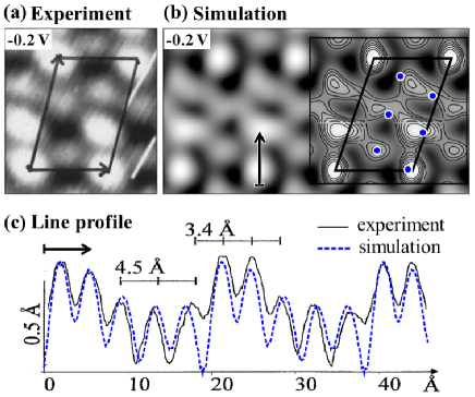
Figure 2 shows the simulated STM image of the HEX2 model, which indeed compares well with the experimental feature of two bright and three weak spots per unit cell kraf97 . In our simulation, two of the three weak spots represent the In-In bonding states rather than individual In atoms, thus accounting for the five (not six) protrusions from six surface In atoms per unit cell. In Fig. 2(c), the calculated charge corrugation is in quantitative agreement with the STM line profile Kraf97 : the maximum height difference between the peaks (0.23 Å) and the interval of the two highest peaks (3.32 Å) compare well with the experimental values of 0.25 Å and 3.4 Å, respectively.
It is interesting to compare the topographic heights of the HEX2 model and the -rect phase. When simulated at a same bias voltage and charge density, the HEX2 model appears lower by 0.24 Å than the -rect model, in good agreement with the STM observation that the -hex phase appears a little lower by 0.1–0.2 Å kraf95 . On the other hand, the 1.2 ML single-layer model of Uchida uchi13 was found to appear far lower by 2.21 Å.
Figure 1(d) displays another fascinating feature of the HEX2 model: it could form an atomically sharp phase boundary with the coexisting -rect phase. This boundary matching is achieved by a 60 ∘ clockwise rotation of the HEX2 model in Fig. 1(c). The resulting angular relation matches well the STM observation that, when the -hex and -rect phases coexist, the angle difference of their unit cells is 60∘ kraf95 ; kraf97 . Their typical coexistence kraf95 is also explained by the aforementioned energetics: since the HEX2 and -rect phases are energetically comparable, both phases would locally develope during the In deposition at high temperatures.
The HEX2 model, consisting of a quasihexagonal In double layer, is not only energetically stable but also reveals sufficiently sound STM features, so we readily propose it as the long-sought structural model for the -hex phase and further explore its electronic structure.
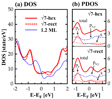
Figure 3 shows the calculated density of states (DOS) of our -hex model. Noticeable is that the -hex model reveals almost the same DOS spectrum as the -rect model, well reflecting their common structural nature (i.e., the same In coverage of 2.4 ML and similar double-layer structures), while the 1.2 ML single-layer model of Uchida uchi13 does not. Our -hex model is thus compatible with the experimental report that the -hex and -rect phases reveal similar scanning tunneling spectra kraf95 . There is of course a little difference in the DOS curves, reflecting the underlying structural difference: the small peak at 0.28 eV in the -rect model is a little shifted up to 0.53 eV in the -hex model. As seen in Fig. 3(b), the difference stems from the and orbitals since their lateral interactions are the most affected by the in-plane rectangular-to-hexagonal deformation.
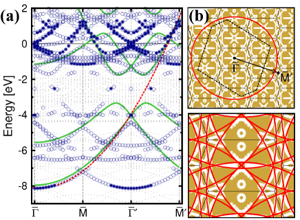
Figure 4 shows the band structure of the -hex model. It is metallic with a broad distribution of In-derived states. Interestingly, the In band structure could be traced from those of the (11) freestanding In double layer [mentioned in Fig. 1(c)]: the () zone folding of this (11) result accounts well for the complicated In bands and the band gap between 3.36 eV and 1.75 eV of the -hex phase. A parabolic fitting (with an effective mass of 0.92 ) connects well the In states from the bottom at 8.13 eV to over the Fermi level. These free-electron-like states were found evenly distributed on both of the top and second In layers (not shown here), implying that the double-layer unit may be essential for the 2D free-electron nature. This surface has similar parabolic bands along other directions, thereby leading to a circular Fermi surface: Its radii are 1.39 and 1.36 along the and directions, respectively. Figure 4(b) shows the large Fermi circle in the extended () Brillouin zones, and the actual Fermi contours are mostly accounted for by the the () zone folding of the large Fermi circle, as seen in the bottom panel. This 2D free-electron nature of the -hex phase is similar to that of the -rect phase: in our calculations, the -rect phase has the band bottom of 8.18 eV, the effective mass of 0.95 , and the Fermi circle of 1.4 .
It is worth mentioning that there is one more () hexagonal phase, differing from the present -hex phase prepared at high temperatures (HT) of about 400 ∘C kraf95 ; kraf97 . Saranin sara06 obtained a hexagonal In/Si(111)-() phase by room-temperature (RT) In deposition on In/Si(111)-() and identified it with the HT -hex phase on the basis of similar STM images. This identification, however, is open to questions. First, the STM comparison of both phases was not fairly done: the RT phase was examined at high biases of 0.5 V and 2 V sara06 , while the HT phase at as low as -0.2 V and -0.12 V kraf97 . Indeed, when taken at about 2 V, our STM simulations for the -hex model do not reproduce the STM image of the RT -hex surface. Second, the RT and HT -hex phases appear differently in topographic height. The HT phase appears higher by about 2.0 Å in STM topograph than the reference () phase kraf95 whereas the RT phase shows only a small height difference of 0.5 Å as found in a recent atomic-force microscopy image iwat13 , which is a strong implication of different -hex phases. Finally, the RT phase has a metastable nature: it transforms into a () phase during cooling in the range from 265 to 225 K sara06 , while the HT phase is stable at cryogenic temperatures as observed in superconductivity experiments uchi11 ; yama13 . Thus, as a metastable intermediate phase, the RT phase should be distinguished from the stable HT phase.
In summary, we proposed a double-layer structural model for the hexagonal In/Si(111)-() surface, based on the quantitative microscopic and spectroscopic examinations by DFT calculations. This double-layer thickness with the In coverage of 2.4 ML is the common structural feature underlying the typical coexistence of the hexagonal and rectangular phases and their similar electronic structures close to a 2D free-electron gas. Therefore, the In/Si(111)-() surface, either rectangular or hexagonal, does not represent a single-layer limit of metallic In overlayers: such an ultimate 2D limit is yet to achieve.
This work was supported by the National Research Foundation of Korea (Grant No. 2011-0008907). The authors acknowledge useful discussions with Tae-Hwan Kim and Han Woong Yeom.
References
- (1) J. M. Carpinelli, H. H. Weitering, E. W. Plummer, and R. Stumpf, Direct observation of a surface charge density wave, Nature 381, 398 (1996)
- (2) H. W. Yeom, S. Takeda, E. Rotenberg, I. Matsuda, J. Schaefer, C. M. Lee, S. D. Kevan, T. Ohta, T. Nagao, and S. Hasegawa, Instability and charge density wave of metallic quantum chains on a silicon surface, Phys. Rev. Lett. 82, 4898 (1999)
- (3) S. Qin, J. Kim, Q. Niu, and C.-K. Shih, Superconductivity at the two-dimensional limit, Science 324, 1314 (2009)
- (4) K. S. Kim, S. C. Jung, M. H. Kang, and H. W. Yeom, Nearly massless electrons in the silicon interface with a metal film, Phys. Rev. Lett. 104, 246803 (2010)
- (5) S. G. Kwon and M. H. Kang, Identification of the Au coverage and structure of the Au/Si(111)-() surface, Phys. Rev. Lett. 113, 086101 (2014)
- (6) S. L. Surnev, J. Kraft, and F. P. Netzer, Modification of overlayer growth kinetics by surface interlayers: The Si(111)- indium surface, J. Vac. Sci. Technol. A 13, 1389 (1995)
- (7) J. Kraft, S. L. Surnev, and F. P. Netzer, The structure of the indium-Si(111)() monolayer surface, Surf. Sci. 340, 36 (1995)
- (8) J. Kraft, M. G. Ramsey, and F. P. Netzer, Surface reconstructions of In on Si(111), Phys. Rev. B 55, 5384 (1997)
- (9) E. Rotenberg, H. Koh, J. Rossnagel, H. W. Yeom, J. Sha:fer, B. Krenzer, M. P. Rocha, and S. D. Kevan, Indium on Si(111): A nearly free electron metal in two dimensions, Phys. Rev. Lett. 91, 246404 (2003)
- (10) T. Zhang, P. Cheng, W.-J. Li, U.-J. Sun, G. Wang, X.-G. Zhu, K. He, L. Wang, X. Ma, X. Chen, Y. Wang, Y. Liu, H.-Q. Lin, J.-F. Jia and Q.-K. Xue, Superconductivity in one-atomic-layer metal films grown on Si(111), Nature Phys. 6, 104 (2010)
- (11) T. Uchihashi, P. Mishra, M. Aono and T. Nakayama, Macroscopic superconducting current through a silicon surface reconstruction with indium adatoms: Si(111)-()-In, Phys. Rev. Lett. 107, 207001 (2011)
- (12) S. Yamazaki, Y. Hosomura, I. Matsuda, R. Hobara, T. Eguchi, Y. Hasekawa, and S. Hasegawa, Metallic Transport in a monatomic layer of In on a silicon surface, Phys. Rev. Lett. 106, 116802 (2011)
- (13) J. W. Park, and M. H. Kang, Double-layer In structural model for the In/Si(111)- surface, Phys. Rev. Lett. 109, 166102 (2012)
- (14) M. Yamada, T. Hirahara, and S. Hasegawa, Magnetoresistance measurements of a superconducting surface state of In-induced and Pb-induced structures on Si(111), Phys. Rev. Lett. 110, 237001 (2013)
- (15) O. Bunk, G. Falkenberg, J. H. Zeysing, L. Lottermoser, R. L. Johnson, M. Nielsen, F. Berg-Rasmussen, J. Baker, and R. Feidenhas’l, Structure determination of the indium-induced Si(111)-() reconstruction by surface x-ray, Phys. Rev. B 59, 12228 (1999)
- (16) J.-H. Cho, D.-H. Oh, K. S. Kim, and L. Kleinman, Weakly correlated one-dimensional indium chains on Si(111), Phys. Rev. B 64, 235302 (2001)
- (17) B. Shang, L-F. Yuan, and J-L. Yang, First-principles study of geometric and electronic structures of Si(111)--In surface reconstruction, Chin. J. Chem. Phys. 25, 403 (2012)
- (18) K. Uchida and A. Oshiyama, Identification of metallic phases of In atomic layers on Si(111) surfaces, Phys. Rev. B 87, 165433 (2013)
- (19) T. Uchihashi, P. Mishra and T. Nakayama, Resistive phase transition of the superconducting Si(111)-()-In surface, Nano. Res. Lett. 8, 167 (2013)
- (20) J. P. Perdew, in Electronic Structure of Solids ’91, edited by P. Ziesche, and H. Eschrig (Akademie Verlag, Berlin, 1991)
- (21) P. E. Blochl, Projector augmented-wave method, Phys. Rev. B 50, 17953 (1994)
- (22) G. Kresse and J. Furthmüller, Efficient iterative schemes for total-energy calculations using a plane-wave basis set, Phys. Rev. B 54, 11169 (1996)
- (23) J. Kraft, M. G. Ramsey, and F. P. Netzer, Strain relief, close-packed overlayer formation and discommensurate phases: In on Si(111), Surf. Sci. 372, L271 (1997)
- (24) A. A. Saranin, A. V. Zotov, M. Kishida, Y. Murata, S. Honda, M. Katayama, K. Oura, D. V. Gruznev, A. Visikovskiy, and H. Tochihara, Reversible phase transitions in the pseudomorphic -hex In layer on Si(111), Phys. Rev. B 74, 035436 (2006)
- (25) K. Iwata, S. Yamazaki, Y. Tani, and Y. Sugimoto, Mechanical properties of various phases on In/Si(111) surfaces revealed by atomic force microscopy, Appl. Phys. Exp. 6, 055201 (2013)