Effect of electron–phonon interaction on the formation of one-dimensional electronic states in coupled Cl vacancies
Abstract
The formation of extended electron states in one-dimensional nanostructures is of key importance for the function of molecular electronics devices. Here we study the effects of strong electron–phonon interaction on the formation of extended electronic states in intentionally created Cl vacancy pairs and chains in a NaCl bilayer on Cu(111). The interaction between the vacancies was tailored by fabricating vacancy pairs and chains of different orientation and separation with atomic precision using vertical manipulation. Small separation of divacancies led to the formation of symmetric and antisymmetric vacancy states and localized interface-states. By scanning tunneling spectroscopy (STS) we measured their energy splitting and broadening as a function of the inter-vacancy separation. Unexpectedly, the energy splitting between the vacancy states is enlarged by level repulsion resulting from phonon dressing of the electronic states, as evidenced by theory. Already for a few coupled vacancies we observe an emerging band structure of the defect band.
One-dimensional nanostructures assembled from single metal atoms and
molecules on surfaces are of great fundamental and technological
interest as their electronic states exhibit a wealth of new quantum
phenomena that might be exploited in future molecular electronics devices 1. Some examples of such phenomena identified by
scanning tunneling microscopy (STM) and spectroscopy (STS) include
metal-atom chains exhibiting ’particle-in-box’
states 2, bistable antiferromagnetism 3,
Tomonaga–Luttinger liquid behaviour 4, and signs of
Majorana spinors 5. The formation of extended or
band-like electronic states in metal-atom and molecular chains on
surfaces has been widely studied experimentally 6, 7, 8, 9, 10, but
potentially interesting effects of strong electron–phonon coupling on
these states, such as, for instance, polaronic effects, have attracted
much less attention. A notable exception is the observation of
coherent electron–phonon states and the breakdown of the
Born–Oppenheimer approximation in oligothiophene molecular
chains 11. In the electronically adiabatic regime, where
the Franck–Condon principle is applicable, the electron–phonon coupling
results in vibronic satellite structures. How these vibronic effects
influence the delocalization of an injected electron in a
one-dimensional nanostructure is an open question, in particular when
the electron–phonon coupling is so strong that these effects
dominate.
Here we address this question in a combined experimental and
theoretical study of coupled electronic states localized at
intentionally created Cl divacancies and vacancy chains in a NaCl
bilayer on Cu(111). The Cl vacancies provide a quantum-well structure
that could be created with atomic precision using the STM tip 12, 13. The
energies of the electronic states formed in these structures by
injection of an electron from the tip of an STM and their spatial
behaviour on the atomic scale were resolved by STS and analyzed using simple models. Our findings have
ramifications for the formation of extended states from coupled
adsorbate or confined defect states (such as in
dopants 14 or dangling bonds 15) in semiconductors and ionic crystals.
Hence, it could improve the understanding of polaronic effects in
coupled quantum systems, such as quantum
dots 16, 17, 18, 19, 20, 21, charge-based qubits 22, 23 and quantum cellular automata 24.
Coupled, individual Cl vacancies in a NaCl bilayer on a Cu(111)
surface are ideal model systems to study the effect of strong
electron–phonon coupling on the delocalization of electronic
states. First, Cl monovacancies are atomically well-defined and highly
symmetric defects. They feature two distinct electronic states: an
unoccupied vacancy state (VS) that is strongly coupled to optical
phonons in the film and a localized interface-state (LIS) with a
negligible electron–phonon
coupling 25, 26. The electronic coupling
between VSs or LISs of different vacancies can be tuned in a
controlled way by the lateral spacing between vacancies with atomic
precision 27. Finally, Cl vacancies feature a
much higher stability against inelastic excitations than
adsorbates 28. Cl vacancies could even be filled with other atoms 29.
Hence, they allow us to explore
artificial coupled quantum systems with great control.
In a previous study 30, single Cl vacancies in a NaCl
bilayer on copper surfaces were characterized in detail. A Cl vacancy
in the outermost layer of this supported NaCl bilayer is analogous to
the widely studied and well-known colour centers in bulk
NaCl 31 with one key difference: the localized VS is
unoccupied because the electron can tunnel into unoccupied metal
states. The unoccupied VS then gives rise to a positively charged
vacancy and an attractive potential that is able to split off a LIS
from the free-electron-like interface-state band of the
NaCl/Cu(111) 32. This LIS was observed as a narrow
resonance just below the bottom of the interface-state band in the
differential conductance (d/d) spectra, whereas the VS showed up
as a broad negative ion resonance at a sample voltage of about 2.8 V
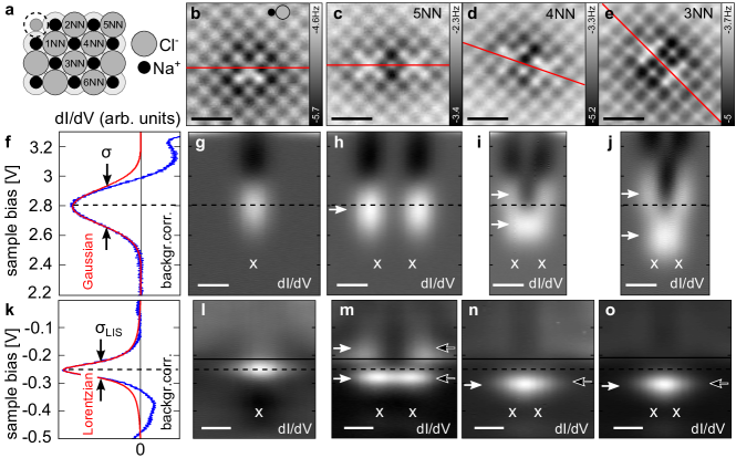
in d/d spectra. The negative ion resonance was found to have a
large Gaussian broadening (full-width half maximum (FWHM) of ) because of the strong electron–phonon coupling of the electron
in the VS to optical phonons in the NaCl bilayer. Despite this strong
coupling corresponding to an estimated Huang–Rhys parameter of about , the
associated relaxation energy of the electron in the VS is not large
enough to prohibit tunneling into unoccupied metal states and to allow
the formation of a stable occupied VS state corresponding to a
localized polaron. In contrast to the VS, the LIS was found to be
dominated by lifetime broadening with a negligible phonon broadening
in the d/d spectra, owing to the efficient screening of the
electron–phonon interaction by the metal electrons.
The atomically precise locations of intentionally created Cl
divacancies in a NaCl bilayer on Cu(111) were resolved unambiguously
using noncontact atomic force microscopy (AFM) with CO-terminated
tips (CO tips) 33, 34. Divacancies in the
nineth-nearest-neighbour (9NN), 6NN, 5NN, 4NN, 3NN and 2NN
configurations (see schematic in Fig. 1a) were
created from two Cl vacancies close to each other but not in the
vicinity of any other vacancies or defects. Constant-height AFM images
of the 5NN to 3NN divacancies and of a single vacancy are shown in
Fig. 1b-e.
The electronic structure of the VSs and the LISs of the divacancies
were characterized by constant-height d/d maps along the
line connecting the two vacancies in Fig. 1g-j and
Fig. 1l-o, respectively. All d/d data shown are
recorded using Cu-terminated tips. For the 4NN, 3NN and 2NN 111
The 2NN divacancy was less stable than the divacancies with larger
separations. divacancy configurations, two peaks with Gaussian
line shapes were observed around 2.8 V. The d/d maps show
that the state at lower energy is localized between the vacancies
(symmetric), whereas the state at higher energy has a nodal plane
between them (antisymmetric), in analogy with the bonding and
antibonding orbitals of the hydrogen molecule. Similarly, the
divacancy LISs were also observed to split into a symmetric and
an antisymmetric state. However, for small vacancy separations, the
latter state lies above the NaCl/Cu(111) interface band onset at
and overlaps with the band
continuum. Hence, only the symmetric state is observed as a
well-defined peak in d/d. The splitting of both the VSs and LISs
was found to increase with decreasing inter-vacancy distance. Tab. S1
summarizes the observed peak positions and energy splittings of the
VSs and LISs.
To study the delocalization of VSs and LISs further, short one-dimensional arrays
of vacancies, referred to in the following as vacancy chains, were
created in the 5NN (apolar NaCl direction) and the 3NN (polar NaCl
direction) configuration. They were also characterized by
constant-height CO tip AFM images (Fig. 2a,c). For
the 5NN chains, the LISs form one-dimensional quantum-well states, observed as
distinct resonances in d/d, with an increasing integer number of
nodal planes with voltage (see Fig. 2b and
Fig. S2). Surprisingly, also broad resonances are observed up to
above the interface-state band onset. These
quasi-bound LISs have a lower height in d/d, owing to the
increased lifetime broadening compared to the bound LISs.
This originates from the additional decay channel into the interface-state band. Furthermore, the
energy position of the ground-state LIS does not change significantly
from the to the chain and seems to converge to about
. The VSs in the 5NN chains only show a single
resonance peak at about because of the weak electronic
interaction between the VSs at these large intervacancy distances
(cf. Fig. 1h). In contrast, the 3NN chains displayed
in Fig. 2c have a significant interaction between the
VSs and exhibit several resonances, as shown in
Fig. 2d. The increasing number of nodal planes with
voltage shows that the VSs are delocalized over these chains despite
the strong electron–phonon coupling. In addition, the band width of
VSs increases with chain length , and is more or less saturated at
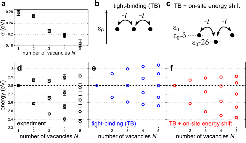
for the chain. Interestingly, the level
broadening decreases for longer chains as displayed in
Fig. 3a. This finding can be rationalized by the larger
spatial extent of the eigenstates, which decreases their relaxation
energy and accordingly the effective electron–phonon coupling.
In the following, the VS energies of the 3NN chains are compared with
the results from a simple tight-binding (TB) model. First, we assume
that each vacancy in the chain has an on-site energy
and is coupled to its next neighbour(s) with a hopping term , as
sketched in Fig. 3b. By adjusting the free fitting
parameters and to the experimental mono- and
divacancy VS energies, one can calculate the energy levels for
different chain lengths as shown in Fig. 3e. In
comparison with the experimental energy spectrum, depicted in
Fig. 3d, the level spacings for each chain could be
roughly reproduced, but the TB model does not capture the shift of the
band center towards lower energies with increasing chain length. This
shift can be explained by the electrostatic interaction between
adjacent vacancies that deepens the potential at each vacancy and
therefore lowers the on-site energy. To account for the energy
shift we introduce the parameter , which is the on-site energy shift due to a
neighbouring vacancy (see Fig. 3c). The resulting energy levels of this extended TB
model are shown in Fig. 3f. The calculated energy
spectrum now agrees very well with the experimentally observed VS levels
of the chains.
So far, the strong electron–phonon coupling, as shown by the large
broadening of the VSs, was neglected in our tight-binding models. The
role of this coupling in the formation of delocalized states by a
tunneling electron in vacancy pairs (and chains) needs to be
investigated. Here, we use a simple generalization of the
electron–phonon interaction model of the single
vacancy 30 to vacancy pairs and chains. As detailed in
the SI, the direct electronic interactions between the VSs are
described by a simple tight-binding model, and each VS is coupled
linearly to the phonon modes of the NaCl film. As we will show next, in this model,
the strong electron–phonon coupling has a profound
effect on the energy splitting and broadening of the vacancy
states. This effect is illustrated here for a divacancy using
appropriate parameters, where each single vacancy state is
coupled to a single Einstein phonon mode. Here, the electronic
interaction between the vacancies is large compared to the
phonon energy, corresponding to an electronically adiabatic
regime.
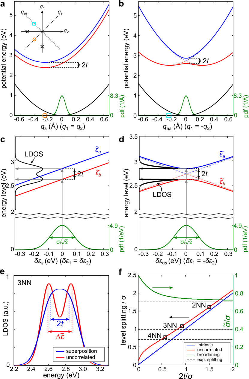
In Fig. 4a, the adiabatic potential energy surfaces
(PES) of the singly occupied, divacancy states for symmetric
displacements (where ) of the two Einstein phonon modes are
shown. They are split by , where is the direct electronic
interaction between the VSs, and both have the same shape as for the
adiabatic PES of a monovacancy. In contrast, along antisymmetric
displacements (where ) (Fig. 4b), the
corresponding PESs exhibit an avoided crossing with a minimum energy
gap of . This level repulsion will be shown to have a profound
influence on the phonon broadening and the formation of delocalized
states.
As for the single vacancy, the result for the phonon broadening of the
tunneling through the divacancy states turns out to have a simple
physical form in the prevailing strong electron–phonon coupling
limit, as detailed in the SI. The phonon broadening is determined by
probabilities for vertical Franck–Condon transitions from the
vibrational ground-state of the PES of the electronic ground-state to
vibrational states on the two PESs for the divacancy states (gray
arrows in Fig. 4c and d). In the strong
electron–phonon coupling limit, the transition probabilities are
dominated by the contribution from the linear electron–phonon
coupling terms. The corresponding phonon broadenings are then simply
obtained from the change in the divacancy energy levels
(bonding state) and
(antibonding state) with the Gaussian fluctuations of the energies
and of the vacancy 1 and 2
from their mean value due to the zero-point motions of
the phonons. As shown in the SI, this result is also valid for more
general phonon baths and electron–phonon couplings.
The strong coupling result for the phonon broadening of the divacancy
states is illustrated in Fig. 4c and d. A symmetric
fluctuation (where ) results, as shown in Fig. 4c,
in a linear dependence of and
on with slope one, but they are split by
. These Gaussian fluctuations then give rise to two overlapping
Gaussian lineshapes centered at with a variance
of
for the local density of states (LDOS).
In contrast,
the level repulsion results in a minimum energy separation
between and for an
antisymmetric fluctuation (where ). Furthermore,
breaks the symmetric and antisymmetric
character of the two coupled VSs, and they tend to localize on each
vacancy for . The resulting LDOS from
these Gaussian fluctuations, shown in Fig. 4d, consists of two relatively sharp, highly asymmetric lineshapes, with mean energies separated by more
than the energy splitting . In general, the fluctuations
and of the two vacancy
energies will be a superposition of both and
. In the case of uncorrelated energy
fluctuations
,
the LDOS is a convolution of the lineshape from
with a Gaussian lineshape with a variance
of
because and
contribute equally to
,
the variance of the single vacancy energy fluctuations.
As the Gaussian shape dominates the broadening in such a convolution,
the resulting LDOS as displayed in Fig. 4e
has a similar shape as two Gaussians with a FWHM reduced by almost
as compared to an isolated vacancy.
This decrease of
the broadening in the uncorrelated case is the underlying reason why the observed broadenings of the
levels of the chains decrease with chain size (see SI).
The two phonon modes considered here affect only one of the VSs each
and result in uncorrelated vacancy site energy fluctuations.
In reality, however, a given individual phonon mode may act on the energy of
both vacancies in a symmetric or antisymmetric fashion
(consider e.g. the motion of an ion centered between two vacancies).
Hence, partially correlated vacancy site energy fluctuations cannot be excluded.
As shown in the SI,
the two Einstein modes and their symmetric and antisymmetric fluctuations
can serve as a basis for the description of any phonon bath and
electron–phonon coupling.
Our experimental results are consistent with the assumption of fully uncorrelated fluctuations
of the two VSs.
Interestingly, in the uncorrelated case, the LDOS,
shown in Fig. 4e (red line), exhibits two peaks with an
apparent separation that is substantially larger than the intrinsic
splitting of . This result is a characteristic effect of the level
repulsion between and
and is in sharp contrast compared to a superposition of two monovacancy resonances separated by the intrinsic splitting (shown in Fig. 4e (blue line)). In the latter case, one would not be able to identify separate peaks due to the larger broadening and smaller splitting.
The enhancement of the apparent peak
separation in the uncorrelated case over the intrinsic splitting is shown
in Fig. 4f as a function of the scaled intrinsic
energy splitting , where is the broadening of
a single VS. We define the apparent peak separation
as the separation between the centers of
the two Gaussian lineshapes with broadening (FWHM)
fitted to the calculated LDOS. The
relative enhancement of the apparent
splitting is most important for small .
For large , the splitting of divacancy energy levels approaches the
intrinsic energy splitting of .
As for the single vacancy level, the broadening of a divacancy level then scales with the square root of its
relaxation energy (see SI).
The hopping terms can be extracted from Fig. 4f
by taking equal to the observed splitting
and using the single vacancy value 0.27 eV for . For example,
eV was obtained from eV
for the 3NN divacancy.
The values obtained for the hopping terms
are very reasonable as supported by density-functional theory (DFT) calculations of the unoccupied
Kohn–Sham states of Cl divacancies in NaCl(2ML)/Cu(111). As shown in
Fig. 4f, the calculated values for of the
various divacancy configurations are close to the
values for the intrinsic splittings extracted from experimental data. However,
the absolute divacancy energies are underestimated by the DFT
calculations, as expected (see Fig. S3e).
The coupling between the LISs of Cl divacancies and chains were
studied in a simple, multiple -wave scattering model of
the interface-state scattering from the positively charged vacancies
(see methods and SI). The results from this model, as indicated in
Fig. 1l-o, are able to fully capture the observed
behavior of the coupled LISs. The absence of a LIS doublet below the
onset of the interface-state band is simply understood by the
relatively strong interaction between the weakly bound LISs of the two
vacancies at small intervacancy distances. With increasing distances
between the vacancies, this interaction decreases, and a second LIS
appears below the band onset. The observed symmetric character of the
LIS below the band edge and antisymmetric character of the extended
LIS above for the 3NN vacancy are also revealed in the
calculated LDOS images (see Fig. S5). Furthermore, the obtained energies
for the LISs of the vacancy chains are in excellent agreement with the
experiments, as indicated in Fig. 2b.
In summary, from an AFM and STS study we find that the localized VSs and LISs at intentionally created Cl divacancies in a NaCl bilayer on Cu(111) form symmetric and antisymmetric states, in analogy to the bonding and antibonding orbitals of a hydrogen molecule. As expected, the energy splitting between these states increases with decreasing intervacancy distance. A comparison with theory shows that the energy splitting of the VSs is significantly enlarged by the strong coupling of the tunneling electrons with phonons in the NaCl film. Furthermore, VSs and LISs of vacancy chains form one-dimensional quantum-well states. The VS levels of the chains could be well described by a simple tight-binding model that takes the electrostatic interaction between neighbouring vacancies into account. The model provides also a microscopic understanding why the level broadening is reduced with increasing chain size. Already for about five coupled vacancies, a one-dimensional electronic band structure evolves.
Methods
Sample preparation and Cl vacancy creation.
The experiments were carried out in a home-built low-temperature combined STM and AFM operated at 5 K. A Cu(111) single-crystal sample was cleaned by several sputtering and annealing cycles. NaCl was evaporated thermally, keeping the sample temperature at about 270 K, such that defect-free, (100)-terminated NaCl bilayer islands were formed 36, 37. Bias voltages refer to the sample voltage with respect to the tip. In the spectroscopic measurements, the tunneling conductance d/d was recorded with conventional lock-in techniques with an ac bias amplitude of 25 mV at a frequency of 294 Hz. In the double-barrier tunneling junction geometry, the voltage drop across the insulating film will cause a voltage-dependent shift of the electronic levels. This tip-induced Stark shift is a few percent of the applied bias but depends only weakly on the tip distance. Therefore it is not considered here 30. The vacancies were created by bringing the Cu tip into controlled contact with the NaCl surface. Thereby a Cl atom is transfered to the tip apex, as evidenced by a characteristic contrast change in STM images and a remaining depression at the predefined Cl site. Constant-height AFM images with a CO tip 33, 34 were recorded to identify the vacancy location and exclude the generation of other close-by defects. In addition, we measured the local contact potential difference on the polar film with Kelvin probe force microscopy to ensure that the defects are indeed Cl vacancies 38.
Theoretical calculations.
Density functional calculations.
The electronic and geometric structure of the divacancies and vacancy chains in a NaCl bilayer on a Cu(111) surface were obtained using periodic density functional theory (DFT) calculations. We used the projector augmented wave (PAW) method 39, 40 as implemented in VASP 41. The exchange-correlation energy was described by the optB86b+vdW approximation42, 43. The incommensurate growth of NaCl on Cu(111) was modeled by a super cell consisting of 90 Cu atoms and 32 Na and Cl atoms in each layer (4 layers of Cu and 2 layers of NaCl), which corresponds to about 2% mismatch of NaCl distances compared to those in bulk NaCl.
Phonon broadening model.
This simple model detailed in the SI contains two key parameters: the phonon broadening (FWHM) of the single VS and the magnitude of the direct interaction energy between the two VSs. The value for is determined from the observed broadening of 0.27 eV of the single vacancy VS. The values for were adjusted to reproduce the observed energy splittings of the divacancy VSs and compared with results from the DFT calculations. For further information see the SI 44.
Interface-state band scattering model.
The coupling between the LISs of Cl divacancies are modeled with a multiple -wave scattering model of the interface-state scattering from the vacancies. This model is detailed in the SI 44. The interface-state band is modeled by a 2D free-electron band with an effective mass and a band onset . The values for and of the interface-state band were taken from STM and STS measurements37. The remaining parameter , determines the -matrix element for -wave scattering and was fitted to the observed value of -19 meV for the LIS of the vacancy.
References
- 1 Oncel, N. Atomic chains on surfaces. J. Phys.: Condens. Matter 20, 393001 (2008).
- 2 Nilius, N., Wallis, T. M. & Ho, W. Development of one-dimensional band structure in artificial gold chains. Science 297, 1853–1856 (2002).
- 3 Loth, S., Baumann, S., Lutz, C. P., Eigler, D. M. & Heinrich, A. J. Bistability in atomic-scale antiferromagnets. Science 335, 196–199 (2012).
- 4 Blumenstein, C. et al. Atomically controlled quantum chains hosting a Tomonaga-Luttinger liquid. Nature Phys. 7, 776–780 (2011).
- 5 Nadj-Perge, S. et al. Observation of Majorana fermions in ferromagnetic atomic chains on a superconductor. Science 346, 602–607 (2014).
- 6 Crain, J. N. & Pierce, D. T. End states in one-dimensional atom chains. Science 307, 703–706 (2005).
- 7 Barke, I. et al. Low-dimensional electron gas at semiconductor surfaces. Solid State Commun. 142, 617–626 (2007).
- 8 Fölsch, S., Yang, J., Nacci, C. & Kanisawa, K. Atom-by-atom quantum state control in adatom chains on a semiconductor. Phys. Rev. Lett. 103, 096104 (2009).
- 9 Wang, S., Wang, W. & Lin, N. Resolving band-structure evolution and defect-induced states of single conjugated oligomers by scanning tunneling microscopy and tight-binding calculations. Phys. Rev. Lett. 106, 206803 (2011).
- 10 Riss, A. et al. Local electronic and chemical structure of oligo-acetylene derivatives formed through radical cyclizations at a surface. Nano Lett. 14, 2251–2255 (2014).
- 11 Repp, J., Liljeroth, P. & Meyer, G. Coherent electron-nuclear coupling in oligothiophene molecular wires. Nature Phys. 6, 975–979 (2010).
- 12 Olsson, F. et al. Localization of the Cu(111) surface state by single Cu adatoms. Phys. Rev. Lett. 93, 206803 (2004).
- 13 Fölsch, S., Martínez-Blanco, J., Yang, J., Kanisawa, K. & Erwin, S. C. Quantum dots with single-atom precision. Nat. Nanotechnol. 9, 505–508 (2014).
- 14 Koenraad, P. M. & Flatté, M. E. Single dopants in semiconductors. Nature Mat. 10, 91–100 (2011).
- 15 Schofield, S. et al. Quantum engineering at the silicon surface using dangling bonds. Nature Commun. 4, 1649 (2013).
- 16 Lorke, A., Kotthaus, J. & Ploog, K. Coupling of quantum dots on GaAs. Phys. Rev. Lett. 64, 2559–2562 (1990).
- 17 Hameau, S. et al. Strong electron-phonon coupling regime in quantum dots: Evidence for everlasting resonant polarons. Phys. Rev. Lett. 83, 4152–4155 (1999).
- 18 Haider, M. B. et al. Controlled coupling and occupation of silicon atomic quantum dots at room temperature. Phys. Rev. Lett. 102, 046805 (2009).
- 19 Sun, Z., Swart, I., Delerue, C., Vanmaekelbergh, D. & Liljeroth, P. Orbital and charge-resolved polaron states in CdSe dots and rods probed by scanning tunneling spectroscopy. Phys. Rev. Lett. 102, 196401 (2009).
- 20 Leturcq, R. et al. Franck–Condon blockade in suspended carbon nanotube quantum dots. Nature Phys. 5, 327–331 (2009).
- 21 Seufert, K. et al. Controlled interaction of surface quantum-well electronic states. Nano Lett. 13, 6130–6135 (2013).
- 22 Andresen, S. E. et al. Charge state control and relaxation in an atomically doped silicon device. Nano Lett. 7, 2000–2003 (2007).
- 23 Mujica-Martinez, C. A., Nalbach, P. & Thorwart, M. Organic -conjugated copolymers as molecular charge qubits. Phys. Rev. Lett. 111, 016802 (2013).
- 24 Lent, C. S., Tougaw, P. D., Porod, W. & Bernstein, G. H. Quantum cellular automata. Nanotechnology 4, 49 (1993).
- 25 Nilius, N., Wallis, T. & Ho, W. Influence of a heterogeneous Al2O3 surface on the electronic properties of single Pd atoms. Phys. Rev. Lett. 90, 046808 (2003).
- 26 Repp, J., Meyer, G., Stojković, S., Gourdon, A. & Joachim, C. Molecules on insulating films: Scanning-tunneling microscopy imaging of individual molecular orbitals. Phys. Rev. Lett. 94, 026803 (2005).
- 27 Nilius, N., Wallis, T., Persson, M. & Ho, W. Distance dependence of the interaction between single atoms: Gold dimers on NiAl(110). Phys. Rev. Lett. 90, 196103 (2003).
- 28 Sonnleitner, T., Swart, I., Pavliček, N., Pöllmann, A. & Repp, J. Molecular symmetry governs surface diffusion. Phys. Rev. Lett. 107, 186103 (2011).
- 29 Kawai, S. et al. Atom manipulation on an insulating surface at room temperature. Nature Commun. 5, 4403 (2014).
- 30 Repp, J., Meyer, G., Paavilainen, S., Olsson, F. & Persson, M. Scanning tunneling spectroscopy of Cl vacancies in NaCl films: Strong electron-phonon coupling in double-barrier tunneling junctions. Phys. Rev. Lett. 95, 225503 (2005).
- 31 Zielasek, V., Hildebrandt, T. & Henzler, M. Surface color centers on epitaxial NaCl films. Phys. Rev. B 62, 2912–2919 (2000).
- 32 Simon, B. The bound state of weakly coupled Schrödinger operators in one and two dimensions. Ann. Phys. 97, 279–288 (1976).
- 33 Gross, L., Mohn, F., Moll, N., Liljeroth, P. & Meyer, G. The chemical structure of a molecule resolved by atomic force microscopy. Science 325, 1110–1114 (2009).
- 34 Mohn, F., Schuler, B., Gross, L. & Meyer, G. Different tips for high-resolution atomic force microscopy and scanning tunneling microscopy of single molecules. Appl. Phys. Lett. 102, 073109 (2013).
- 35 The 2NN divacancy was less stable than the divacancies with larger separations.
- 36 Bennewitz, R. et al. Ultrathin films of NaCl on Cu(111): A LEED and dynamic force microscopy study. Surf. Sci. 438, 289–296 (1999).
- 37 Repp, J., Meyer, G. & Rieder, K.-H. Snell’s law for surface electrons: Refraction of an electron gas imaged in real space. Phys. Rev. Lett. 92, 036803 (2004).
- 38 Gross, L. et al. Investigating atomic contrast in atomic force microscopy and Kelvin probe force microscopy on ionic systems using functionalized tips. Phys. Rev. B 90, 155455 (2014).
- 39 Kresse, G. & Joubert, D. From ultrasoft pseudopotentials to the projector augmented-wave method. Phys. Rev. B 59, 1758–1775 (1999).
- 40 Blöchl, P. E. Projector augmented-wave method. Phys. Rev. B 50, 17953–17979 (1994).
- 41 Kresse, G. & Furthmüller, J. Efficient iterative schemes for ab initio total-energy calculations using a plane-wave basis set. Phys. Rev. B 54, 11169–11186 (1996).
- 42 Thonhauser, T. et al. Van der waals density functional: Self-consistent potential and the nature of the van der waals bond. Phys. Rev. B 76, 125112 (2007).
- 43 Klimeš, J. c. v., Bowler, D. R. & Michaelides, A. Van der Waals density functionals applied to solids. Phys. Rev. B 83, 195131 (2011).
- 44 See Supporting Information at http://.
- 45 Lyo, I.-W. & Avouris, P. Negative differential resistance on the atomic scale: Implications for atomic scale devices. Science 245, 1369–1371 (1989).
- 46 At positive voltages, the NDC arises from the increase of the tunnel barrier for resonant tunneling through the VS with voltages greater than the VS 26; for negative voltages the NDC stems from a nonuniform tip density of states 45.
Acknowledgments
We thank R. Allenspach for comments and acknowledge financial support
from the ERC Advanced Grant CEMAS (agreement no. 291194) and the EU projects PAMS (610446) and
QTea (317485). Allocation of computer resources through SNAC and CSC is gratefully
acknowledged.
Author contributions
All authors contributed to the preparation of the paper. B.S., N.P., L.G, G.M. and J.R. conducted the experiments. M.P. and S.P. developed the coupling models and performed the DFT calculations.
Additional information
Correspondence and requests for materials should be addressed to B.S. (e-mail: bsc@zurich.ibm.com).