Layered Topological Crystalline Insulators
Abstract
Topological crystalline insulators (TCIs) are insulating materials whose topological property relies on generic crystalline symmetries. Based on first-principles calculations, we study a three-dimensional (3D) crystal constructed by stacking two-dimensional TCI layers. Depending on the inter-layer interaction, the layered crystal can realize diverse 3D topological phases characterized by two mirror Chern numbers (MCNs) () defined on inequivalent mirror-invariant planes in the Brillouin zone. As an example, we demonstrate that new TCI phases can be realized in layered materials such as a PbSe (001) monolayer/h-BN heterostructure and can be tuned by mechanical strain. Our results shed light on the role of the MCNs on inequivalent mirror-symmetric planes in reciprocal space and open new possibilities for finding new topological materials.
New topological states of matter, topological crystalline insulators Fu (2011), have been identified that extend the topological classification beyond the prototypical classification based on time reversal symmetry Hasan and Kane (2010); Qi and Zhang (2011). In TCIs, topological properties of electronic structure such as the presence of robust metallic surface states arise from crystal symmetries instead of time-reversal symmetries. There are many proposed TCI phases depending on different crystal symmetries Fang et al. (2012); Slager et al. (2013); Chiu et al. (2013); Fang et al. (2013); Alexandradinata et al. (2014); Shiozaki and Sato (2014), yet those relying on mirror symmetry Hsieh et al. (2012) are of particular interest as they have been experimentally observed in, for example, IV-VI semiconductors SnTe, , and Dziawa et al. (2012); Liang et al. (2013); Tanaka et al. (2013); Okada et al. (2013); Xu et al. (2012). More materials are theoretically proposed to realize the TCI phases such as rocksalt semiconductors Sun et al. (2013); Tang et al. (2014), pyrochlore iridates Kargarian and Fiete (2013), graphene systems Kindermann (2013), heavy fermion compounds Weng et al. (2014); Ye et al. (2013), and antiperovskites Hsieh et al. (2014), including two-dimensional (2D) materials such as SnTe thin films Liu et al. (2014); Ozawa et al. (2014) and a (001) monolayer of PbSe Wrasse and Schmidt (2014).
Mirror-symmetric TCIs are mathematically characterized by mirror Chern numbers. The MCN is a topological invariant defined by where and are Chern numbers of Bloch states with the opposite eigenvalues of a mirror operator () calculated on the mirror-invariant plane at in the Brillouin zone (BZ). In a three-dimensional (3D) crystal, there is a second MCN () defined on the mirror-invariant plane at the boundary of the BZ (in units of , where is the length of the primitive lattice vector along the -axis) Teo et al. (2008). Moreover, considering different mirror symmetries, multiple pairs of MCNs () can be simultaneously present in three dimensions. A complete characterization of 3D TCIs requires consideration of all the MCNs, which may allow for the possibility of new states of matter, where MCNs are locked together or undergo separate transitions. Nonetheless, previous study based only on has not explored this situation.
In this paper, by considering MCNs on all inequivalent mirror-symmetric planes in reciprocal space, we study new topological states of matter realized in a 3D layered crystal generated by stacking 2D TCI layers. We show that the layered system realizes a new class of 3D TCIs when inter-layer interaction is weak, which we will refer to as a layered TCI. The layered TCI is characterized by equal and nonzero first and second MCNs with a number of metallic surface states eqaul to . Increasing the inter-layer interaction, we then show that the layered TCI undergoes topological phase transitions that change the MCNs . Based on first-principles calculations, we predict that a heterostructure consisting of alternating layers of PbSe monolayer and hexagonal BN (h-BN) sheet realizes the layered TCI indexed by (2,2), and that it undergoes distinct topological phase transitions in the sequence (): under external uniaxial tensile strain. Our findings shed light on new states of matter allowed by the presence of multiple MCNs in a 3D crystal. They may also help guide the discovery of more topological materials.
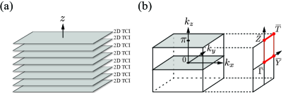
Before presenting the results, we first briefly explain how 2D TCI layers with a non-zero MCN () can be stacked into a new class of 3D TCIs characterized by . Consider first a layered system consisting of 2D TCIs with stacked along the normal direction to the plane (defined as -direction) as shown in FIG. 1(a). The layered system then respects the mirror symmetry that defines the MCN of the 2D TCI in the plane of each layer. Now, let us initially assume that the interaction between the layers is negligibly weak, so that every cross section of the 3D BZ at constant is essentially a copy of the 2D BZ of the film. In particular, the mirror invariant planes at and [See Fig. 1(b)] should adopt the same MCN as the 2D TCI, and thus be indexed by . For mirror symmetries inequivalent to (if any), the corresponding MCNs are all trivial (0,0) because the mirror planes allowed by the layered geometry are normal to the films, and the crystalline surfaces respecting the mirror symmetries are essentially the 2D TCIs without metallic (surface) states. This means that the proposed TCI are characterized by the coupled MCNs () for and () for any mirror symmetry inequivalent to . Turning on the inter-layer interaction in a way that respects the mirror symmetry, the MCNs should persist within a finite range of the interaction, until the system experiences a topological phase transition through a gap closure Smith et al. (2011), which can lead either to a new topological state where the indices are decoupled or to a conventional insulating state.
We demonstrate the topological phases associated with MCNs and their transitions from first principles by applying the above theory to a PbSe/h-BN heterostructure. Our calculation is performed with density functional theory (DFT) including the Perdew-Burke-Ernzerhof Perdew et al. (1996) generalized gradient approximation as implemented in the QUANTUM ESPRESSO package Giannozzi et al. (2009). The atomic potentials are modeled by norm-conserving, optimized, designed nonlocal pseudopotentials with fully relativistic spin-orbit interaction generated by the OPIUM package Rappe et al. (1990); Ramer and Rappe (1999). The wave functions are expanded in a plane-wave basis with an energy cutoff of 650 eV. For computational convenience, the energy cutoff is reduced to 540 eV when calculating the surface band structure of PbSe(001) monolayers. The van der Waals interaction is described based on the semiempirical dispersion-correction DFT (DFT-D) method Grimme (2006). The tight-binding model, introduced in Ref. Hsieh et al. (2012), is also employed to analyze the DFT results on (001) PbSe layers using parameter sets obtained from our DFT calculations. The results are consistent with the previous studies of IV-VI semiconductors, including PbSe Hsieh et al. (2012); Liu et al. (2014); Wrasse and Schmidt (2014). The unit cell of the PbSe/h-BN heterostructure is generated by contracting the in-plane lattice constants of the h-BN sheet so that they match the pristine lattice constant of the PbSe. We have checked that the artificial contraction has negligible influence on the electronic structure near the Fermi energy, as h-BN has a wide band gap.
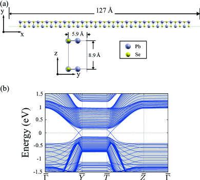
We first build a layered TCI based on (001) PbSe monolayers. Whereas PbSe is a trivial insulator in a 3D rocksalt geometry, (001) PbSe monolayer is expected to be a 2D TCI, indexed by the MCN Wrasse and Schmidt (2014). As shown in Fig. 2(a), we consider a system consisting of PbSe monolayers stacked along the perpendicular direction to the plane ([001]-direction), so that Pb (and Se) atoms form chains along [001], separated by 8.9 Å. The other crystal parameters are set to those of the bulk PbSe. In this way, the inter-layer interaction remains weak, and the resulting system is a layered TCI indexed by associated with the (001) mirror plane. The system respects additional mirror symmetries about {100} and {110} mirror planes, on which the MCNs are all trivial as discussed above.
The calculated MCNs signal the presence of four surface states on the mirror-symmetric facets. As depicted in Fig. 1(b), for a surface containing , the surface BZ has two inequivalent mirror-symmetric lines, - - and - - which are the projections of the and mirror-planes into the surface plane. The absolute values of the MCNs and dictate the numbers of pairs of counter-propagating surface states on the and mirror lines, respectively. It follows that there must exist two pairs of surface states along each line. To look for the surface states guaranteed by the MCNs, we calculate the 2D band structure for the slab geometry illustrated in Fig. 2(a). Figure 2(b) shows the band structure for a slab exposing the (100) surface to vacuum along high symmetric lines [See Fig. 1(b)]. As expected, in addition to the bulk states in the gray region, we find surface states that traverse the gap forming Dirac points on the mirror-symmetric lines - and - . It is clear from the results that the (100) surface has four total Dirac points [two shown in Fig. 2(b) and two more at the minus of these], dictated by their sum of the absolute value . Note that - and - host no metallic surface states. This proves on (010) mirror planes.
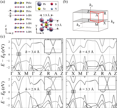
Having demonstrated the layered TCI with in the layered PbSe system, we now consider a more realistic material. Above, we manually fixed the distance between the PbSe monolayers to 8.9 Å to make the inter-layer interaction weak, but this is energetically unfavorable as the PbSe layers feel a repulsive force as the same cations and anions in different layers face each other at the interface. To stabilize the system, while keeping the inter-layer interaction weak, we insert a h-BN sheet which serves as spacer between the neighboring PbSe layers, as shown in Fig. 3(a). A h-BN sheet is a normal insulator with a wide band gap of 5 eV, which suggests that the band topology of the heterostructure should be governed by bands from the PbSe films. We find that the heterostructure has an equilibrium distance () of 3.4 Å, with a binding energy of 0.08 eV per unit cell of PbSe, which indicates that the interaction is in the typical van der Waals regime.
In Fig. 3, we show the band structures of the PbSe/h-BN heterostructure along the high-symmetric lines in the BZ calculated for various PbSe-h-BN inter-layer distances (). First, at equilibrium , the system is found to be semi-metallic with a small hole pocket at on the plane and an electron pocket near on the plane. Then, by increasing the inter-layer distance from (), the band gap at keeps increasing, and the system eventually becomes an insulator when Å. Increasing further, we find that the system remains insulating without closing the band gap. Thus, we assign the layered TCI phase indexed by (2,2) to the system when .
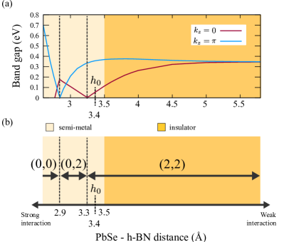
Conversely, by decreasing the inter-layer distance from equilibrium , which enhances the inter-layer interaction, we find that the system undergoes topological phase transitions signaled by the appearance of the Dirac points. As presented in Fig. 3(c), the Dirac points appear at Å and Å on the and mirror planes, respectively. The MCNs, calculated using all the valence bands on each mirror-symmetric plane, change from (2,2) to (0,2) and from (0,2) to (0,0) as passes through 3.24 Å and Å, respectively. All the topological phase transitions occur in a a region where the system is a semimetal because of overlapping bands. Below Å, the valence band maximum becomes higher in energy than the conduction band minimum on the plane, so the MCN is not defined. Therefore, from the strong to weak inter-layer interaction regimes, four distinct topological phases appear, as shown in the phase diagram in Fig. 4(b); a trivial semimetal phase with (0,0), a topological semimetal phase with , a topological semimetal phase with , and the layered TCI phase with . Although the heterostructure of PbSe/h-BN sheets is expected to be semi-metallic at ambient pressure, we expect that these phases should be accessible under mechanical strain including the proposed (2,2) layered TCI or by inserting another h-BN sheet between PbSe layers. We also expect that the phase transitions demonstrated in this system should be representative of layered TCIs, and heterostructures of 2D TCIs can be considered as hosts of diverse topological phases accessible by engineering the inter-layer interaction. The calculated inter-layer distances may vary depending on details of the crystal geometry like a stacking registry between PbSe-h-BN layers, yet the qualitative features should remain intact.
Finally, we note that layered TCIs are analogous to weak topological insulators Fu et al. (2007); Mong et al. (2012). Weak TIs, characterized by zero invariant yet non-zero weak topological indices , is essentially a stack of 2D TI layers along the perpendicular direction that corresponds to in the BZ Fu et al. (2007), having even numbers of robust Dirac cones at the surfaces perpendicular to the 2D TI layers Ringel et al. (2012); Mong et al. (2012). Similarly, 3D TCI with the same first and second mirror Chern numbers is like layered 2D TCIs, having Dirac cones on the surfaces normal to the 2D TCI layers. Also, like weak topological indices, () are sensitive to the translational symmetry of the crystal. For instance, we find that a period-doubling along the -axis changes the MCNs : , and due to the BZ folding, which can be induced by inter-layer bonding or a registry shift between 2D TCI layers. Indeed, we have found the MCNs to be (4,0) when stacking the PbSe layers with a registry shift atoms between Pb and Se atoms in every layer. Notwithstanding the sensitivity, it is important to note that the total number of surface Dirac cones on the mirror symmetric surfaces, dictated by , is invariant under the period-doubling, and the second MCN is thus indispensable for characterizing the layered TCIs, and indeed all 3D TCIs.
In conclusion, we propose new topological states of matter generated by stacking 2D TCIs, where simultaneous consideration of multiple MCNs is necessary. In the non-interacting limit between layers, the layered TCI phase emerges where the first and second MCNs () are coupled. The layered TCI is a generic class of 3D TCIs which can apply to a range of 2D TCI materials. For example, a SnTe thin film, which is expected to be a 2D TCI when cleaved into an odd number of (001) layers Liu et al. (2014), can play the role of the PbSe layer in the PbSe/h-BN heterostructure, thus realizing the layered TCI indexed by (2,2) when the layers are well separated. Apart from the non-interacting regime, we find topological semimetal phases indexed by and and trivial semimetal phase with . Despite the presence of metallic bulk states, the phase transitions should be observable via experimental techniques such as angle-resolved photoemission spectroscopy. Our findings shed light on the possibility of new TCI phases relying on the fact that a crystal in three dimensions can have multiple MCNs hosted on inequivalent mirror planes in reciprocal lattice. These may open the way towards the search for new topological materials, based on which quantum devices for electronics as well as spintronics can be built.
Acknowledgements.
We thank Fan Zhang and Steve M. Young for helpful discussion. CLK acknowledges support as a Simons Investigator grant from the Simons Foundation. EJM acknowledges support from the Department of Energy under Grant No. FG02-ER45118. AMR acknowledges support from the Department of Energy Office of Basic Energy Sciences, under grant number DE-FG02-07ER15920. Computational support is provided by the HPCMO of the U.S. DOD and the NERSC of the U.S. DOE.References
- Fu (2011) L. Fu, Phys. Rev. Lett. 106, 106802 (2011).
- Hasan and Kane (2010) M. Z. Hasan and C. L. Kane, Rev. Mod. Phys. 82, 3045 (2010).
- Qi and Zhang (2011) X.-L. Qi and S.-C. Zhang, Rev. Mod. Phys. 83, 1057 (2011).
- Fang et al. (2012) C. Fang, M. J. Gilbert, and B. A. Bernevig, Phys. Rev. B 86, 115112 (2012).
- Slager et al. (2013) R.-J. Slager, A. Mesaros, V. Juricic, and J. Zaanen, Nature Physics 9, 98 (2013).
- Chiu et al. (2013) C.-K. Chiu, H. Yao, and S. Ryu, Phys. Rev. B 88, 075142 (2013).
- Fang et al. (2013) C. Fang, M. J. Gilbert, and B. A. Bernevig, Phys. Rev. B 87, 035119 (2013).
- Alexandradinata et al. (2014) A. Alexandradinata, C. Fang, M. J. Gilbert, and B. A. Bernevig, Phys. Rev. Lett. 113, 116403 (2014).
- Shiozaki and Sato (2014) K. Shiozaki and M. Sato, Phys. Rev. B 90, 165114 (2014).
- Hsieh et al. (2012) T. H. Hsieh, H. Lin, J. Liu, W. Duan, A. Bansil, and L. Fu, Nat. Commun. 3, 982 (2012).
- Dziawa et al. (2012) P. Dziawa, B. J. Kowalski, K. Dybko, R. Buczko, A. Szczerbakow, M. Szot, E. Łusakowska, T. Balasubramanian, B. M. Wojek, M. H. Berntsen, O. Tjernberg, and T. Story, Nature Materials 11, 1023 (2012).
- Liang et al. (2013) T. Liang, Q. Gibson, J. Xiong, M. Hirschberger, S. P. Koduvayur, R. J. Cava, and N. P. Ong, Nat. Commun. 4, 2696 (2013).
- Tanaka et al. (2013) Y. Tanaka, T. Shoman, K. Nakayama, S. Souma, T. Sato, T. Takahashi, M. Novak, K. Segawa, and Y. Ando, Phys. Rev. B 88, 235126 (2013).
- Okada et al. (2013) Y. Okada, M. Serbyn, H. Lin, D. Walkup, W. Zhou, C. Dhital, M. Neupane, S. Xu, Y. J. Wang, R. Sankar, F. Chou, A. Bansil, M. Z. Hasan, S. D. Wilson, L. Fu, and V. Madhavan, Science 341, 1496 (2013).
- Xu et al. (2012) S.-Y. Xu, C. Liu, N. Alidoust, M. Neupane, D. Qian, I. Belopolski, J. D. Denlinger, Y. J. Wang, H. Lin, L. A. Wray, G. Landolt, B. Slomski, J. H. Dil, A. Marcinkova, E. Morosan, Q. Gibson, R. Sankar, F. C. Chou, R. J. Cava, A. Bansil, and M. Z. Hasan, Nat. Commun. 3, 1192 (2012).
- Sun et al. (2013) Y. Sun, Z. Zhong, T. Shirakawa, C. Franchini, D. Li, Y. Li, S. Yunoki, and X.-Q. Chen, Phys. Rev. B 88, 235122 (2013).
- Tang et al. (2014) P. Tang, B. Yan, W. Cao, S.-C. Wu, C. Felser, and W. Duan, Phys. Rev. B 89, 041409 (2014).
- Kargarian and Fiete (2013) M. Kargarian and G. A. Fiete, Phys. Rev. Lett. 110, 156403 (2013).
- Kindermann (2013) M. Kindermann, (2013), arXiv:1309.1667 .
- Weng et al. (2014) H. Weng, J. Zhao, Z. Wang, Z. Fang, and X. Dai, Phys. Rev. Lett. 112, 016403 (2014).
- Ye et al. (2013) M. Ye, J. W. Allen, and K. Sun, (2013), arXiv:1307.7191 .
- Hsieh et al. (2014) T. H. Hsieh, J. Liu, and L. Fu, Phys. Rev. B 90, 081112 (2014).
- Liu et al. (2014) J. Liu, T. H. Hsieh, P. Wei, W. Duan, J. Moodera, and L. Fu, Nature Materials 13, 178 (2014).
- Ozawa et al. (2014) H. Ozawa, A. Yamakage, M. Sato, and Y. Tanaka, Phys. Rev. B 90, 045309 (2014).
- Wrasse and Schmidt (2014) E. O. Wrasse and T. M. Schmidt, Nano Lett. 14, 5717 (2014).
- Teo et al. (2008) J. C. Y. Teo, L. Fu, and C. L. Kane, Phys. Rev. B 78, 045426 (2008).
- Smith et al. (2011) J. C. Smith, S. Banerjee, V. Pardo, and W. E. Pickett, Phys. Rev. Lett. 106, 056401 (2011).
- Perdew et al. (1996) J. P. Perdew, K. Burke, and M. Ernzerhof, Phys. Rev. Lett. 77, 3865 (1996).
- Giannozzi et al. (2009) P. Giannozzi, S. Baroni, N. Bonini, M. Calandra, R. Car, C. Cavazzoni, D. Ceresoli, G. L. Chiarotti, M. Cococcioni, I. Dabo, A. D. Corso, S. de Gironcoli, S. Fabris, G. Fratesi, R. Gebauer, U. Gerstmann, C. Gougoussis, A. Kokalj, M. Lazzeri, L. Martin-Samos, N. Marzari, F. Mauri, R. Mazzarello, S. Paolini, A. Pasquarello, L. Paulatto, C. Sbraccia, S. Scandolo, G. Sclauzero, A. P. Seitsonen, A. Smogunov, P. Umari, and R. M. Wentzcovitch, J. Phys.: Condens. Matter. 21, 395502 (2009).
- Rappe et al. (1990) A. M. Rappe, K. M. Rabe, E. Kaxiras, and J. D. Joannopoulos, Phys. Rev. B 41, 1227 (1990).
- Ramer and Rappe (1999) N. J. Ramer and A. M. Rappe, Phys. Rev. B 59, 12471 (1999).
- Grimme (2006) S. Grimme, J. Comput. Chem. 27, 1787 (2006).
- Fu et al. (2007) L. Fu, C. L. Kane, and E. J. Mele, Phys. Rev. Lett. 98, 106803 (2007).
- Mong et al. (2012) R. S. K. Mong, J. H. Bardarson, and J. E. Moore, Phys. Rev. Lett. 108, 076804 (2012).
- Ringel et al. (2012) Z. Ringel, Y. E. Kraus, and A. Stern, Phys. Rev. B 86, 045102 (2012).