Geometrically Enhanced Quantum Oscillatory Signal and Nonzero Berry’s Phase in Indium Arsenide Surface
Abstract
In a system accommodating both surface and bulk conduction channels, a long-standing challenge is to extract weak Shubnikov-de Haas oscillation signal in the surface from a large background stemming from the bulk. Conventional methods to suppress the bulk conduction often involve doping, an intrusive approach, to reduce the bulk carrier density. Here we propose a geometric method, i.e. attaching a metal shunt to the indium arsenide epilayer, to redistribute current and thus enhance the oscillation-to-background ratio. This allows us, for the first time, to observe clear quantum oscillations and nonzero Berry’s phase at the surface of indium arsenide. We also identify the existence of a Rashba type spin-orbit interaction, on the InAs surface, with a large coupling constant . We anticipate wide applicability of this non-intrusive architecture in similar systems such as topological insulators.
pacs:
73.61.Ey, 72.20.-i, 72.80.Ey, 73.50.JtIndium arsenide (InAs), an ordinary narrow-gap semiconductor with high intrinsic mobility and considerable field effect, is a promising material in electronic applications ko-nature-2010 . Yet a surface state, with a sheet density of residing on the free surfaces of InAs as due to band bending, has been known for decades olsson-prl-1996 . The recent rise of topological insulators (TIs) has enriched the pool of host materials with surface state Kane-TI . Dimensionality and energy dispersion of these TI surface states are frequently studied using transport measurements such as the Shubnikov-de Haas (SdH) oscillation shoenberg-book . Meanwhile, the quantum oscillations from the free surfaces intrinsic to InAs was seldom reported. The regular Hall-bar-type geometry measures the sample as a homogeneous system and thus provides an averaged signal. The intimate contact between the surface state and underlying bulk, however, impedes the extraction of weak SdH signal of the former from a large resistance background of the latter. In TIs, for example, it is a challenging task to suppress the bulk carrier density to enhance the surface dominated transport analytis-natphys-2010 .
In this letter, we propose a novel architecture to remove this long-standing obstacle. We use a metal-shunted Hall bar to enhance the SdH signal in the InAs surface. The enhancement achieved here is often called “geometric ”, i.e. modifying a conductor by changing its geometric shape, which has been defined for the enhanced magnetoresistance in semiconductors Allgaier-JAP ; solin-science . We apply this architecture on InAs to extract efficiently the SdH signals in the surface state. From the SdH Oscillations, we further discover a nonzero Berry’s phase as a manifestation of the Rashba coupling driven by the inversion asymmetry.

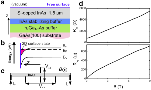
The experimental sample is a m thick Si-doped InAs epilayer on GaAs substrate (Fig. 1a, also see Methods). The metamorphic buffer layer technique is employed to absorb strain from lattice mismatch and prevent vertical propagation of dislocations to maintain the quality of the top InAs active layers meta_Lub . It also aligns the energy bands between GaAs and InAs, avoiding possible formation of two-dimensional electron systems across the heterojunction. We are confident to argue that any signals of 2D nature shall originate from the InAs surface state (see Fig. 1b).
As a control experiment, we first show the transport measurements in a regular InAs Hall bar without a metal shunt, as sketched in Fig. 1c. The longitudinal magnetoresistance and Hall resistance at perpendicular magnetic fields are shown in Fig. 1d. Two curves are smooth, as the large background signals wash out the quantum oscillations. The nonlinearity in at low field implies the existence of a parallel conducting channel, i.e. the surface state Wieder-APL-1974 ; xiong-prb-2012 .

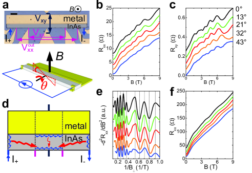
The shunted Hall bar, shown in Fig. 2a, is prepared via conventional lithography procedures (see Methods). At 10 K, the and measured in the shunted bar are shown in Fig. 2b and c, respectively. In contrast to the smooth curves observed in the regular Hall bar, both and exhibit pronounced oscillation superimposed on a suppressed background (see the values on the vertical axis), or, an enhanced oscillation-to-background ratio has been achieved.
To uncover the origin of the oscillations, we scan the angular dependence of the SdH oscillations by rotating the sample in a magnetic field to different angles (Fig. 2a). In Figs. 2b and c, local minima (maxima) show a systematic shift against , whereas in Fig. 2e, they are aligned against at all angles. This clearly exhibits the 2D nature qu-science-2010 ; analytis-natphys-2010 of the surface state in InAs.
Intriguing yet simple mechanisms are driving the enhancement. The metal shunt redistributes the current injected into the InAs bar as electrons favour the paths of the lowest resistance, according to the Ohm’s law. Finite element simulations reveal an inhomogeneous current distribution in the InAs bar. Most electrons flow into(out of) the metal shunt along the -direction near two current leads; while a small portion of them traverses the InAs bar without entering the shunt. The middle part of the InAs bar, i.e. between two electrodes, is effectively shorted by the metal. The background signal measured locally at is thus much suppressed, again, according to Ohm’s law.
The local current reduction seems to suggest a weakened oscillatory signal too. The SdH oscillations in the surface layer, however, originate from the scattering between edge states localized at InAs bar boundaries buttiker-prb-1988 ; vanwees-prb-1989 , demanding a global picture on the entire conductor (Fig. 2d). In our geometry, as a current is injected under a perpendicular magnetic field, abundant edge states are formed close to the left and right edges of the InAs bar. In the 2D surface, the scattering events also happen between edge states at the left (right) and lower edges. Therefore, the SdH signal probed at the contacts is an average over contributions from three edges (Fig. 2d). The reduction of the SdH signal is hence less significant than the suppression in the background. And the oscillation-to-background signal ratio is enhanced. This mechanism relies on the geometry manipulation creating current inhomogeneity, not on the intrusive modification of material properties, and is thus achievable with less technological complication.
We emphasise that the enhancement, as a geometric effect, is highly sensitive to the electrode locations where the signal is probed. In Fig. 2f, we plot the oscillations in measured with an additional set of outer electrodes V (see Figs. 2a), where the current density is higher. We observe a sharp contrast to the signal acquired at inner contacts: At outer contacts, the SdH oscillations are buried by a larger background magnetoresistance (compare to that measured at inner contacts), and are thus less distinguishable.
The data allows us to extract the effective mass in the surface state by fitting the temperature dependence of the oscillatory component into the Lifshits-Kosevich formula. This yields which is close to obtained by using low-temperature scanning tunneling microscopy canali-InAs-surface-1998 .

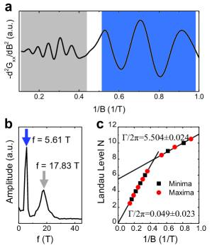
The frequency of the SdH oscillations also contains the information of carrier density and Berry phase in the surface state. However, we notice that, in the high field regime, the phase difference between and is approximately , instead of . Such discrepancy is attributed to the coexistence of both surface and bulk conducting channels. The conductance, not resistance, bears the correct information to analyse the carrier density and Berry phase xiong-prb-2012 ; Shrestha-prb-2014 . Following a standard procedurexiong-prb-2012 ; Shrestha-prb-2014 , we convert the resistance to conductance and extract oscillatory extrema from the negative second derivative (Fig. 3a). The Fourier analysis reveals a single frequency T for the signal below T (called low field regime thereafter, Fig.3b). This corresponds to a sheet density cm-2, according to the Onsager relation , and a Fermi wave vector cm-1 since . Here, is Planck constant divided by and is the absolute value of the elementary charge. At fields higher than T (called high field regime thereafter), a frequency T is obtained, suggesting a sheet density cm-2 for a spin-filtered surface state.
The presence of two dominant frequencies in the SdH signal strongly indicates the existence of two Fermi circles in the 2D surface state. All experimental features are consistent with a 2D Bychkov-Rashba model comprising a parabolic energy dispersion and a Rashba spin-orbit coupling . Here is the Rashba coupling constant, a 2D wave-vector, and the Pauli matrix. To estimate , we employ the Onsager formula to relate the higher frequency and the lower one to the Fermi wave vectors that are determined by the two polarization branches originating from the Rashba splitting, i.e. . As the Fermi energy can be estimated using the total carrier density , we obtain in the leading order of ,
| (1) |
The Fermi energy is assumed to be larger than the Rashba energy . The total sheet carrier density is and the frequencies are and . Using Eq. 1, we find a large Rashba constant . This value is comparable to the ones in surface alloys ast-surface-alloy-prl-2007 but still about one order of magnitude larger than those in typical semiconductor heterojunctions nitta-rashba-2deg-prl-1997 . The corresponding Rashba energy is also in par with the surface states in Au lashell-au-surface-prl-1996 or Bi koroteev-bi-prl-2004 , and quantum wells states formed on Pb thin film dil-pb-fim-prl-2008 . The Fermi surface is about 8.54 meV from the bottom of the inner Rashba band (the band touching point), and 27.15 meV from the bottom of the outer band.
We may also obtain, from the SdH signal, the phase shift encoded in the oscillating part of the longitudinal magneto-conductance
| (2) |
In solid systems, and the Berry’s phase berry-phase-1984 are simply related by
| (3) |
A nonzero Berry’s phase, (or an integer-like ), can be achieved at a band touching (Dirac) point mikitik-sharlai-prl-1999 as in 2D systems like graphene zhang-gaphene-nature-2005 ; novoselov-natphys-2006 or the surface states of topological insulators qu-science-2010 ; analytis-natphys-2010 . Here on the InAs surface, the Rashba coupling provides this, too.
We now extract the phase shift and Berry’s phase by constructing Landau level fan diagram. Equation 2 has the th minimum at a magnetic field that satisfies
| (4) |
which implies that, in a versus plot, the intercept on the axis is . The values of at the minima (maxima) of are indexed by an integer (a half integer), as shown in Fig. 3a. The Landau fan diagram in Fig. 3c shows two well-defined regimes with respect to the strength of magnetic field, providing another evidence to the presence of Rashba spin-orbit couplingeisenstein-prl-1984 ; stormer-prl-1983 ; papadakis-spin-split-2DHG-science ; tsukazaki-2007-science .
According to Eq. 3, in the low field regime T, an intercept is derived from a linear fitting with T obtained from the Fourier analysis. This half-integer-like (or an integer like ) shows a nonzero Berry’s phase . This is a direct evidence to the energy dispersion; the surface state possess a -linear dispersion to create a band-touching point at mikitik-sharlai-prl-1999 . This is consistent with the Bychkov-Rashba model bychkov-rashba-jpc-1984 . At high field, a linear fitting suggests an integer-like and thus a zero Berry’s phase, due to the Zeeman splitting.
By creating current inhomogeneity in an InAs Hall bar with a metal shunt, we have achieved enhanced SdH signals. These quantum oscillations originate from the 2D surface state with a large Rashba coupling (), which is further confirmed by the observation of a nonzero Berry’s phase. We envisage that the architecture based on geometric manipulation proposed in this letter is applicable to broader systems with bulk and surface conduction channels. Our results even entice us to attempt the possibility of tuning an ordinary semiconductor into a pseudo topological insulator.
Methods
InAs Epitaxial Sample. The InAs epitaxial sample is grown by the Veeco Gen 930 molecular beam epitaxy system on a (100) oriented semi-insulating GaAs substrate with the following structure: 1) a 0.2 m thick GaAs buffer layer, 2) a 1 m-thick InxGa1-xAs metamorphic buffer, in which the indium concentration is increased linearly from 0 to 1, 3) a 0.2 m thick undoped InAs stabilizing buffer, 4) a 1.5 m thick Si-doped active layer. The compensation effect is negligible with a doping level of 1016 cm-3.
Device Fabrication. Photo-lithographic techniques are used for device patterning. The InAs bar of size is wet etched in a citric acid/H2O2 solution exploiting the semi-insulating GaAs as an etch stop. The contacts are formed by a sputtered Ti (50 nm)/Au (250 nm) stack acting as the metal shunt and electrodes. A rapid thermal annealing process at 250 ∘C is utilized to improve the contact resistivity to 10cm2.
Device Characterization. The magnetotransport measuremensts are carried out using a Quantum Design physical property measurement system (PPMS) with a homogeneous magnetic field up to 9 T at 10 K. The devices are wire bonded to a printed circuit board with a four-probe measuring configuration. A current of 100 A is applied throughout the measurements. In the angular dependence measurements, the device is mounted onto a sample holder, which can be rotated in the magnetic field.
Acknowledgments
We thank G. E. Bauer, J. Ieda and H. Adachi for fruitful discussions.
References
- (1)
- (2) Ko, H. et al., Ultrathin compound semiconductor on insulator layers for high-performance nanoscale transistors. Nature 468, 286 (2010).
- (3) Olsson, L. Ö. et al. Charge accumulation at InAs surfaces. Phys. Rev. Lett. 76, 3626 (1996).
- (4) Hasan,M. Z. & Kane, C. L. Colloquium: Topological insulators. Rev. Mod. Phys. 82, 3045 (2010).
- (5) D. Shoenberg, Magnetic Oscillations in Metals (Cambridge Univ. Press, UK, 1984).
- (6) Analytis,J. G. et al. Two-dimensional surface state in the quantum limit of a topological insulator. Nat. Phys. 6, 960 (2010).
- (7) Allgaier, R. S. A new analysis of the linear high-field magnetoresistance in n-type PbTe films. J. Appl. Phys. 59, 1388 (1986).
- (8) Solin, S., Thio, T., Hines, D. R., & Heremans, J. J. Enhanced room-temperature geometric magnetoresistance in inhomogeneous narrow-hap semiconductors. Science 289, 1530 (2000).
- (9) Lubyshev, D. et al. Strain relaxation and dislocation filtering in metamorphic HEMT structures grown on GaAs substrates. J. Vac. Sci. Technol. B 19, 1510 (2001).
- (10) Wieder, H. H. Transport coefficients of InAs epilayers. Appl. Phys. Lett. 25, 206 (1974).
- (11) Xiong, J. et al., High-field Shubnikov–de Haas oscillations in the topological insulator Bi2Te2Se. Phys. Rev. B 86, 045314 (2012).
- (12) Qu, D. -X., Hor, Y. S., Xiong, J., Cava, R. J. & Ong, N. P. Quantum oscillations and Hall anomaly of surface states in the topological insulator Bi2Te3. Science 329, 821 (2010).
- (13) Büttiker, M. Absence of backscattering in the quantum Hall effect in multiprobe conductors. Phys. Rev. B 38, 9375 (1988).
- (14) van Wees, B. J. et al. Suppression of Shubnikov–de Haas resistance oscillations due to selective population or detection of Landau levels: Absence of inter-Landau-level scattering on macroscopic length scales. Phys. Rev. B 39, 8066 (1989).
- (15) Canali, L., Wildöer, J. W. G., Kerkhof, O. & Kouwenhoven, L. P. Low-temperature STM on InAs(110) accumulation surfaces. Appl. Phys. A 66, S113 (1998).
- (16) Shrestha, K., Marinova, V., Lorenz, B., & Chu, P. C. W. Shubnikov–de Haas oscillations from topological surface states of metallic Bi2Se2.1Te0.9. Phys. Rev. B 90, 241111(R) (2014).
- (17) Ast, C. R. et al. Giant spin splitting through surface alloying. Phys. Rev. Lett. 98, 186807 (2007).
- (18) Nitta, J., Akazaki, T., Takayanagi, H. & Enoki, T. Gate control of spin-orbit interaction in an inverted InGaAs/InAlAs heterostructure. Phys. Rev. Lett. 78, 1335 (1997).
- (19) LaShell, S., McDougall, B. A. & Jensen, E. Spin splitting of an Au(111) surface state band observed with angle resolved photoelectron spectroscopy. Phys. Rev. Lett. 77, 3419(1996).
- (20) Koroteev, Yu. M. et al. Strong spin-orbit splitting on Bi surfaces. Phys. Rev. Lett. 93, 046403 (2004).
- (21) Hugo Dil, J. et al. Rashba-type spin-orbit splitting of quantum well states in ultrathin Pb films. Phys. Rev. Lett. 101, 266802 (2008).
- (22) Berry, M. V. Quantal phase factors accompanying adiabatic changes. Proc. R. Soc. London Ser. A 392, 45 (1984).
- (23) Mikitik, G. P. & Sharlai, Yu. V. Manifestation of Berry’s Phase in Metal Physics. Phys. Rev. Lett. 82, 2147 (1999).
- (24) Zhang, Y., Tan, Y. -W., Stormer, H. L. & Kim, P. Experimental observation of the quantum Hall effect and Berry’s phase in graphene. Nature 438, 201 (2005).
- (25) Novoselov, K. S. et al. Unconventional quantum Hall effect and Berry’s phase of 2 in bilayer graphene. Nat. Phys. 2, 177(2006).
- (26) Eisenstein, J. P., Störmer, H. L., Narayanamurti, V., Gossard, A. C. & Wiegmann, W. Effect of inversion symmetry on the band structure of semiconductor heterostructures. Phys. Rev. Lett. 53, 2579 (1984).
- (27) Stormer, H. L. et al. Energy structure and quantized Hall effect of two-dimensional holes. Phys. Rev. Lett. 51, 126 (1983).
- (28) Papadakis, S. J., De Poortere, E. P., Manoharan, H. C., Shayegan, M. & Winkler, R. The effect of spin splitting on the metallic behavior of a two-dimensional system. Science 283, 2056 (1999).
- (29) Tsukazaki, A. et al. Quantum Hall effect in polar oxide heterostructures. Science 315, 1388 (2007).
- (30) Bychkov, Yu. A. & Rashba, E. I. Oscillatory effects and the magnetic susceptibility of carriers in inversion layers. J. Phys. C: Solid State Phys. 17, 6039 (1984).