Site-specific probing of charge transfer dynamics in organic photovoltaics
Abstract
We report the site-specific probing of charge-transfer dynamics in a prototype system for organic photovoltaics (OPV) by picosecond time-resolved X-ray photoelectron spectroscopy. A layered system consisting of approximately two monolayers of C60 deposited on top of a thin film of Copper-Phthalocyanine (CuPC) is excited by an optical pump pulse and the induced electronic dynamics are probed with 590 eV X-ray pulses. Charge transfer from the electron donor (CuPC) to the acceptor (C60) and subsequent charge carrier dynamics are monitored by recording the time-dependent C 1 core level photoemission spectrum of the system. The arrival of electrons in the C60 layer is readily observed as a completely reversible, transient shift of the C60 associated C 1 core level, while the C 1 level of the CuPC remains unchanged. The capability to probe charge transfer and recombination dynamics in OPV assemblies directly in the time domain and from the perspective of well-defined domains is expected to open additional pathways to better understand and optimize the performance of this emerging technology.
pacs:
88.40.jr,79.60.-i,78.47.da, 78.20.-eResearch on materials for organic photovoltaic (OPV) applications is driven mostly by two figures of merit: the light-to-current conversion efficiency and the cost of production, which would make the technology suitable for widespread implementation. So far, OPVs meet the second criterion, as they can easily be prepared by deposition from solutions, or by low-cost printing techniques, rather than using more demanding vacuum deposition methods. However, the relatively low conversion efficiency of OPVs remains a significant challenge. It is generally accepted that recombination of the photo-induced electron-hole pair or excitonic state in the photoreceptive material is one of the major loss mechanisms. Consequently, many research efforts focus on the identification of methods to quench the recombination process. Empirically, the admixture of C60 into organic photoreceptor films has led to significant progress in this respect Morita et al. (1992); Sariciftci et al. (1992); Schlebusch et al. (1996, 1999); Morenzin et al. (1999); Kessler (1998); Wilke et al. (2010); Schlebusch (1998). Based on observations of intrinsic fluorescence quenching Morita et al. (1992); Sariciftci et al. (1992) as well as from photoemission studies of the band alignment in thin film systems Gunnarsson et al. (1995), it has been concluded that after the initial electron-hole production in the chromophore, the electron is captured by the C60 molecule, thus spatially separating the electron from the hole in the chromophore molecule. This spatial separation prevents direct electron-hole recombination. Studies by photoelectron spectroscopy (PES) have shown that the charge transfer process is energetically possible, both in layered systems Schlebusch et al. (1999); Morenzin et al. (1999) as well as in heterogeneous mixtures Roth et al. (2014). Here, we concentrate on the material combination of the organic photoreceptor copper phthalocyanine (CuPC), which is a ubiquitous component of photochemical and light harvesting applications Morita et al. (1992); Sariciftci et al. (1992); Schlebusch et al. (1996), with C60 molecules as electron acceptors.
A recent report on CuPC-C60 interfaces indicates that, when CuPC is deposited atop of a C60 film, the sample surface tends to charge up, unlike the case of a C60 film grown on top of a CuPC covered substrateWilke et al. (2010). Detailed overviews of some of the challenges encountered in applying photoelectron spectroscopy to organic-based photovoltaics (e.g. radiation damage, charging effects, errors in determining the binding energy of the hole-transporting species) and ways to tackle these effects can be found in Opitz et al. (2013) and Fahlman et al. (2013). The current state of research on organic heterojunctions and their implications for the development of organic solar cells has recently been addressed by several authors based on experimental results Kushto et al. (2010); Akaike et al. (2010); Koch (2012); Li et al. (2014) and theoretical approaches Castet et al. (2014); Beltran et al. (2014); Sai et al. (2012). In particular, Dutton and Robey Dutton and Robey (2012) and Jailaubekov et al. Jailaubekov et al. (2013) have investigated the dynamics of hot charge-transfer excitons in C60/phthalocyanine heterojunctions by time-resolved two-photon-photoemission (TR-2PPE). However, by contrast to valence band PES, which is not necessarily site-specific with respect to the spatial location of the excited electronic states, XPS is, making such an approach a valuable complement to existing experiments.
While the model of improved photovoltaic performance by charge separation at the CuPC-C60 interface is quite plausible, so far no direct observation of the electron transfer to the C60 domains has been reported. Once a clear signature of the electron’s presence at the C60 can be identified, monitoring the timescale and efficiency of the charge transfer process offers an excellent possibility to boost the performance of this and related OPV systems. The probability and timescale of the charge transfer step is expected to depend on the morphology of the system in addition to the energetic alignment. Here, we demonstrate that time-resolved XPS can be used to directly observe the transfer of electrons to the C60 acceptor molecules, and to access the relevant timescales of the charge transfer and relaxation processes.
The time-resolved XPS experiment was performed at Beamline 11.0.2 of the Advanced Light Source (ALS), using the HPPES (High Pressure Photoemission Spectroscopy) endstation Bluhm et al. (2006); Neppl et al. (2014). The ALS was operated in two-bunch filling mode with a bunch-to-bunch spacing of 328 ns and a pulse length of 70 ps Glover et al. (2001). The pump laser system (Time Bandwidth Products DUETTO) provided 10 ps pulses at a wavelength of 532 nm. It was operated at a repetition rate of 126.9 kHz and synchronized to the ALS X-ray pulse train Neppl et al. (2014). The samples were prepared by in situ sequential evaporation on a pre-cleaned Si(100) wafer (n-doped) and consisted of approximately two monolayers of C60 deposited on top of a thin CuPC film. The C60 layer thickness was estimated by the relative intensities of the CuPC and C60 XPS signals, similar to earlier reports Schlebusch et al. (1999). The laser spot size was 450 m x 450 m with a synchrotron beam spot size of 70 m x 70 m, ensuring spatial overlap and homogeneous excitation conditions. The temporal overlap was calibrated using the ultrafast surface photovoltage (SPV) response of the Si(100) substrate Neppl et al. (2014). The sample was scanned continuously during the experiment in order to avoid any impact of sample damage on the reported results.
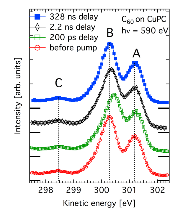
Figure 1 shows the time resolved XPS spectra of the bi-layer system. The red curve and open circles show the XPS spectrum recorded when the X-ray pulse precedes the 532 nm (1 mJ/cm2) pump pulse. The green (open squares), black (open diamonds), and blue curves (full squares) show the XPS probe spectra recorded 200 ps, 2.2 ns, and 328 ns, respectively, after the pump pulse arrival. We note that the optical excitation creates electron hole pairs in the CuPC but not in the C60, as demonstrated in previous UV-Vis absorption experiments of the individual compounds Laurs and Heiland (1987). The vertical dotted (black) lines have been added to guide the eye, indicating the locations of the maxima of the three spectral features for the unperturbed system. The spectra recorded after the pump pulse arrival have been corrected for the surface photovoltage shift (SPV) of the Si substrate, which also shifts the CuPC emission of the deposited film, as discussed in detail below. The curves are offset vertically for improved clarity as indicated by the longer tickmarks. We observe significantly different dynamics for different spectral features. While features A and C are unaffected by the optical excitation, feature B exhibits a distinct time dependent, reversible shift at 200 ps and 2.2 ns delays, and has fully recovered to its original position after 328 ns. Based on earlier XPS studies Kessler (1998) and the spectra of the isolated systems shown in Fig. 2 (I), feature B is largely assigned to the C 1 XPS from C60, superimposed upon a weaker emission feature from CuPC. Features A and C are spectrally pure components of the C 1 XPS from CuPC (Fig. 2 (II)). The time-dependent shift of B upon laser excitation is, therefore, a signature of charge transfer from the chromophore CuPC to the electron acceptor C60. A more detailed picosecond time-resolved investigation of the core photoemission dynamics is in planning, and will be the focus of a future study.
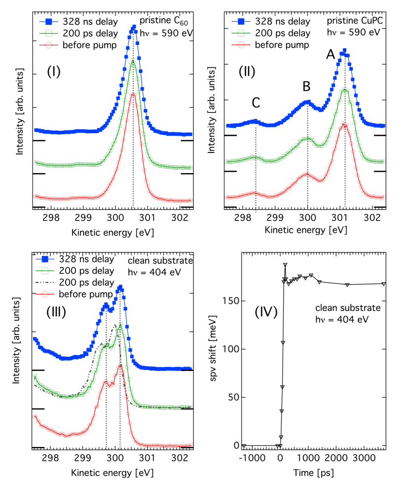
In order to verify the spectral assignments we have conducted several test experiments on pure CuPC films, pure C60 films, and on the bare Si (100) substrate. Figures 2 (I) and (II) show the time-resolved C 1 spectra of thin films of pristine C60 and pristine CuPC, respectively, deposited on pre-cleaned, n-doped Si wafers. Time-resolved Si 2 spectra of the clean Si substrate are shown in Fig. 2 (III). The red curves in Figs. 2 (I),(II),(III) (open circles) show the XPS spectra before the pump pulse arrival, while the green (open squares) and blue curves (full squares) show the probe spectra recorded 200 ps and 328 ns, respectively, after the optical excitation. The peaks in Fig. 2 (II) are labeled following the notation in Kessler (1998). The photoelectron spectra recorded after the pump pulse has arrived at the sample have been corrected for the transient surface photovoltage (SPV) of the Si substrate Long et al. (1990). The baselines of the spectra taken after the pump pulse are shifted vertically as indicated by the longer tickmarks. No changes in the spectral shapes or peak positions beyond the Si SPV response are observed for either of the pristine samples or the clean substrate upon pumping with 532 nm light. For improved clarity, the uncorrected XPS spectrum of the substrate recorded 200 ps after the laser pulse has reached the sample is included as grey, dashed curve in Fig. 2 (III).
Figures 2 (IV) shows the time evolution of the SPV in the clean Si substrate. The SPV is determined by using the Si 2 XPS spectra shown in Fig. 2 (III). The perfect alignment of the corrected spectra corroborates the reproducibility of the measurements and the reliability of the corrections. Upon pumping with the optical laser, a transient SPV of about 160 mV is observed within the response time of the apparatus. Over the timescale of the experiment (3.5 ns) the system relaxes only to a small extent. However, within this time interval, the time dependent shift of peak B in Fig. 1 has almost completely recovered to its initial position, demonstrating that the dynamics of peak B are driven by a different mechanism than the substrate SPV dynamics. Traces recorded for longer pump-probe time delays (not shown) reveal that the surface potential has fully recovered after 3.6 s, i. e. well before the next optical pump pulse arrives.
It is important to emphasize that upon laser irradiation the spectra of the pure films show no other change than the SPV shift of the Si substrate. Apart from this rigid shift, the line shapes and peak positions are identical.
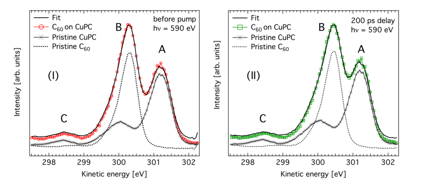
In order to quantify the observed trends in Fig. 1, a component analysis of the time resolved XPS spectra is performed as illustrated in Figs. 3 (I) and (II). They show the XPS spectra of the bi-layer system of C60 on CuPC (open circles, red curve and open squares, green curve) recorded (I) before and (II) 200 ps after the optical excitation, respectively. The color convention is the same as in Fig. 1. The measured spectra can be well described by linear combinations of the spectra of pristine CuPC (stars, black curve) and C60 (dashed black line) spectra, which have been shifted and scaled in a least-squares fit procedure to give the best representation of the time-dependent XPS spectra of the combined system (black full curve) Schlebusch et al. (1996); Schlebusch (1998); Roth et al. (2014). Note that the composite curves describe the experimental results very well despite the simplicity of the four-parameter fits (2 energy shifts and 2 amplitudes).
The analysis shows that the C 1 XPS of CuPC does not change upon optical excitation, whereas the C 1 spectrum of C60 on top of CuPC exhibits a reversible time dependent shift of 144 meV to lower binding energies. This shift is compatible with the presence of an additional negative screening charge on C60, which has been injected from the CuPC.
In other words, upon optical laser pumping, the CuPC molecules are excited and electrons in the HOMO of the CuPC molecules are promoted into an excitonic state, while the C60 molecules are unaffected. However, due to the high electron affinity of the fullerenes, the electrons rapidly move towards the C60 layer, whereby the exciton dissociates to inject an electron into C60 and a hole remains in the CuPC phase. Thus, a large number of electrons have arrived in the C60 layer 200 ps after the optical excitation, and C60 molecules immediately attract an electron from their vicinity upon core ionization. This does not mean that an additional electron is attached to every single C60 molecule, but rather that upon core ionization, efficient core-hole screening is enabled by charge transfer within the C60 or by hopping from neighboring molecules. With increasing time delay occurs a reduction of the free charge carrier concentration, such that, on average, screening of the fullerene core holes is reduced, i. e., the spectral signature of the reduced charge carrier density is an intermediate shift value of the XPS feature B. We, therefore, interpret the intermediate shifts as a superposition of screened and unscreened emission peaks, which are not resolved in our data, and which exhibit time-dependent relative intensities. Once the electron-hole recombination process is complete, the system has returned to its original state as observed before the pump pulse arrival.
Note that a similar shift as observed here for feature B has previously been detected in alkali-doped fullerenes Poirier et al. (1995). In terms of XPS terminology it is predominantly a final state shift. The additional electron density on the C60 is highly mobile and readily screens any core holes, irrespective of their location within the C60 film.
We emphasize that the observed effect does not require one electron to be present on each C60 molecule. The bandwidth of the LUMO of the C60 bilayer is about 500 meV Haddon (1992), whereas the lifetime broadening of a C 1 core hole in C60 is about 70 meV. Accordingly, the charge transfer time within the C60 film is about an order of magnitude faster than the core hole lifetime. This is the reason why electron screening of core holes created in the C60 film is (initially) observed with high probability, and this probability decreases as the total amount of free charge carriers within the C60 film diminishes. The efficient core hole screening by the injected electrons may also indicate a very efficient electron conduction mechanism within the C60 domains, which would be beneficial for PV applications.
We would like to stress that TR-2PPE studies, e. g., by Dutton and Robey Dutton and Robey (2012) and Jailaubekov et al. Jailaubekov et al. (2013) led to the identification of several intramolecular and interfacial excitonic states. A dissociated excitonic state, however, and the timescales for charge transfer to the C60 layer and subsequent recombination across the interface have not yet been unambiguously determined. We expect that TR-XPS studies have the potential to provide critical information in this regard.
At first glance, it is surprising that the CuPC-C 1 XPS spectrum does not exhibit a similarly pronounced shift or shape change as the C60-C 1 line upon charge transfer between the two domains. The optical excitation corresponds to a HOMO-LUMO transition with both orbitals located on the system of the CuPC molecule (i.e., is of character Davidson (1982); Farag (2007)). Therefore, the hole density after charge transfer to the C60 domain, which is expected to be dominated by the original HOMO orbital, should be localized predominantly on the organic phthalocyanine ligands. A possible explanation for the lack of a transient CuPC-C 1 shift may lie in the combination of the particular bi-layer structure of the sample and pinning of the CuPC energy levels to the Si substrate as demonstrated by the Si SPV induced shift of the pristine CuPC XPS spectrum. Further experimental and theoretical work for various sample configurations is planned to test the viability of these assumptions.
The intermolecular charge transfer process in CuPC is more than an order of magnitude slower than in the C60 domain. This estimate is based on angle resolved photoemission data showing a lack of dispersion of the occupied electronic states in ordered CuPC films Kamiya Okudaira et al. (1999). Accordingly, only the molecules containing a hole are expected to show a modified C 1 XPS signal and these modifications may be small, if detectable at all, due to the high localization of the hole densities on single molecules. Further indications that local charge dynamics in CuPC molecules may be challenging to detect are provided by XPS spectra of alkali doped CuPC films Schwieger et al. (2002). They show that the presence of an extra charge on the CuPC molecule is much more readily detected in a shift of the Cu 2 XPS signal, while the shift is hardly observable in the C 1 signal. For a doping level of 1.7 alkali atoms/per CuPC the C 1 shift was reported to be less than 100 meV measured relative to the valence band edge Schwieger et al. (2002). Future studies will include the time-resolved monitoring of Cu inner-shell photolines to gain a more complete picture of charge transfer from both sides of the interface.
The clear spectral signature of the charged C60 phase opens the possibility to directly measure the charge transfer time and to monitor the temporal evolution of the charged state of the electron acceptor. We expect that these dynamic properties of the material blend depend on the electronic structure of the chromophore and on the morphology of the sample, if exciton diffusion plays the dominant role in the charge transfer process. The capability to directly test the correlation between the design of an OPV and the site-specific electron dynamics will be important in optimizing the charge generation and collection processes in a large class of solar energy and light harvesting applications.
Fruitful discussions with D. S. Pemmaraju are gratefully acknowledged. We acknowledge the allocation of beam time at the beam line 11.0.2. of the ALS, as well as the support of the ALS staff during the beam time. The Advanced Light Source is supported by the Director, Office of Science, Office of Basic Energy Sciences, of the U.S. Department of Energy under Contract No. DE-AC02-05CH11231. The Molecular Environmental Sciences beamline 11.0.2 is supported by the Director, Office of Science, Office of Basic Energy Sciences, and the Division of Chemical Sciences, Geosciences, and Biosciences of the US Department of Energy at the Lawrence Berkeley National Laboratory under Contract No. DE-AC02-05CH11231. One of us (WE) would like to thank the ALS for their support and hospitality. OG was supported by the Department of Energy Office of Science Early Career Research Program. SN acknowledges support by the Alexander von Humboldt foundation.
References
- Morita et al. (1992) S. Morita, A. A. Zakhidov, and K. Yoshino, Solid State Commun. 82, 249 (1992).
- Sariciftci et al. (1992) N. S. Sariciftci, L. Smilowitz, A. J. Heeger, and F. Wudl, Science 258, 1474 (1992).
- Schlebusch et al. (1996) C. Schlebusch, B. Kessler, S. Cramm, and W. Eberhardt, Synth. Met. 77, 151 (1996).
- Schlebusch et al. (1999) C. Schlebusch, J. Morenzin, B. Kessler, and W. Eberhardt, Carbon 37, 717 (1999).
- Morenzin et al. (1999) J. Morenzin, C. Schlebusch, B. Kessler, and W. Eberhardt, Phys. Chem. Chem. Phys. 1, 1765 (1999).
- Kessler (1998) B. Kessler, Appl. Phys. A 67, 125 (1998).
- Wilke et al. (2010) A. Wilke, T. Mizokuro, R.-P. Blum, J. P. Rabe, and N. Koch, IEEE J. Sel. Top. Quant. 16, 1732 (2010).
- Schlebusch (1998) C. Schlebusch, Thesis, University of Colgne (1998).
- Gunnarsson et al. (1995) O. Gunnarsson, H. Handschuh, P. S. Bechthold, B. Kessler, G. Ganteför, and W. Eberhardt, Phys. Rev. Lett. 74, 1875 (1995).
- Roth et al. (2014) F. Roth, C. Lupulescu, T. Arion, E. Darlatt, A. Gottwald, and W. Eberhardt, J. Appl. Phys. 115, 033705 (2014).
- Opitz et al. (2013) A. Opitz, J. Frisch, R. Schlesinger, A. Wilke, and N. Koch, J. Electron. Spectrosc. Relat. Phenom. 190, 12 (2013), and references therein.
- Fahlman et al. (2013) M. Fahlman, P. Sehati, W. Osikowicz, S. Braun, M. P. de Jong, and G. Brocks, J. Electron. Spectrosc. Relat. Phenom. 190, 33 (2013), and references therein.
- Kushto et al. (2010) G. Kushto, A. Mäkinen, and P. Lane, IEEE J. Sel. Top. Quant. 16, 1552 (2010).
- Akaike et al. (2010) K. Akaike, K. Kanai, Y. Ouchi, and K. Seki, Adv. Funct. Mater. 20, 715 (2010).
- Koch (2012) N. Koch, Phys. Stat. Sol. (RRL) 6, 277 (2012).
- Li et al. (2014) W. Li, H. Yu, J. Zhang, Y. Yao, C. Wu, and X. Hou, J. Phys. Chem. C 118, 11928 (2014).
- Castet et al. (2014) F. Castet, G. D’Avino, L. Muccioli, J. Cornil, and D. Beljonne, Phys. Chem. Chem. Phys. 16, 20279 (2014).
- Beltran et al. (2014) J. Beltran, F. Flores, and J. Ortega, Phys. Chem. Chem. Phys. 16, 4268 (2014).
- Sai et al. (2012) N. Sai, R. Gearba, A. Dolocan, J. R. Tritsch, W.-L. Chan, J. R. Chelikowsky, K. Leung, and X. Zhu, J. Phys. Chem. Lett. 3, 2173 (2012).
- Dutton and Robey (2012) G. J. Dutton and S. W. Robey, J. Phys. Chem. C 116, 19173 (2012).
- Jailaubekov et al. (2013) A. E. Jailaubekov, A. P. Willard, J. R. Tritsch, W.-L. Chan, N. Sai, R. Gearba, L. G. Kaake, K. J. Williams, K. Leung, P. J. Rossky, and X.-Y. Zhu, Nat. Mater 12, 66 (2013).
- Bluhm et al. (2006) H. Bluhm, K. Andersson, T. Araki, K. Benzerara, G. Brown, J. Dynes, S. Ghosal, M. Gilles, H.-C. Hansen, J. Hemminger, A. Hitchcock, G. Ketteler, A. Kilcoyne, E. Kneedler, J. Lawrence, G. Leppard, J. Majzlam, B. Mun, S. Myneni, A. Nilsson, H. Ogasawara, D. Ogletree, K. Pecher, M. Salmeron, D. Shuh, B. Tonner, T. Tyliszczak, T. Warwick, and T. Yoon, J. Electron. Spectrosc. Relat. Phenom. 150, 86 (2006).
- Neppl et al. (2014) S. Neppl, A. Shavorskiy, I. Zegkinoglou, M. Fraund, D. S. Slaughter, T. Troy, M. P. Ziemkiewicz, M. Ahmed, S. Gul, B. Rude, J. Z. Zhang, A. S. Tremsin, P.-A. Glans, Y.-S. Liu, C. H. Wu, J. Guo, M. Salmeron, H. Bluhm, and O. Gessner, Faraday Discuss. 171, 219 (2014).
- Glover et al. (2001) T. Glover, G. Ackermann, A. Belkacem, B. Feinberg, P. Heimann, Z. Hussain, H. Padmore, C. Ray, R. Schoenlein, and W. Steele, Nucl. Instrum. Methods Phys. Res. Sec. A 467, 1438 (2001).
- Laurs and Heiland (1987) H. Laurs and G. Heiland, Thin Solid Films 149, 129 (1987).
- Long et al. (1990) J. P. Long, H. R. Sadeghi, J. C. Rife, and M. N. Kabler, Phys. Rev. Lett. 64, 1158 (1990).
- Poirier et al. (1995) D. M. Poirier, D. W. Owens, and J. H. Weaver, Phys. Rev. B 51, 1830 (1995).
- Haddon (1992) R. C. Haddon, Acc. Chem. Res. 25, 127 (1992).
- Davidson (1982) A. T. Davidson, J. Chem. Phys. 77, 168 (1982).
- Farag (2007) A. A. M. Farag, Opt. Las. Tech. 39, 728 (2007).
- Kamiya Okudaira et al. (1999) K. Kamiya Okudaira, S. Hasegawa, H. Ishii, K. Seki, Y. Harada, and N. Ueno, J. Appl. Phys. 85, 6453 (1999).
- Schwieger et al. (2002) T. Schwieger, H. Peisert, M. S. Golden, M. Knupfer, and J. Fink, Phys. Rev. B 66, 155207 (2002).