Tight binding analysis of Si and GaAs ultra thin bodies with subatomic resolution
Abstract
Empirical tight binding(ETB) methods are widely used in atomistic device simulations. Traditional ways of generating the ETB parameters rely on direct fitting to bulk experiments or theoretical electronic bands. However, ETB calculations based on existing parameters lead to unphysical results in ultra small structures like the As terminated GaAs ultra thin bodies(UTBs). In this work, it is shown that more reliable parameterizations can be obtained by a process of mapping ab-initio bands and wave functions to tight binding models. This process enables the calibration of not only the ETB energy bands but also the ETB wave functions with corresponding ab-initio calculations. Based on the mapping process, ETB model of Si and GaAs are parameterized with respect to hybrid functional calculations. Highly localized ETB basis functions are obtained. Both the ETB energy bands and wave functions with subatomic resolution of UTBs show good agreement with the corresponding hybrid functional calculations. The ETB methods can then be used to explain realistically extended devices in non-equilibrium that can not be tackled with ab-initio methods.
I Introduction
Modern semiconductor nanodevices have reached critical device dimensions in the sub-10 nanometer range. These devices consist of complicated two or three dimensional geometries and are composed of multiple materials. Confined geometries such as ultra thin body (UTB)Choi et al. (2000), FinFETsHisamoto et al. (2000) and nanowiresXuan et al. (2006) structures are usually adopted in nanometer scale device designs to obtain desired performance characteristics.Most of the electrically conducting devices are not arranged in infinite periodic arrays, but are of finite extent with contacts controlling the current injections and potential modulation. Typically, there are about 10000 to 10 million atoms in the active device region with contacts controlling the current injection. These finite sized structures suggest an atomistic, local and orbital-based electronic structure representation for device level simulation. Quantitative device design requires the reliable prediction of the materials’ band gaps and band offsets within a few meV and important effective masses within a few percent in the geometrically confined active device regions. ETB model is usually fitted to bulk dispersions without any definition of the spatial wave function details. However, recent ab-initio study of UTBs Hatcher and Bowen (2013) showed that the surface carrier distribution in confined systems is strongly geometry and material dependent. This suggests that the charge distribution for realistic predictions of nanodevice performances should be resolved with subatomic resolution.
Ab-initio methods offer atomistic representations with subatomic resolution for a variety of materials. However, accurate ab-initio methods, such as Hybrid functionals Krukau et al. (2006), GW Hybertsen and Louie (1986) and BSE approximations Ismail-Beigi and Louie (2003) are in general computationally too expensive to be applied to systems containing millions of atoms. Furthermore, those methods assume equilibrium and cannot truly model out-of-equilibrium device conditions where e.g. a large voltage might have been applied to drive carriers. The ETB methods are numerically much more efficient than Ab-initio methods. ETB has established itself as the standard state-of-the-art basis for realistic device simulations. It has been successfully applied to electronic structures of millions of atoms Klimeck et al. (2002) as well as on non-equilibrium transport problems that even involve inelastic scattering. Lake et al. (1993)The accuracy of the ETB methods depend critically on the careful calibration of the empirical parameters. The traditional way to determine the ETB parameters is to fit ETB band structures to experimental data of bulk materials. Jancu et al. (1998); Boykin et al. (2002)
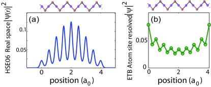
The ETB basis functions remain implicitly defined during traditional fitting processes. The lack of explicit basis functions makes it difficult to predict wave function dependent quantities like optical matrix elements with high precision. More importantly, ETB models parameterized by traditional fitting processes suffer from potential ambiguity when applied to ultra small structures such as UTBs, nanowires and more complicated geometries. For instance, the existing ETB parameters of GaAs Boykin et al. (2002) applied to a As terminated GaAs UTB with an implicit Hydrogen passivation model Lee et al. (2004) results in unphysical top valence band states as shown in Fig. 1: The real space probability amplitudes of ab-initio topmost valence bands correspond to confined states with the probability amplitude peaking in the center of the UTB rather than the surface of the UTB as in ETB.In Fig. 1, the hybrid functional calculations include Hydrogen atoms explicitly whereas the ETB calculations include only their impact implicitly. Lee et al. (2004) The mismatch between the envelopes of ETB and ab-initio wavefunctions suggests a calibration of wave functions in the ETB parameterization process is necessary. It is also found that the method of passivation (i.e. implicit or explicit inclusion of Hydrogen atoms) has an effect on the nature of the valence band states.
.
Therefore, a more fundamental fitting process that relates both the band structure and the wave functions of ETB models with ab-initio calculations is desirable. Existing approaches to construct localized basis functions and tightbinding-like Hamiltonians from ab-initio results include maximally localized Wannier functions(MLWF), Marzari and Vanderbilt (1997); Souza et al. (2001) quasi-atomic orbitals, Qian et al. (2008); Lu et al. (2004) or DFT-TB analysis. Urban et al. (2011)The MLWFs are constructed using Bloch states of either isolated bands Marzari and Vanderbilt (1997) or entangled bands. Souza et al. (2001)These methods typically include interatomic interactions beyond first nearest neighbors. However, these methods do not eliminate the above discussed ambiguity of the commonly used orthogonal sp3d5s* ETB models. Furthermore, these approaches usually disregard excited orbitals which are often needed to correctly parameterize semiconductors conduction bands. In previous work, it was already suggested how to generate ETB parameters that are compatible with typical ETB models and still reproduce ab-initio results. Tan et al. (2013)This previous method was already applied to several materials such as GaAs, MgO Tan et al. (2013) and SmSe Jiang et al. (2013) and yielded a good agreement between bulk ETB and ab-initio band structures. However, the resulting wave functions did not satisfactorily agree with the ab-initio wave functions.
In this paper, an improved algorithm of Ref. Tan et al., 2013 is presented that ”maps” ab-initio results (i.e. eigenenergies and eigenfunctions) to tight binding models. Compared with the previous workTan et al. (2013), the presented method allows much better agreement of the ETB and ab-initio wave functions. In this present mapping algorithm, rigorous, wavefunction-derived ETB parameters for the Hamiltonian, for highly localized basis functions, and for explicit surface passivation are obtained. It is important to mention that the ETB Hamiltonian of this method can be limited to first nearest neighbor interaction. The mapping process is applied to both bulk Si and GaAs to generate ETB parameters and explicit basis functions from corresponding hybrid functional calculations. It is demonstrated in this work, that the wave-function derived ETB Hamiltonian does not yield the ambiguity discussed with Fig. 1. In the same way, the transferability of the ETB model to nanostructures is improved. This is demonstrated by a comparison of ETB and Hybrid functional results in GaAs and Si UTBs.
This paper is organized as follows. In section II, the algorithm of parameter mapping from ab-initio calculations to tight binding models is described. Section III shows the application of the mapping algorithm to bulk and UTB systems. Subsection III.1 presents the application of the present algorithm to bulk Si and GaAs. Bulk band structures and realspace basis functions are shown and discussed there as well. Subsection III.2 shows the application of the algorithm to UTB systems and compares ETB band structures and wave functions with corresponding ab-initio results. The algorithm and its results are summarized in Section IV.
II Method
II.1 Parameter Mapping Algorithm
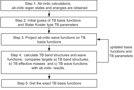
The algorithm of the parameter mapping from ab-initio results to ETB models is shown in Fig. 2.As will be shown in the following, the ETB parameters and basis functions are obtained in an iterative fitting procedure that spans over 5 steps (with steps 3 through 4 being iterated). The resulting 1st nearest neighbor Hamiltonian is of Slater Koster table type. Slater and Koster (1954); Podolskiy and Vogl (2004) The resulting basis is composed of orthonormal real space functions which have the shape (vectors are given in bold type)
| (1) | |||||
Here, labels the atom type, whereas the , and are principle, angular and magnetic quantum numbers, respectively. All materials considered in this work contain no magnetic polarization. Therefore, the basis functions are spin independent. The tesseral spherical harmonics describe the dependence of the basis functions on the angular coordinates and . The functions and define the radial dependence of the basis functions. The contribution of to the basis functions is much smaller than the contribution of . The detailed shapes of the radial functions and are subject to the fitting algorithm.
.
Step 1: First, electronic band structures and wave functions are solved which serve as fitting targets to the overall mapping algorithm
| (2) |
The index corresponds to the band index and represents a momentum vector in the first Brillouin zone. In principle, any method that is capable of solving band diagrams and explicit basis functions can provide these fitting targets. Throughout this work, however, hybrid functional calculations are performed for step 1. Kim et al. (2009)
Step 2: In the second step, initial guesses for the ETB basis functions and ETB parameters are defined. During the fitting process, the ETB basis is spanned by non-orthogonal functions given by
| (3) |
The in Eq. (3) differ from the of the final basis functions in Eq. (1). The details of the initial guesses for the diagonal and off-diagonal elements of the Hamiltonian are not essential for the overall algorithm. Nevertheless, initial guesses that follow the framework of existing ETB parameter sets improve the overall fitting convergence. Urban et al. and Lu et al. discuss that interactions up to third nearest neighbors might be needed to exactly reproduce ab-initio results. Urban et al. (2011); Lu et al. (2004)In contrast, we find that the interatomic interaction elements of can be limited to first nearest neighbor interactions throughout this work while still reproducing ab-initio results very well.
Step 3: The nonorthogonal basis functions in position space are transformed into the Bloch representation Ashcroft and Mermin (1976)
| (4) | |||||
where is the position of atom type in the unit cell and the sum runs over all unit cells of the system with , the position of the respective cell. To improve readability of all formulas in the Dirac notation, the indices of atom type and quantum numbers are merged into Greek indices . For the further steps, an orthogonal basis is created out of the basis with Löwdin’s symmetrical orthogonalization algorithm. Lowdin (1950)Since steps 4 and 5 are formulated in the basis , the wave functions of step 1 must be transformed into this basis
| (5) |
where
| (6) |
with the projection operator
| (7) |
Equation (5) contains an approximation of the ab-initio wave functions in so far that the sum over extends only over those orbitals that are included in the tight binding basis . This basis and of similar ETB models have much fewer basis vectors than the input ab-initio calculation. This rank reduction is a typical outcome of rectangular transformations such as and is well known in the field of low rank approximations Zeng et al. (2013).
Step 4: Here, the quality of the ETB fitting is assessed. In this step, the band structures of the current ETB model and the ab-initio input are compared. If these sufficiently agree, the phases of the ETB wave functions are modulated to agree with the ab-initio ones and both wave functions are compared after that. The ETB Hamiltonian of step 2 is diagonalized in the basis of step 3 to obtain ETB band structures and eigen vectors
| (8) |
with
| (9) |
To assess the quality of the ETB results is assessed, different fitness functions , and are defined for energies, masses and wave functions respectively. The and are given by
| (10) | |||||
| (11) |
where and are weights defined for each target.
As a convention for wave functions phases, another set of ETB wave functions is introduced
| (12) |
The unitary transformation is defined by
| (13) |
with
| (14) |
Here, the sum over and runs over all ETB states and ab-initio states with equivalent energies . With this transformation, the equation holds
| (15) |
for equivalent states. This phase adaption can only work if the ETB band structure is close enough to the ab-initio result. The ETB wave function fittness is given by
| (16) |
The weights are varying depending on respective fitting focusses. Deviations of from have in general two reasons: inadequate basis functions and/or eigenfunctions of a poorly approximated ETB Hamiltonian. Therefore, can be estimated as
| (17) |
The first right hand side term of the last equation describes the deviation of the low-rank approximated ab-initio wave functions. This becomes obvious with the projector property
| (18) |
The second term on the right hand side of Eq. (17) contains information about the quality of the eigenfunctions of the approximate ETB Hamiltonian . This is understandable when Eqs. (5) and (12) are inserted into this term
| (19) |
The fitness function represents the major improvement over the traditional ETB eigenvalue fitting (e.g. typically limited to energies and effective masses). All fitness functions are minimized by iterating over the steps 3 and 4: the Slater Koster type parameters for the ETB Hamiltonian and the parameters of the radial ETB basis functions are adjusted for every iteration of step3.
Step 5: Once the fitness functions are small enough to cease the iterations, it is assumed that those eigenfunctions of the ETB Hamiltonian that were subject to the fitting are identical to the eigenfunctions of the ab-initio Hamiltonian after a transformation
| (20) |
This transformation is determined by a singular value decomposition of the rectangular overlap matrix of ab-initio eigenstates with ETB eigenstates
| (21) |
The row index runs over all ab-initio eigenstates - exceeding those that served as fitting targets, whereas the column index covers all the ETB eigenfunctions. The and are square and is a rectangular matrix. The transformation is then defined as
| (22) |
is constructed from relevant columns of a unitary transformation. Combining Eqs. (20) and (9) allows to determine the Bloch periodic final basis functions
| (23) |
The real space counterpart of is given by
| (24) |
III Results
In this work, ab-initio level calculations of Si and GaAs systems were performed with VASP Kresse and Furthmuller (1996). The HSE06 hybrid functional Kim et al. (2009) is used to produce reasonable band gaps in both the bulk and the UTB cases. In all HSE06 calculations, a cutoff energy of 350eV is used. -point centered Monkhorst Pack kspace grids are used for both bulk and UTB systems. The size of the kspace grid for bulk calculations is a , while one for UTB is . k-points with integration weights equal to zero are added to the original or grids in order to generate energy bands with higher k-space resolution. The spin orbit coupling is included in band structure calculations. Small hydrostatic strains up to are introduced to adjust the bulk band gaps in order to match experimental results. The lattice const used in this work is given by table 1.
III.1 Application to Bulk Materials
| Si | GaAs | ||||||||||||||||||||||||||||||||||||||||||||||||||||||||||||||||||||||||||||||||||||||||||||||||||||||||||||||||||||||||
|---|---|---|---|---|---|---|---|---|---|---|---|---|---|---|---|---|---|---|---|---|---|---|---|---|---|---|---|---|---|---|---|---|---|---|---|---|---|---|---|---|---|---|---|---|---|---|---|---|---|---|---|---|---|---|---|---|---|---|---|---|---|---|---|---|---|---|---|---|---|---|---|---|---|---|---|---|---|---|---|---|---|---|---|---|---|---|---|---|---|---|---|---|---|---|---|---|---|---|---|---|---|---|---|---|---|---|---|---|---|---|---|---|---|---|---|---|---|---|---|---|---|
|
|
|
||||||||||||||||||||||||||||||||||||||||||||||||||||||||||||||||||||||||||||||||||||||||||||||||||||||||||||||||||||||||
|
|
|
For bulk Si and GaAs, fitting targets include the band structures of the lowest 16 bands (with spin degeneracy) along high symmetry directions, important effective masses and wave functions at high symmetry points such as , and points. ETB basis functions in real space is reconstructed on center k space grid using Eq (24).
| Si | |||||||||||||||||||||||||||||||||||||||||||||||||||||||||||||||||||||||||||||||||
|---|---|---|---|---|---|---|---|---|---|---|---|---|---|---|---|---|---|---|---|---|---|---|---|---|---|---|---|---|---|---|---|---|---|---|---|---|---|---|---|---|---|---|---|---|---|---|---|---|---|---|---|---|---|---|---|---|---|---|---|---|---|---|---|---|---|---|---|---|---|---|---|---|---|---|---|---|---|---|---|---|---|
|
|
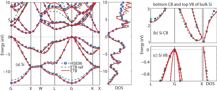
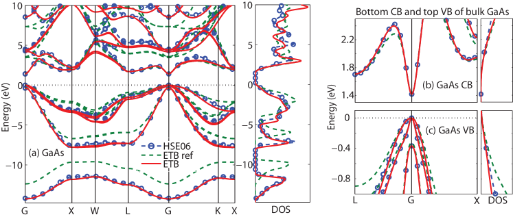
The band structures and DOS of bulk Si and GaAs (HSE06 vs ETB) are shown in Fig. 3 and 4 respectively. The band structures using existing Si and GaAs ETB parametersBoykin et al. (2004, 2002) are also shown in corresponding figures. The ETB band structures and DOS using parameters generated by this work show better agreement with the corresponding hybrid functional results compared with the existing parameterizations. For bulk Si, the existing parameterization shows a unexpected low band around 5 eV above topmost valence bands. In the traditional fitting process, the band shows a strong preference for moving downward Boykin et al. (2004). Due to large number of parameters to be determined, traditional (energy-gap and effective-mass) based fitting procedures can find local minima in their fitness functions corresponding to wave functions significantly different from those predicted by ab-initio methods. The present method has the important advantage that optimization involves not only masses and gaps but also wavefunctions. Thus the ETB wavefunctions can be kept close to their ab-initio counterparts. For GaAs, the existing parameterization shows 2 eV higher -type low lying valence bands. The ETB parameters of bulk Si and GaAs are listed in table 1. It can be seen from tables 2 and 3, the anisotropic hole masses by ETB show a remarkable agreement with HSE06 results. The principal authors of the previous worksBoykin et al. (2002, 2004) explicitly pointed out that fitting hole masses had been very difficult with the previous methods.
| GaAs | ||||||||||||||||||||||||||||||||||||||||||||||||||||||||||||||||||||||||||||||||||||||||||||||||||||||||||
|---|---|---|---|---|---|---|---|---|---|---|---|---|---|---|---|---|---|---|---|---|---|---|---|---|---|---|---|---|---|---|---|---|---|---|---|---|---|---|---|---|---|---|---|---|---|---|---|---|---|---|---|---|---|---|---|---|---|---|---|---|---|---|---|---|---|---|---|---|---|---|---|---|---|---|---|---|---|---|---|---|---|---|---|---|---|---|---|---|---|---|---|---|---|---|---|---|---|---|---|---|---|---|---|---|---|---|
|
|
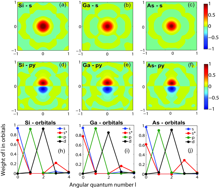
The orthogonal ETB basis functions of Si, Ga and As atoms are shown in Fig. 5. The ETB basis functions are slightly environment dependent because they are orthogonal. Thus the ETB basis functions are not invariant under arbitrary rotations but invariant under symmetry operations within group, as pointed out by Slater and Koster Slater and Koster (1954). It can be seen from Fig. 5.(a) to (f) that the and orbitals show and features near the atom. More complicated patterns in the area further away from the atom can be observed. These complicated patterns correspond to components with high angular momentums. The feature of orthogonal ETB basis function resembles the augmented basis functions used in ab-initio level calculations such as Augmented Plane Waves(APWs) and Muffin Tin Orbitals(MTOs). The orthogonal ETB basis functions have multiple angular parts in each orbital as shown by Fig. 5.(g),(h) and (i). The , and type ETB basis functions are dominated by components with , and respectively. More than for the , and orbitals are comprised of their , and components respectively. The excited type ETB basis functions have higher angular momentum and the components have contributions of to . The second largest contribution in orbitals is the component with . The component attached to the orbitals have angular part equivalent to real space function . This is a result of the existence of -like crystal field near each atom in zincblende and diamond structures.
III.2 Application to UTBs
To validate the transferability of the ETB model, band structures and eigen functions of [001] UTBs passivated by Hydrogen atoms are calculated by both HSE06 and ETB models. The current calculations assume no strain in the UTBs. In the HSE06 calculations, charged hydrogen atoms are used to passivate the dangling bonds of the surface atoms in GaAs UTBs. The surface As and Ga atoms are passivated by charged hydrogen atoms with 3/4 ( denoted by ) and 5/4 ( denoted by ) electron respectively. The charged hydrogen atoms neutralize most of the surface induced electric field in the UTBs. As a result, the charge distribution and local potential shows almost flat envelopes inside the UTBs. Small deviation of potential can only be observed at the surface Si/Ga/As atoms. The nearly flat potential envelope suggests geometry dependent build-in potentials are needed only for surface atoms. Thus the comparisons between self-consistent hybrid functional calculations and single shot ETB calculations are fair.
The HSE06 calculations show that the Hydrogen orbitals contribute to the deep valence bands, thus Hydrogen atoms are considered explicitly into the ETB Hamiltonian of UTBs in this work. 1s orbital is used as the ETB basis function for Hydrogen atoms. The explicit passivation model include extra Slater Koster type ETB parameters , , , and . Further more, a geometry and element dependent potential is included for surface atoms. The onsite energies of the surface atoms are shifted by . The onsite energy of the surface Ga atoms are thus ; and for surface As atoms, the onsite energies are . Here the stands for ,, and orbitals. ETB parameters of Si/GaAs in Si/GaAs UTBs are identical with the parameters of unstrained bulk materials provided in section III.1.
To determine the ETB parameters of H-passivation, band structures and real space wave functions of selected bands near the Fermi level of the UTBs are considered as fitting targets. The inclusion of wave functions as targets serves the purpose of correcting possible problematic states. The target Si/GaAs UTBs contain 17 non-Hydrogen atomic layers. Parameters for Hydrogen atoms are also shown in table 1. In GaAs UTBs, As and Ga are passivated by Hydrogen atoms with different charge, thus the Hydrogen atoms have different onsite energies when different types of atoms are passivated. The Hydrogen atoms bonding with As atoms are charged positively while the ones bonding with Ga atoms are charged negatively. Consequently, the which forms bond with As have a higher onsite energy than the which forms bond with Ga.
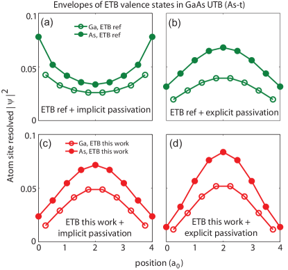
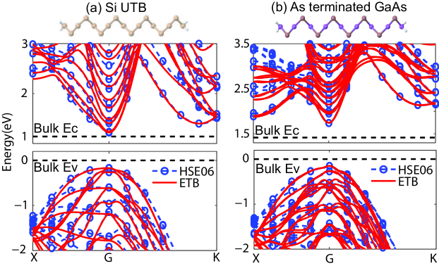
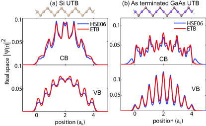
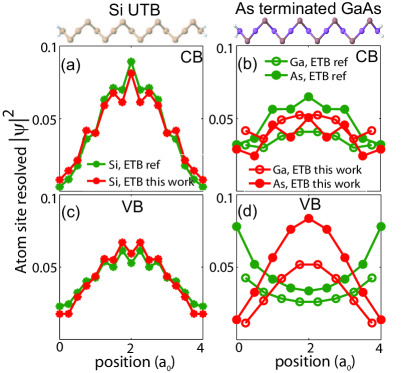
Band structures of Si/GaAs UTBs are shown in Fig. 6. The ETB band structures match the HSE06 band structures well for energies ranging from 1eV below the topmost valence bands to 1eV above the lowest conduction bands. Using the explicit ETB basis functions, ETB wave functions of UTBs with subatomic resolution are obtained and can be compared with corresponding HSE06 wave functions. Planar averaged probability amplitudes of wave functions of the lowest conduction band and top most valence bands in Si/GaAs UTBs are shown in Fig. 7. It can be seen that not only the envelope but also details in subatomic resolution of the ETB planar averaged show agreement with corresponding HSE06 results. On the other hand, Fig. 8 compares the ETB atom site resolved probability amplitudes among ETB models in present and previous works (Ref. Boykin et al., 2004, 2002). The cations and anions in GaAs UTBs form different envelopes for all of the presented states. The lowest conduction and highest valence states turn out to be well confined states in Si UTBs in all of the calculations. While, in GaAs UTBs, the lowest conduction states has significant contribution from the surface atoms. In Si ETB probability amplitudes by previous parametrizations show similar envelopes compared to the ETB and HSE06 probability amplitudes in this work. Fig. 8 (d) shows the problematic valence states in As terminated GaAs UTB by parameters of previous work. The corresponding valence states by this work turn out to be a well confined ones. To investigate this issue in more detail, in Fig. 9, ETB atom site resolved probability amplitudes for the topmost valence states of the four possible As-terminated GaAs UTBs are plotted: (a) previous parameters Boykin et al. (2002) and implicit passivation Lee et al. (2004); (b) previous parameters and explicit passivation; (c) new parameters and implicit passivation; (d) new parameters and explicit passivation. It is clear that, for a given set of bulk parameters, the implicit passivation model leads to wavefunctions that are less-confined than those of the explicit passivation model. On the other hand, with the same passivation model, the ETB parameters by this works shows more confined top valence states than the existing ETB parameters. Thus the un-confined ETB state using the existing parameter set and implicit passivation model appears to be due to both the bulk GaAs parameters and the passivation model. The implicit modelLee et al. (2004) replaces the - and -orbitals of the surface atoms by sp3 hybrids and raises the energy of the dangling hybrids by . The - and -orbitals are left completely un-passivated, and the unconfined states of Fig. 9 (a) are only slightly affected by changing the value of . The impact of alternate implicit passivation model to explicit passivation model is obvious by comparing sub-figures (a) to (b), as well as (c) to (d). To better understand the role of bulk parameters to this behavior, we experimented by reducing the magnitude of the nearest-neighbor - coupling parameters in both sets as , . Remarkably, in both cases the topmost valence-band state became much more confined. Bulk valence band wave functions in modified and original parameter sets tell the story: The general trend is that bulk sets which generate more -like top of VB states give better confinement under passivation (and especially implicit passivation) than do those with higher d-content. The reduction of and lead to more -like top VB states. Ga terminated case has less passivation problems because its top-of-VB bulk states have more contribution from the As atoms than from the Ga atoms.
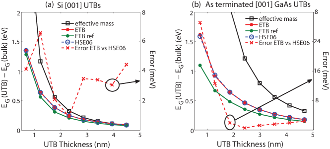
Fig. 10 shows the band gaps of the Si and GaAs [001] UTBs as functions of UTB thickness. With the ETB parameters by this work, the ETB bandgaps of Si and GaAs UTBs with thickness from 0.5nm to 4nm agree well with the gaps by HSE06 calculations. The ETB bandgaps of Si UTBs using parameters from previous work also show good agreement with the HSE06 results. However the ETB bandgaps of GaAs UTBs using parameters from previous work and implicit passivation model are of around lower than the Hybrid functional results. The gaps of GaAs UTBs terminated with Ga and As atoms are very close in value for both Hybrid functional and ETB results in this work, however the gaps of GaAs UTBs terminated with Ga and As atoms by previous parameterizations and implicit passivation model show 0.1 to 0.2eV discrepancies. The band gap change in Si UTBs thicker than 3nm can be model by effective mass model( assuming parabolic E-k relation ). While in the GaAs UTBs, the discrepancies between effective mass calculations and HSE06 or TB calculations are obvious for all GaAs UTBs presented, suggesting the non-parabolic feature of the GaAs valleys have significant impact to GaAs nano structures. The gaps by previous parameterization with implicit passivation model of As terminated GaAs UTBs has lower confined energies due to the unconfined valence states.
IV Conclusion
It has been shown that the existing ETB parameterization together with the implicit passivation model gives unphysical states in As terminated GaAs UTB calculations. A more reliable technique of ab-initio mapping which generates ETB parameters and basis functions from ab-initio is developed. The ab-initio mapping process is applied to both bulk Si and GaAs. Slater Koster type ETB parameters within 1st nearest neighbour approximation and highly localized ETB basis functions are obtained. The ETB parameters and basis functions of Si and GaAs are validated in corresponding UTB systems with passivation models that consider Hydrogen atom explicitly. Band gaps in Si and GaAs UTBs with different thickness are also calculated by HSE06, ETB and effective mass model. Compared with the existing ETB parameterizations and implicit passivation model, the ETB calculations in this work show good agreements with HSE06 calculations in both band structures and wave functions. This work shows that the ETB parameters by ab-initio mapping have good transferability. The mapping method developed here significantly reduces the uncertainty in both bulk and passivation models.
Acknowledgements.
nanoHUB.org computational resources operated by the Network for Computational Nanotechnology funded by NSF are utilized in this work. Evan Wilson from Network for Computational Nanotechnology, Purdue University is acknowledged for improving the manuscript.References
- Choi et al. (2000) Y. K. Choi, K. Asano, N. Lindert, V. Subramanian, T. J. King, J. Bokor, and C. Hu, IEEE Electron Device Lett 21, 254 (2000).
- Hisamoto et al. (2000) D. Hisamoto, C. Lee, W, J. Kedzierski, H. Takeuchi, K. Asano, C. Kuo, E. Anderson, J. King, T, J. Bokor, and C. Hu, IEEE Electron Device Lett 24, 2320 (2000).
- Xuan et al. (2006) Y. Xuan, W. Lu, Y. Hu, H. Yan, and M. Lieber, C, Nature 441, 489 (2006).
- Hatcher and Bowen (2013) R. Hatcher and C. Bowen, Applied. Phys. Let 103, 162107 (2013).
- Krukau et al. (2006) A. Krukau, O. Vydrov, A. Izmaylov, and G. Scuseria, J. Chem. Phys. 124, 224106 (2006).
- Hybertsen and Louie (1986) M. S. Hybertsen and S. G. Louie, Phys. Rev. B 34, 5390 (1986).
- Ismail-Beigi and Louie (2003) S. Ismail-Beigi and S. G. Louie, Phys. Rev. Lett. 90, 076401 (2003).
- Klimeck et al. (2002) G. Klimeck, F. Oyafuso, T. B. Boykin, C. R. Bowen, and P. V. Allmen, Computer Modeling in Engineering and Science (CMES) 3, 601 (2002).
- Lake et al. (1993) R. Lake, G. Klimeck, and S. Datta, Phys. Rev. B 47, 6427 (1993).
- Jancu et al. (1998) J.-M. Jancu, R. Scholz, F. Beltram, and F. Bassani, Phys. Rev. B 57, 6493 (1998).
- Boykin et al. (2002) T. B. Boykin, G. Klimeck, R. C. Bowen, and F. Oyafuso, Phys. Rev. B 66, 125207 (2002).
- Lee et al. (2004) S. Lee, F. Oyafuso, P. von Allmen, and G. Klimeck, Phys. Rev. B 69, 045316 (2004).
- Marzari and Vanderbilt (1997) N. Marzari and D. Vanderbilt, Phys. Rev. B 56, 12847 (1997).
- Souza et al. (2001) I. Souza, N. Marzari, and D. Vanderbilt, Phys. Rev. B 65, 035109 (2001).
- Qian et al. (2008) X. Qian, J. Li, L. Qi, C.-Z. Wang, T.-L. Chan, Y.-X. Yao, K.-M. Ho, and S. Yip, Phys. Rev. B 78, 245112 (2008).
- Lu et al. (2004) W. C. Lu, C. Z. Wang, T. L. Chan, K. Ruedenberg, and K. M. Ho, Phys. Rev. B 70, 041101 (2004).
- Urban et al. (2011) A. Urban, M. Reese, M. Mrovec, C. Elsässer, and B. Meyer, Phys. Rev. B 84, 155119 (2011).
- Tan et al. (2013) Y. Tan, M. Povolotskyi, T. Kubis, Y. He, Z. Jiang, G. Klimeck, and T. Boykin, Journal of Computational Electronics 12, 56 (2013), ISSN 1569-8025.
- Jiang et al. (2013) Z. Jiang, M. A. Kuroda, Y. Tan, D. M. Newns, M. Povolotskyi, T. B. Boykin, T. Kubis, G. Klimeck, and G. J. Martyna, Applied Physics Letters 102, 193501 (2013), ISSN 0003-6951.
- Slater and Koster (1954) J. C. Slater and G. F. Koster, Phys. Rev. 94, 1498 (1954).
- Podolskiy and Vogl (2004) A. V. Podolskiy and P. Vogl, Phys. Rev. B 69, 233101 (2004).
- Kim et al. (2009) Y.-S. Kim, K. Hummer, and G. Kresse, Phys. Rev. B 80 035203 (2009).
- Ashcroft and Mermin (1976) N. Ashcroft and N. Mermin, Solid State Physics (Saunders College, Philadelphia, 1976).
- Lowdin (1950) P.-O. Lowdin, J. Chem. Phys. 18, 56 (1950), ISSN 365.
- Zeng et al. (2013) L. Zeng, Y. He, M. Povolotskyi, X. Liu, G. Klimeck, and T. Kubis, Journal of Applied Physics 113, 213707 (2013).
- Kresse and Furthmuller (1996) G. Kresse and J. Furthmuller, Computational Materials Science 6, 15 (1996).
- Boykin et al. (2004) T. B. Boykin, G. Klimeck, and F. Oyafuso, Phys. Rev. B 69, 115201 (2004).