Linear Amplification of Optical Signal in Coupled Photonic Crystal Waveguides
Abstract
We introduce a weakly coupled photonic crystal waveguide as a promising and realistic model for all-optical amplification. A symmetric pillar type coupled photonic crystal waveguide consisting of dielectric rods periodically distributed in a free space is proposed as all-optical amplifier. Using the unique features of the photonic crystals to control and guide the light, we have properly chosen the frequency at which only one mode (odd mode) becomes the propagating mode in the coupled photonic crystal waveguide, whereas another mode (even mode) is completely reflected from the guiding structure. Under this condition, the all-optical amplification is fully realized. The amplification coefficient for the continuous signal and the Gaussian pulse is calculated.
Index Terms:
All-optical devices, Photonic crystals, Optical amplifiersI Introduction
Photonic bandgap crystals are artificial dielectric or metallic structures in which any electromagnetic wave propagation is forbidden within a fairly large frequency range. A photonic crystal with a complete bandgap could be used to localize electromagnetic waves to specific arrays, to guide and control the propagation of the waves along certain directions at restricted frequencies [1, 2]. Photonic crystal waveguide (PCW) can be made by removing a row of either air columns or dielectric rods that result in multimode guiding [3]. PCWs devices are very promising candidates for all optical telecommunication purposes due to the absence of energy losses and their ability for strong light confinement [4, 5]. If PCWs are placed in a close proximity, a coupled PCW is formed and the optical power is efficiently transferred from one PCW to another. Recently, the coupled PCWs have received much attention because of their promising applications to ultra-compact, miniaturized photonic devices such as filters, switches, power dividers, and couplers.
In the manuscript we propose two weakly coupled PCWs as promising and realistic experimental model for all-optical amplification. Our idea of amplification of the optical signals in two weakly coupled PCWs is based on the possibility of coexistence of two (even and odd) fundamental modes, which have different propagation properties at the same frequency. Particularly, if the light is launched into two coupled PCWs at some particular frequency properly chosen, only one mode becomes a propagating mode, whereas another mode is completely reflected from the system and its carried power flux is exactly zero. The operating setup is quite similar to the Y-junction type waveguide analyzed in a detail in [6]. The novelty of our work is that we give a deep physical insight into the realization of the optical signal amplification in such a guiding system. It should be emphasized that all the scenarios of all-optical amplification considered in the manuscript are completely linear, thus there is no need for implementation of nonlinear effects.
Very recently, in order to demonstrate the effect of all-optical amplification, the authors have studied a simple structure, which is composed of two coupled conventional dielectric waveguides separated by silver metallic film and bounded by perfect electric conductors (PEC) [7]. Despite the fact that some promising results have been obtained, due to sufficient losses in the metallic film, it is very difficult to vividly demonstrate the effect of all-optical amplifications and what it more important, it is difficult to conduct the experiments. To avoid these difficulties, we propose weakly coupled PCWs system as a realistic model for all-optical amplification, because of their ability to realize the complete confinement of slow light without metallic support. The authors believe that these studies could open the possibility to design novel devices with the wide practical application in all-optical computing systems.
II Numerical results and discussions
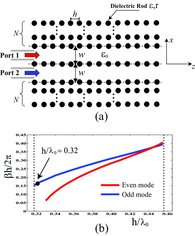
The two coupled symmetric pillar type PCWs consisting of square lattice of dielectric rods in free space is illustrated in Fig. 1a. The guiding regions are bounded by the upper and lower photonic crystals, which have a common period along the -axis. The parameters of the structure are chosen as , , and where and are the relative permittivity and radius of the dielectric circular rods, is a width of the PCW and is the number of layers of the upper and lower photonic crystals. The length of the photonic crystals is . In the case of pillar type photonic crystal waveguide, the modes are confined in the guiding region only due to the existence of bandgap region, since the effective index of the guiding region is smaller than that of the cladding region. Under the adjusted parameters, the pillar type photonic crystal has a photonic bandgap for -polarized field in the frequency range , where is a wavelength in a free space. The dispersion diagrams of the coupled PCWs (Fig. 1) are studied based on the coupled-mode formulation [8, 9], which we have recently proposed using the first-order perturbation theory taking into account a weak coupling effect. Based on the derived coupled-mode equations [8, 9] normalized propagation constant of the pillar type coupled PCWs (Fig.1) for the even mode and odd mode versus the normalized frequency is calculated and it is plotted in Fig. 1b by red line and blue lines, respectively. It should be noted that no other propagating modes exist in the frequency range . From the figure it follows that in the lower frequency region the even mode enters in a cutoff region and only odd mode is propagating along the -axis. From a viewpoint of the practical application of the coupled PCWs structure as all-optical amplifier, we are interested in the frequency region , where only one propagating mode exists. All the numerical analysis that follow are conducted at the fixed normalized frequency .
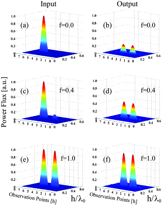
To validate the use of the coupled PCWs as all-optical amplifier, firstly, we analyze the power flux of a continuous signal launched into the coupled PCWs (Fig.1) using the FDTD method [10, 11]. We have chosen the discretization step size as , where is the lattice period. The discretized time step is , by which the stability condition of FDTD method is satisfied. The analysis region is surrounded by Berenger’s PML with thickness of 20 cells in all of the surrounding walls. The initial excitations are injected into the coupled PCWs at through Port 1 and Port 2. Input Ports are bounded by PEC walls marked by gray lines in Fig. 1. The output signal is registered by the detector placed at a distance inside the coupled PCWs. The length of the detector is and it is parallel along the -axis. To demonstrate the effect of all-optical amplification, firstly we inject a signal with unit amplitude in Port 1, whereas no signal is launched in Port 2. The power flux of the total input signal is illustrated in Fig. 2a. In this case the total input could be represented as a sum of even and odd modes and since the coupled PCWs support only the odd mode at (Fig. 1b), the even mode is completely reflected and the total output power is half of the input power as shown in Fig. 2b. Next, we inject a continuous signal in Port 2 with an amplitude . The total input power flux is illustrated in Fig. 2c. It is important to mention that in order to guide an input signal into the coupled PCWs, which supports only one odd mode, the injected signals in Port 1 and Port 2 should be with opposite phases. The output power flux is presented in Fig. 2d. The amplification coefficient is calculated as
| (1) |
and it is equal to . It is worth mentioning that in case of weakly coupled PCWs the result for the amplification coefficient is very close to the result obtained using the rigorous theoretical analysis [7]
| (2) |
Additionally, our numerical analysis have vividly demonstrated that the amplification coefficient is substantially improved in comparison to the results for the conventional dielectric waveguides separated by silver metallic film [7]. It is obvious that an increase of the amplification coefficient is caused by the absence of energy losses in pillar type coupled PCWs. Finally, we further increase the amplitude of the injected signal in input Port 2 up to and the power flux of the input and output signals are illustrated in Fig. 2e and Fig. 2f, respectively. The amplification coefficient is . The results for the amplification coefficients at different amplitudes are presented in some detail in Table 1. From the results it follows that the amplification coefficient is inversely proportional to the amplitude of the input signal.

Next, in Fig. 3 we are analyzing the near field distributions of the Gaussian pulse propagating in the weakly coupled PCWs. The time waveform of the Gaussian pulse is centered at the time step 4500 and the full width at half maximum (FWHM) of the pulse is 1500 time steps. Near field distributions at , and at different moments of time are presented in Fig. 3a - Fig. 3f, respectively. The amplification coefficient of Gaussian pulse is calculated and the results are presented in Table 1. Similarly to the previous case of continuous signal, a good agreement between our results and the case considered in [7]. In comparison, the near field distribution of the Gaussian pulse injected in Port 1 and Port 2 with the same phase (even mode) is illustrated in Fig. 3g. The pulse in completely reflected from the coupled PCWs and there is no power carried inside the coupled PCWs. This is due to the fact that the coupled pillar type PCWs do not support the even mode at the normalized frequency (Fig. 1b). The coupled PCWs behave as a phase filter providing maximum output power for the signals with the opposite phases (Fig. 3a - Fig. 3f) and zero power for the signal with the same phases (see Fig. 3g).
| Continuous | Gaussian | Rigorous Analysis [7] | |
| Signal | Pulse | ||
| 0.2 | 5.30 | 4.90 | 5.50 |
| 0.4 | 2.82 | 2.70 | 3.00 |
| 0.5 | 2.38 | 2.29 | 2.50 |
| 0.8 | 1.68 | 1.62 | 1.75 |
| 1.0 | 1.45 | 1.41 | 1.50 |
III Conclusion
In this manuscript, for the first time, we have proposed a weakly coupled photonic crystals waveguide as a realistic model for all-optical amplifier. It should be noted that the amplification effect of the optical signal proposed in the manuscript is quite different from that in homodyne receiver scheme, where the signal intensity is amplified at the receiving area only, whereas the total signal is not amplified. The authors believe that one of the promising practical applications of the proposed structure could be optical transistors. Being able to precisely control the intensity of one light beam using another could be crucial to the development of optical transistors capable of performing complex light-controlling in all-optical circuits.
References
- [1] E. Yablonovitch, ”Inhibited spontaneous emission in solid-state physics and electronics,” Phys. Rev. Lett., vol. 58, pp. 2059-2062, 1987.
- [2] S. John, ”Strong localization of photons in certain disordered dielectric superlattices,” Phys. Rev. Lett., vol. 58, pp. 2486-2489, 1987.
- [3] A. Adibi, Y. Xu, R. Lee, A. Yariv and A. Scherer, ”Properties of the slab modes in photonic crystal optical waveguides,” J. Lightwave Technology, vol. 18, pp. 1554-1564, 2000.
- [4] A. Scherer, T. Doll, E. Yablonovitch, H.O. Everitt, and J.A. Higgins, ”Special Section on Electromagnetic Crystal Structures, Design, Synthesis, and Applications,” J. Lightwave Technol., vol. 17, pp. 1928-2207, 1999.
- [5] E. Yablonovitch, ”Photonic band-gap structures,” J. Opt. Soc. Am. B, vol. 10, pp. 283-295, 1993.
- [6] M. Izutsu, Y. Nakai, T. Sueta, ”Operational mechanism of the single mode optical waveguide Y junction”, Opt. Lett., vol. 7, pp. 136-138, 1982.
- [7] R. Khomeriki and J. Leon, ”All-optical amplification in metallic subwavelength waveguides,” Physical Review A, vol. 87, pp. 053806, 2013.
- [8] K. Yasumoto, V. Jandieri and Y. Liu, ”Coupled-Mode Formulation of Two-Parallel Photonic Crystal Waveguides,” Journal of the Optical Society of America A, vol. 30, pp. 96-101, 2013.
- [9] V. Jandieri, K. Yasumoto and J. Pistora, ”Coupled-Mode Analysis of Contra-Directional Coupling between Two Asymmetric Photonic Crystals Waveguides”, Journal of the Optical Society of America A, vol. 31, pp. 518-523, 2014.
- [10] A. Taflove, Computational Electrodynamics: The Finite-Difference Time-Domain Method, Artech House, Norwood, 1995.
- [11] M. Qiu, K. Azizi, A. Karlsson, M. Swillo and B. Jaskorzynska, ”Numerical studies of mode gaps and coupling efficiency for line-defect waveguides in two-dimensional photonic crystals,” Physical Review B, vol. 64, pp. 155113, 2001.