Single Spin Optically Detected Magnetic Resonance with E-Band Microwave Resonators.
Abstract
Magnetic resonance with ensembles of electron spins is nowadays performed in frequency ranges up to GHz and in corresponding magnetic fields of up to T. However, experiments with single electron and nuclear spins so far only reach into frequency ranges of several GHz, where existing coplanar waveguide structures for microwave (MW) delivery are compatible with single spin readout techniques (e.g. electrical or optical readout). Here, we explore the frequency range up to GHz, respectively magnetic fields of up to T for single spin magnetic resonance in conjunction with optical spin readout. To this end, we develop MW resonators with optical single spin access. In our case, rectangular E-band waveguides guarantee low-loss supply of microwaves to the resonators. Three dimensional cavities, as well as coplanar waveguide resonators enhance MW fields by spatial and spectral confinement with a MW efficiency of . We utilize single NV centers as hosts for optically accessible spins, and show, that their properties regarding optical spin readout known from smaller fields (T) are retained up to fields of T. In addition, we demonstrate coherent control of single nuclear spins under these conditions. Furthermore, our results extend the applicable magnetic field range of a single spin magnetic field sensor. Regarding spin based quantum registers, high fields lead to a purer product basis of electron and nuclear spins, which promises improved spin lifetimes. For example, during continuous single-shot readout the 14N nuclear spin shows second-long longitudinal relaxation times.
pacs:
I Introduction
Single electron and nuclear spin magnetic resonance is routinely detected on a variety of systems nowadays, ranging from single moleculesWrachtrup et al. (1993a, b), solid state defectsJelezko et al. (2004); Weber et al. (2011); Pla et al. (2013) to rare earth ionsSiyushev et al. (2014).
In all these cases, spin control is performed via oscillating magnetic fields, but readout is performed either electrically or optically.
For small magnetic fields and hence moderate microwave (MW) frequencies up to several GHz, this is compatible with wires, antennas and coplanar waveguide (CPW) structures manufactured close to the spin Toyli et al. (2010); Pla et al. (2013).
At higher MW frequencies the transmission-loss of coaxial cables increases drastically.
The main reason is the decreasing skin depth 1/, which leads to higher effective resistivity in the conductor line.
Increasing the diameter of the coaxial cables to compensate this effect is only possible up to a certain point, since it decreases the moding-frequency.
Additionally, at higher frequencies (e.g. in the E-band from GHz to GHz) semiconductor-based MW sources and amplifiers currently achieve an output power of less than dBm.
Taking this into account, novel strategies for combining single spin magnetic resonance at high frequencies and specific readout techniques need to be developed that ensure a high microwave-power-to-magnetic-field conversion efficiency (respectively microwave-power-to-Rabi-frequency conversion efficiency ).
Working in the E band extends the accessible range of single spins as magnetic field sensors up to T.
Furthermore, experiments at such high bias magnetic field promise additional striking improvements.
For spin based quantum information candidate systems like phosphorous in silicon (Si:P)Pla et al. (2013); Morello et al. (2010), rare-earth ionsSiyushev et al. (2014); Kolesov et al. (2013, 2012); Yin et al. (2013) or nitrogen-vacancy (NV) centers in diamondWaldherr et al. (2014); Dolde et al. (2014); Togan et al. (2010); Bernien et al. (2013) higher fields reduce dressing among electron and nuclear spin states.
Hence, energy eigenstates converge to pure product spin states, which promises improved coherence properties and nuclear spin accessMcCamey et al. (2010); Waldherr et al. (2014).
The single spin sensors (e.g. NV centers in diamondBalasubramanian et al. (2008); Maze et al. (2008)) can be applied for nanoscale detection of external electron and nuclear spinsHäberle et al. (2015); Mamin et al. (2013); DeVience et al. (2015); Staudacher et al. (2013); Grotz et al. (2011); Grinolds et al. (2013).
High fields are particularly important for nuclear spin detection because under these conditions chemical shifts of nuclear spin resonances allow chemically specific sensing in homonuclear environments.
Finally, the thermal spin polarization increases with higher available magnetic fields.
Here, we develop and demonstrate a single spin magnetic resonance setup with optical spin readout (optically detected magnetic resonance – ODMR) for magnetic fields up to T.
This method is in principle also applicable to higher magnetic fields.
As a single spin test system we use nitrogen-vacancy (NV) color centers in diamondGruber et al. (1997).
The electron spin of the NV center is a triplet () with a zero field splitting of GHz.
An external magnetic field aligned along the NV axis lifts the degeneracy of the energy levels.
The latter spin states split with .
Single NV centers are optically addressed via confocal microscopy, and MW fields in the E-band are delivered via respective rectangular waveguides (WR-12).
At the position of the NV center, we fabricate waveguide and CPW resonators for spatial and spectral field concentration.
Single nuclear spins are controlled via radio-frequency (RF) fields delivered by wires and read out by electron nuclear double resonance (ENDOR) via the NV center electron spin.
II single spin ODMR setup up to 3T
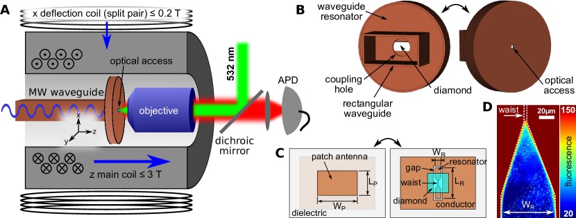
At the heart of our single spin ODMR setup there is the confocal microscope which focuses nm excitation laser light through an oil immersion objective onto an NV center in diamond (see figure 1).
The red-shifted fluorescence response is spectrally and spatially filtered and finally imaged onto a single photon counting module.
We utilize a home-built microscope which fits in the room temperature bore (diameter cm) of a superconducting magnet with up to T main field and up to T perpendicular deflection coils (Scientific Magnetics).
We have placed sample positioners and the objective into the bore, all other optical, MW and RF elements are placed outside the magnet.
The main magnetic field axis coincides with the optical axis, optimizing the setup for (111)-oriented diamond substrates with NV centers pointing along the surface normal.
For this work a (111) diamond plate was cut from a low-strain type-IIa high-pressure-high-temperature (HPHT) crystal with an average substitutional nitrogen concentration of ppb and natural abundance of 13C.
The plate was irradiated with MeV electrons to a total dose of and was subsequently annealed at C for 2 hours in vacuum.
Then, a thin film of m was obtained by laser-cutting and polishing from the plate.
For the generation of MW we combine an Anritsu signal generator MG3690C with an OML S12MS frequency multiplier (6x) system with a measured output power of dBm.
In the frequency range from GHz to GHz we employ a MW power amplifier (Sage Millimeter Inc.) with an output power of dBm (P-1dB).
Microwaves in the E band are guided to the NV center via a rectangular waveguide (WR-12).
At the end of the waveguide we concentrate the microwave radiation spectrally and spatially to a region of diamond containing NV centers.
We have implemented two different approaches for microwave delivery into the diamond: A three dimensional waveguide cavity and a transition from rectangular waveguide to CPW resonator (see figure 1).
As a first approach, we use a circular TM110 cavity attached to the rectangular waveguide as depicted in figure 1B.
The diamond is placed inside this resonator on the face opposite to the coupling hole.
The latter opposite metal face has a hole for optical access.
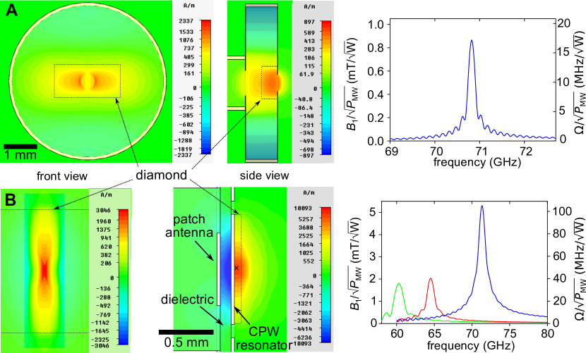
Inside the cavity a MW field builds up, which is perpendicular to the bias field and leads to a Rabi frequency of the NV electron spin of , with the NV electron g-factor and the Bohr magneton .
The tailored transition from waveguide to CPW resonator (see figure 1C) was inspired by low-loss microstrip line to waveguide transitions in automotive radar systemsIizuka et al. (2002).
In contrast, our goal is to concentrate the MW field at the end of the waveguide.
To this end we design an assembly containing a tapered dipole antenna (GHz).
Close to the waist position, MW radiation is spectrally and spatially confined and electron spins can be coherently manipulated.
Optical access is possible above the CPW resonator or inside the gaps.
In addition to high MW efficiencies, both mentioned approaches should provide a linewidth of MHz.
This allows addressing proximal nuclear spins with hyperfine couplings up to MHzMizuochi et al. (2009).
In addition, fast gate operation times are not limited by a narrow resonator linewidth.
RF is supplied by a wire across the CPW resonator perpendicular to the dipole axis to reduce losses (see figure 4B).
III Microwave resonators — design and simulations
III.1 TM110 waveguide cavity
The first approach to increase the MW field at the NV center location is a waveguide cavity with a suitable mode.
For the selection of the cavity mode, the orientation of the external magnetic field and the optical axis play an important role.
The latter rules out TE011 mode resonators often used in EPR because of the inappropriate field profile,which is concentrated in the center of the cylindrical MW cavity where, consequently, the sample has to be mounted.
Our microscope objective has a working distance of mm.
Contrary to this, a typical TE011 cavity working at GHz has a radius of mm and length of mm making an optical access unfeasiblePozar (2004).
Our cavity mode of choice is the TM110 mode.
In the proper configuration, its concentrated field has an orientation perpendicular to one of the crystallographic NV orientations in a diamond with (111) surface.
Inductive coupling from the WR-12 waveguide to the cavity is accomplished by a centered hole on the circular surface of the cavity facing the waveguide.
The orientation of the incoming field from the waveguide matches the orientation of the field of one out of two nominally degenerate TM110 modes in the cavity with perpendicular polarizations, (see figure 2) resulting in efficient couplingPozar (2004).
is maximum in the center of the cavity and in transverse direction to the bias magnetic field (see figure 2A).
The field has no node in longitudinal direction.
Hence, a centered hole in the second circular surface provides an optical access to the area with a highly concentrated field.
In addition, the higher refractive index of diamond compared to air leads to a further field enhancement in the diamond.
The cavity frequency is defined by the radius of the cavity.
Decreasing the cavity length has no effect on the resonance frequency, but increases the ratio of quality factor and cavity volume Pozar (2004).
This ratio is approximately doubled for compared to the case of , resulting in a higher field strength.
By varying the diameter of the coupling hole, one can tune the regime between an undercoupled, a critically coupled and an overcoupled cavity.
In our case, a critically coupled cavity results in maximum at the NV center location.
Simulations were performed in order to estimate the optimum coupling hole diameter, predicting a cavity quality factor of .
m below the optical access a maximum MW efficiency of () is expected.
The TM110 cavity is assembled out of three separate parts.
The main component is a copper plate with a round bore and a thickness of mm.
The second part is a copper film with a hole for inductive coupling to the cavity.
The cavity is closed on the other side by a glass slide with a thin copper layer comprising a hole for optical access (m diameter).
All parameters of the cavity are listed in table 1.
One of the loss channels is conductive loss.
There is a non-zero current density across the contact area between the circular surfaces and the cylindrical part, leading to conductive losses at the edges of the cavity due to non-ideal contacts.
Furthermore, surface roughness is a crucial point which is improved by polishing the copper plate.
Radiative losses also have to be considered.
Because the optical access in our case is almost as large as the hole for inductive coupling, the accompanied radiative loss is not negligible.
Moreover, a large optical access decreases the field in the region of interest (see the xy plot of the field in figure 2A).
In fact, the MW efficiency increases to () at the aforementioned position by removing the optical access in the simulation.
In principle, other cavity modes can be used as well.
In the case of the TM010, the field is maximum at the edges of the cavity where both the optical microscopy and the MW coupling from the waveguide would have to be placedPozar (2004).
Another possibility is to shape the diamond itself, according to the corresponding cavity parameters, and cover it with metal.
In this case, the conductive losses at the edges and the mode volume would be decreased.
The metal layer where the diamond is attached to has a thickness of m, which is above the skin depth of the applied MW radiation (GHz), but in the range of the skin depth (m) for nuclear spin resonance frequencies of MHz.
Hence, a wire outside of the resonator can be used to deliver RF for coherent nuclear spin control for a proper metal layer thickness.
| TM110 cavity | ||
|---|---|---|
| diameter | mm | |
| length | mm | |
| diameter of optical access | m | |
| diameter of MW coupling hole | m | |
| thickness of metal face with optical access | m | |
| thickness of metal face with MW coupling hole | m | |
| material | copper | |
| Waveguide to CPW resonator | #1 | #2 |
| patch antenna length | m | m |
| patch antenna width | m | m |
| resonator length | m | m |
| resonator width | m | m |
| relative dielectric constant | 2.9 | |
| dielectric thickness | m | |
| conductor thickness | m | m |
| gap CPW | m | m |
| width of waist | m | m |
| length of waist | m | m |
| conductor material | copper | |
| dielectric material | Rogers Ultralam 3850 | |
III.2 Waveguide to coplanar resonator transition
Further enhancement of the RF magnetic field amplitude can be achieved by an additional confinement in the spatial domain.
To this end we design an assembly of a tapered /2 CPW resonator and a patch antenna separated by a dielectric (see figure 1C and figure 2B).
The patch antenna is facing the rectangular waveguide.
The whole assembly is coupled capacitively to the TE10 mode of the rectangular waveguide.
The resonant mode of the assembly in which we are interested can be described as follows.
The tapered resonator part is excited strongly, with mirror charges and corresponding current densities forming on the patch antenna.
Additional oscillating current densities are forming in the part of the ground plane surrounding the tapered resonator.
Consequently, the field is mainly concentrated inside the dielectric and oriented perpendicular to both the bias field and the axis of the tapered resonator.
A considerable field also exists outside the dielectric above the center region of the tapered resonator.
Hence, the perfect position for an NV center is inside the dielectric, which would then be the diamond itself.
Another alternative is placing a diamond on top of the resonator and using an NV center close to the center of the tapered resonator.
Because of the commercial availability of dielectric media, the thickness was fixed to m in our experiment.
We do not have sufficiently large diamond samples to use diamond as the dielectric material.
The strength of the field inside the dielectric would increase for a thinner material.
However, critical coupling to the rectangular waveguide can be achieved in any case by adjusting geometric parameters of the CPW resonator (see table 1).
By narrowing the CPW resonator in the center, the current density and, accordingly, the field strength close to the waist are enhanced (see figure 2B).
We have simulated and produced two CPW resonators with mainly two different widths of the waist (see table 1).
For a resonator tapered to a waist of m width (resonator #2),
the simulated MW efficiency m above the resonator amounts to ().
The ground plane around the resonator reduces radiative losses and the patch antenna leads to a concentration of MW energy inside the resonator assembly.
Dielectric materials between CPW resonator and patch antenna with low loss and high dielectric constant can mitigate effects of dielectrics outside of the resonator assembly.
Apart from losses, dielectrics such as diamond or immersion oil on the resonator assembly also lead to a shift of the resonance (see figure 3D).
Conductive losses can be reduced by smooth metal surfaces.
For CPW resonator #2 we have simulated a quality factor of , where the contributions of conductive, dielectric and radiative losses are estimated to be 192, 891 and 204, respectively.
We have to consider additional resonances of the whole assembly, due to similar length scales for all coupled parts.
In fact, the patch antenna utilized for improved field concentration can have a resonance close to that of the dipole antenna.
For improper dimensions of the assembly the patch antenna almost completely cancels the transverse field above and below the CPW resonator.
In addition to electron spin manipulation by the CPW resonator, a wire or a coil can deliver radio frequencies in order to excite nuclear spin transitions (see figure 4B).
The CPW resonators were fabricated out of double sided printed circuit boards (Rogers Ultralam 3850, see table 1) by optical lithography and wet chemical etching.
IV Results and Discussion
IV.1 Single spin optically detected magnetic resonance
The introduced MW resonators enabled the implementation of single spin ODMR at high magnetic fields.
The basic sequence for a typical pulsed ODMR measurement consists of a spin state reading and polarizing laser pulse accompanied by fluorescence detection, followed by a MW pulse (compare figure 4C).
This basic sequence is continuously applied Steiner et al. (2010).
If the MW frequency corresponds to the spin transition frequency, less fluorescence is emitted.
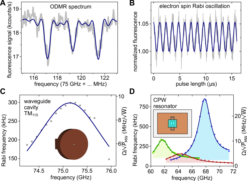
In figure 3A, an ODMR spectrum of the to transition is visible.
Due to the hyperfine interaction with the NV center’s 14N nuclear spin, the transition is split into three distinctive features.
The applied magnetic field is about T.
Varying the length of the microwave pulse results in coherent oscillations of the spin projection in z direction (see figure 3B).
Since the frequency of MW induced Rabi oscillations is proportional to , measuring it as a function of the microwave transition frequency (and thus the external magnetic field) provides information about the performance of the microwave assembly.
The results for the circular waveguide cavity (TM110 mode) can be seen in figure 3B.
The NV center was located in the center of the optical hole and m deep in the diamond.
The measured quality factor is .
For a maximum Rabi frequency of kHz, the MW efficiency is .
This factor is well below the theoretically predicted one.
In the simulations, the conductive loss caused by the imperfect connection between the cavity element and the metal termination plates was neglected.
Moreover, the surface roughness of the copper film containing the coupling hole can be improved.
As discussed above, a cavity made out of polished diamond would mitigate these loss mechanisms and enhance the concentration of the MW field because of a smaller mode volume.
In the experiment, the diameter of the optical hole was m to ensure a large area of detectable NVs.
This can be scaled down in order to reduce the radiative losses.
We have produced two CPW resonators mainly differing by the width (see table 1) of their waists while all other parameters where optimized for strongest field m above the waist.
The parameters given in the table have been confirmed by optical microscopy.
CPW resonator #1 has a large waist of m compared to resonator #2 with a waist of m.
Hence, resonator #2 is expected to show a larger field close to the waist.
The resonance curves in figure 3D were again recorded by measuring field (and therefore MW frequency) dependent Rabi oscillations.
The different colors correspond to different configurations of diamond and resonators.
The green and the red curves are measured using resonator #1.
In the case of the green curve, the mm diamond is fully covering the CPW resonator while in the case of the red plot the diamond was covering half of the resonator.
We attribute the GHz shift of the resonance frequency to the influence of the diamond and its large dielectric constant as is predicted by the simulation results (see figure 2B).
The differences in amplitude are mainly due to different distances of the measured NVs to the waist of the resonator.
The maximum MW efficiency measured for this resonator is (green curve) for an NV center m above the waist.
The blue curve belongs to resonator #2 with the diamond centered on the resonator.
The MW efficiency reaches for an NV center m above the resonator close to the waist where the tapering has a width of m.
At the position of the waist (with potentially even higher MW efficiency) high background fluorescence from the dielectric material prevented ODMR measurements.
In conclusion, decreasing the waist leads to a further spatial concentration and thus enhancement of the field.
The quality factors of CPW resonators #1 and #2 are and respectively, whereas the waveguide cavity reaches .
Both waveguide cavity and CPW resonator are useful for our experiments.
Their linewidths respectively quality factors, however, can still be improved.
The advantage of the CPW resonator approach is the concurrent spectral and spatial confinement yielding higher MW efficiencies.
IV.2 Quantum nondemolition measurements and coherent manipulation of single nuclear spin
As explained in the introduction, one of the main reasons to investigate the behavior of NV centers in high magnetic field is the control of surrounding nuclear spins.
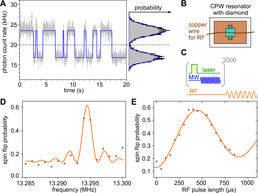
Readout of these proximal spins is facilitated by mapping the population onto the NV electron spin by applying a -gate, and consecutive electron spin readout Neumann et al. (2010).
The CNOT-gate is implemented by a nuclear spin state selective electron -pulse (see figure 4C).
In order to be able to read out the nuclear spin state in a single shot, this measurement has to be repeated on the order of 1000 times, without the nuclear spin to flip.
As has been shown previously, the main source of longitudinal relaxation for the nitrogen nuclear spin are flip-flop events with the corresponding electron spin.
The probability for this to occur can be reduced quadratically with the applied magnetic field.
Exemplary continuous single shot measurements of the 14N nuclear spin state can be seen in figure 4A.
The measurement sequence is the same as for pulsed ODMR, but with a fixed microwave frequency.
The fluorescence timetrace reveals quantum jumps between two distinct levels, corresponding to different nuclear spin states (depicted by the blue state trace).
On the right side, a histogram of the fluorescence timetrace shows two separable poissonian distributions (the blue line depicts a fit of the superposition of two poissonians).
This enables single shot readout, as well as initialization by measurement of the nitrogen nuclear spin.
The fluorescence timetrace shows longitudinal relaxation times of the 14N nuclear spin on the order of seconds (see figure 4A) during continuous projective measurements, an improvement of one order compared to previous measurements performed at T Neumann et al. (2010).
To demonstrate coherent control of the nuclear spin, the NMR spectrum and Rabi oscillations are measured.
A m wire is placed across the diamond surface and connected to a RF source to enable nuclear spin manipulation at transition frequencies of several MHz (see figure 4B).
The nuclear spin measurements follow a common approach:
The nuclear spin is measured two times in a single shot, both measurements are then correlated to see if a spin flip occurred.
This probability is measured for different kinds of spin manipulation in between the two nuclear spin state measurements.
By sweeping the frequency of the applied microwave, an NMR spectrum can be recorded (see figure 4D).
Varying the microwave pulse length at the resonant frequency leads to coherent Rabi oscillations (see figure 4E).
IV.3 Conclusion
In this study, electron spin resonance and optical microscopy in the E-band is shown to be feasible by exploiting MW resonators.
Spectral confinement is utilized in the cylindrical MW cavity approach.
The waveguide to tapered CPW resonator allows additional confinement in the spatial domain.
A high MW efficiency of () enables ODMR measurements even with a low-power MW source.
At a magnetic field of T single-shot readout of single nuclear spin reveals seconds-long longitudinal relaxation times.
In addition to readout, coherent control of the nuclear spin via an additional copper wire is shown.
In principle the presented CPW resonator approach is extendable to even higher frequencies and corresponding magnetic fields.
Then as well as in the current frequency range, free space optics might be used for focusing millimeter waves onto a suitable antenna assembly incorporating single optically addressable spins.
While preparing the manuscript we became aware of a demonstration of ODMR of single electron spins at T Stepanov et al. (2015) where our approach might also lead to improvements.
Acknowledgements.
We thank A. Denisenko, A. Momenzadeh and F. Fávaro de Oliveira for sample preparation. Furthermore, we thank G. Untereiner for TM cavity production. We acknowledge financial support by the German Science Foundation (SFB-TR 21, SPP1601), the EU (SIQS) and the JST.References
- Wrachtrup et al. (1993a) J. Wrachtrup, C. von Borczyskowski, J. Bernard, M. Orritt, and R. Brown, Nature 363, 244 (1993a).
- Wrachtrup et al. (1993b) J. Wrachtrup, C. von Borczyskowski, J. Bernard, M. Orrit, and R. Brown, Physical Review Letters 71, 3565 (1993b).
- Jelezko et al. (2004) F. Jelezko, T. Gaebel, I. Popa, M. Domhan, A. Gruber, and J. Wrachtrup, Physical Review Letters 93, 130501 (2004).
- Weber et al. (2011) J. R. Weber, W. F. Koehl, J. B. Varley, A. Janotti, B. B. Buckley, C. G. V. d. Walle, and D. D. Awschalom, Applied Physics Letters 109, 102417 (2011).
- Pla et al. (2013) J. J. Pla, K. Y. Tan, J. P. Dehollain, W. H. Lim, J. J. L. Morton, F. A. Zwanenburg, D. N. Jamieson, A. S. Dzurak, and A. Morello, Nature 496, 334 (2013).
- Siyushev et al. (2014) P. Siyushev, K. Xia, R. Reuter, M. Jamali, N. Zhao, N. Yang, C. Duan, N. Kukharchyk, A. D. Wieck, R. Kolesov, and J. Wrachtrup, Nature Communications 5 (2014), 10.1038/ncomms4895, arXiv:1405.5258 [cond-mat, physics:quant-ph].
- Toyli et al. (2010) D. M. Toyli, C. D. Weis, G. D. Fuchs, T. Schenkel, and D. D. Awschalom, Nano Letters 10, 3168 (2010).
- Morello et al. (2010) A. Morello, J. J. Pla, F. A. Zwanenburg, K. W. Chan, K. Y. Tan, H. Huebl, M. Mottonen, C. D. Nugroho, C. Yang, J. A. van Donkelaar, A. D. C. Alves, D. N. Jamieson, C. C. Escott, L. C. L. Hollenberg, R. G. Clark, and A. S. Dzurak, Nature 467, 687 (2010).
- Kolesov et al. (2013) R. Kolesov, K. Xia, R. Reuter, M. Jamali, R. Stöhr, T. Inal, P. Siyushev, and J. Wrachtrup, Physical Review Letters 111, 120502 (2013).
- Kolesov et al. (2012) R. Kolesov, K. Xia, R. Reuter, R. Stöhr, A. Zappe, J. Meijer, P. R. Hemmer, and J. Wrachtrup, Nature Communications 3, 1029 (2012).
- Yin et al. (2013) C. Yin, M. Rancic, G. G. de Boo, N. Stavrias, J. C. McCallum, M. J. Sellars, and S. Rogge, Nature 497, 91 (2013).
- Waldherr et al. (2014) G. Waldherr, Y. Wang, S. Zaiser, M. Jamali, T. Schulte-Herbrüggen, H. Abe, T. Ohshima, J. Isoya, J. F. Du, P. Neumann, and J. Wrachtrup, Nature 506, 204 (2014).
- Dolde et al. (2014) F. Dolde, V. Bergholm, Y. Wang, I. Jakobi, B. Naydenov, S. Pezzagna, J. Meijer, F. Jelezko, P. Neumann, T. Schulte-Herbrüggen, J. Biamonte, and J. Wrachtrup, Nature Communications 5, 3371 (2014).
- Togan et al. (2010) E. Togan, Y. Chu, A. S. Trifonov, L. Jiang, J. Maze, L. Childress, M. V. G. Dutt, A. S. Sørensen, P. R. Hemmer, A. S. Zibrov, and M. D. Lukin, Nature 466, 730 (2010).
- Bernien et al. (2013) H. Bernien, B. Hensen, W. Pfaff, G. Koolstra, M. S. Blok, L. Robledo, T. H. Taminiau, M. Markham, D. J. Twitchen, L. Childress, and R. Hanson, Nature 497, 86 (2013).
- McCamey et al. (2010) D. R. McCamey, J. V. Tol, G. W. Morley, and C. Boehme, Science 330, 1652 (2010).
- Balasubramanian et al. (2008) G. Balasubramanian, I. Y. Chan, R. Kolesov, M. Al-Hmoud, J. Tisler, C. Shin, C. Kim, A. Wojcik, P. R. Hemmer, A. Krueger, T. Hanke, A. Leitenstorfer, R. Bratschitsch, F. Jelezko, and J. Wrachtrup, Nature 455, 648 (2008).
- Maze et al. (2008) J. R. Maze, P. L. Stanwix, J. S. Hodges, S. Hong, J. M. Taylor, P. Cappellaro, L. Jiang, M. V. G. Dutt, E. Togan, A. S. Zibrov, A. Yacoby, R. L. Walsworth, and M. D. Lukin, Nature 455, 644 (2008).
- Häberle et al. (2015) T. Häberle, D. Schmid-Lorch, F. Reinhard, and J. Wrachtrup, Nature Nanotechnology 10, 125 (2015).
- Mamin et al. (2013) H. J. Mamin, M. Kim, M. H. Sherwood, C. T. Rettner, K. Ohno, D. D. Awschalom, and D. Rugar, Science 339, 557 (2013).
- DeVience et al. (2015) S. J. DeVience, L. M. Pham, I. Lovchinsky, A. O. Sushkov, N. Bar-Gill, C. Belthangady, F. Casola, M. Corbett, H. Zhang, M. Lukin, H. Park, A. Yacoby, and R. L. Walsworth, Nature Nanotechnology 10, 129 (2015).
- Staudacher et al. (2013) T. Staudacher, F. Shi, S. Pezzagna, J. Meijer, J. Du, C. A. Meriles, F. Reinhard, and J. Wrachtrup, Science 339, 561 (2013).
- Grotz et al. (2011) B. Grotz, J. Beck, P. Neumann, B. Naydenov, R. Reuter, F. Reinhard, F. Jelezko, J. Wrachtrup, D. Schweinfurth, B. Sarkar, and P. Hemmer, New Journal of Physics 13, 055004 (2011).
- Grinolds et al. (2013) M. S. Grinolds, S. Hong, P. Maletinsky, L. Luan, M. D. Lukin, R. L. Walsworth, and A. Yacoby, Nature Physics 9, 215 (2013).
- Gruber et al. (1997) A. Gruber, A. Drabenstedt, C. Tietz, L. Fleury, J. Wrachtrup, and C. vonBorczyskowski, Science 276, 2012 (1997).
- Iizuka et al. (2002) H. Iizuka, T. Watanabe, K. Sato, and K. Nishikawa, IEICE TRANSACTIONS on Communications E85-B, 1169 (2002).
- Mizuochi et al. (2009) N. Mizuochi, P. Neumann, F. Rempp, J. Beck, V. Jacques, P. Siyushev, K. Nakamura, D. Twitchen, H. Watanabe, S. Yamasaki, F. Jelezko, and J. Wrachtrup, Physical Review B 80, 041201 (2009).
- Pozar (2004) D. Pozar, Microwave Engineering (Wiley, 2004).
- Steiner et al. (2010) M. Steiner, P. Neumann, J. Beck, F. Jelezko, and J. Wrachtrup, Physical Review B 81, 035205 (2010).
- Neumann et al. (2010) P. Neumann, J. Beck, M. Steiner, F. Rempp, H. Fedder, P. R. Hemmer, J. Wrachtrup, and F. Jelezko, Science 329, 542 (2010).
- Stepanov et al. (2015) V. Stepanov, F. H. Cho, C. Abeywardana, and S. Takahashi, Applied Physics Letters 106, 063111 (2015).