Antenna-coupled photon emission from hexagonal boron nitride tunnel junctions
Abstract
The ultrafast conversion of electrical signals to optical signals at the nanoscale is of fundamental interest for data processing, telecommunication and optical interconnects. However, the modulation bandwidths of semiconductor light-emitting diodes are limited by the spontaneous recombination rate of electron-hole pairs, and the footprint of electrically driven ultrafast lasers is too large for practical on-chip integration. A metal-insulator-metal tunnel junction approaches the ultimate size limit of electronic devices and its operating speed is fundamentally limited only by the tunneling time. Here, we study the conversion of electrons – localized in vertical gold-hexagonal boron nitride-gold tunnel junctions – to free-space photons, mediated by resonant slot antennas. Optical antennas efficiently bridge the size mismatch between nanoscale volumes and far-field radiation and strongly enhance the electron-photon conversion efficiency. We achieve polarized, directional and resonantly enhanced light emission from inelastic electron tunneling and establish a novel platform for studying the interaction of electrons with strongly localized electromagnetic fields.
Optical nanoantennas are elements that couple free space radiation to material structures with length scales that are orders of magnitude smaller than the wavelength of a visible photon (400 to 700 nm) bharadwaj09a ; alu08a ; greffet10a ; novotny11a ; biagioni12a .
Incoming radiation is converted into localized surface plasmon polaritons (LSPPs) – time-harmonic oscillations of the free electron gas
– that concentrate electromagnetic energy into ultrasmall volumes schuller10 . Many optical antennas owe their design to their macroscopic radiofrequency predecessors like linear dipole antennas muehlschlegel05 ; alu08a , Yagi-Uda antennas curto10
or bow-tie antennas kinkhabwala09 .
Classical antennas are used to generate radiofrequency (RF) waves by driving them at the respective frequency electrically or – in reverse – to generate RF electrical signals from incoming electromagnetic radiation. Optical antennas on the other hand have been mostly operated on a “light-in / light-out” basis novotny11a . This paradigm has recently started to shift towards the integration of optical antennas in optoelectronic devices for photovoltaics atwater10 , photon detection tang08 ; knight11 and
surface plasmon excitation huang14 . Here we report on the realization of ultrafast solid-state light-emitting tunnel devices based on arrays of electrically driven optical antennas.
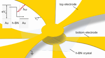
Applying a voltage to a metal-insulator-metal junction yields a current due to electrons tunneling through the insulator from occupied states in one electrode to unoccupied states in the other electrode. The majority of electrons tunnel elastically, maintaining their energy during the tunneling process. The excess energy of the “hot electron” is subsequently thermalized. In 1976, Lambe and McCarthy found that surface plasmon modes in metal-insulator-metal (MIM) tunnel junctions increase the probability of inelastic tunneling, a process in which a tunneling electron excites a surface plasmon, c.f. inset of Fig. 1, which may subsequently decay into far-field radiation lambe76 . This effect has since been studied experimentally in macroscopic solid-state tunnel junctions kirtley81 ; sparks92 ,
and the scanning tunneling microscope (STM)
gimzewski88 ; schull09 ; chen09b ; bharadwaj11b ; zhang13 ,
as well as theoretically davis77 ; rendell81 ; johansson90 ; persson92 ; aizpurua00 . One major appeal of investigating inelastic electron tunneling is its potential speed. Since it does not rely on intermediate excitations such as electron-hole-pairs, the response time of such devices is fundamentally only limited by the tunneling time of electrons through the junction, a process which takes place on a femtosecond timescale landauer94 ; shafir12 . This enables tunnel devices to operate at optical frequencies ward10 .
The tunnel barrier of top-down fabricated devices is commonly based on the oxides grown on one of the electrodes (e.g. aluminum oxide) or on insulating films deposited by atomic-layer deposition (ALD) or sputtering. Unfortunately, due to grain formation and defects, these tunnel barriers are unstable and operation over extended time at ambient conditions is not possible kirtley81 . Here, we investigate light generation via inelastic electron tunneling in microscopic tunnel devices comprised of gold (Au) and hexagonal boron nitride (h-BN). h-BN provides a stable, high-quality tunnel barrier due to its crystallinity lee11b ; britnell12a and a large bandgap of watanabe04 (see Supplementary Information, Section 5.1). We find that light emission can be enhanced and spectrally controlled by nanostructuring one of the electrodes. Light emission and optical properties of the device are found to be closely related. Furthermore, we demonstrate modulation of the emitted light at frequencies up to 1 GHz.
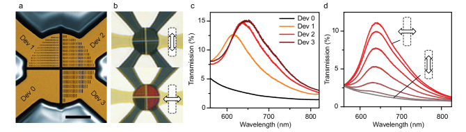
Fig. 1 illustrates the sample configuration. We photolithographically define a circular gold bottom electrode (1 nm Ti / 50 nm Au) that is subsequently nanostructured by focused ion beam milling (FIB). The bottom electrode is segmented into four quarter-circle electrodes, which are wired individually as shown in Fig. 2a. One electrode remains unstructured (Device 0) to serve as a reference, while the remaining three electrodes are structured into arrays of optical antennas in the form of rectangular slots. The distance between slots is kept constant at along both the long and short side of the rectangles while the nominal size of the slots is , and for Devices 1, 2 and 3, respectively. Exfoliated few-layer h-BN (here: 9 atomic layers, or ) is transferred on top of the bottom electrode. The device is finalized by the fabrication of a common gold top electrode (15 nm Au) via photolithography. For details on the fabrication process, see Methods and Supplementary Information, Section 1.
The optical properties of the final devices are shown in Fig. 2b-d. The transmission of light through the devices strongly depends on its (linear) polarization, as shown in Fig. 2b. Observing light polarized along the short axis of the slots results in a strong color contrast between devices. This contrast vanishes when observing light polarized along the long axis. The colors of the electrodes suggest that the slots enhance transmission in a certain spectral range. This observation is quantified in the transmission spectra shown in Fig. 2c. All structured devices exhibit characteristic resonances and enhanced transmission at wavelengths corresponding to the observed colors in Fig. 2b. The transmission peak shifts towards longer wavelengths as the aspect ratio of the slots is increased in accordance with Refs. kleinkoerkamp04 ; garciavidal05 . Fig. 2d shows the change in the transmitted spectrum as a function of polarizer angle. The resonance disappears when the analyzer is oriented along the long axis of the slots. The transmission follows a dependence (see Supplementary Information, Section 2) gordon04 .
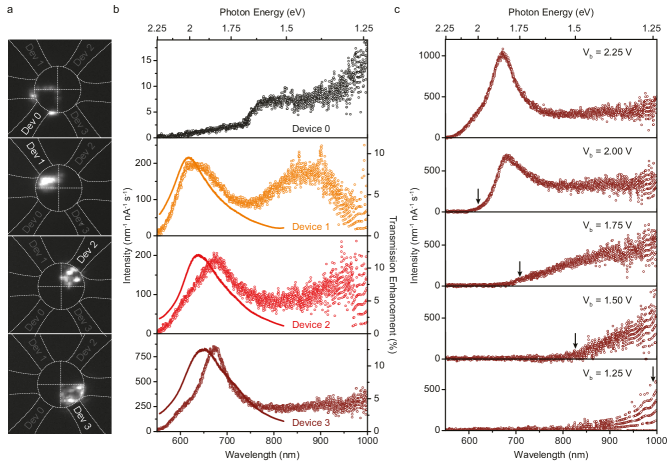
Next, we discuss the properties of photon emission induced by inelastic electron tunneling. The top-most image in Fig. 3a shows a real-space map of the light emitted from the unstructured reference device, recorded with a constant tunnel bias voltage of . Light emission is localized to the edges of the device. The spectrum of the emitted light, shown in Fig. 3b, is broad and without distinct features, falling off continuously towards shorter wavelengths. In the absence of slots, as is the case for the reference device, inelastically tunneling electrons predominantly interact with surface plasmon polaritons (SPPs) associated with the metal-insulator-metal (MIM) configuration miyazaki06 ; chen13 . In the absence of discontinuities, these modes cannot couple to free-space radiation because of the large momentum mismatch (c.f. Supplementary Information, Section 3.2). However, scattering due to surface roughness or edges provides the momentum required to overcome this mismatch.
In contrast, all devices with nanostructured bottom electrodes show light emission from the entire device area (Fig. 3a). As seen in the corresponding spectra in Fig. 3b, the antenna-coupled devices exhibit strongly enhanced light emission intensity, especially in the spectral domain of the transmission peaks discussed previously. The external electron-to-photon conversion efficiency is increased by two orders of magnitude from to at . A direct comparison of the transmission and emission spectra shows good agreement in spectral width and shape. However, the peaks observed in the light emission are red-shifted compared to the peaks in transmission. Numerical simulations, which will be discussed later on, suggest that this spectral shift is caused by the spectral dependence of electron-radiation coupling mediated by the slot antennas. The spatial non-uniformity of the emitted light intensity is due to fabrication-related contamination at the Au–h-BN interfaces and roughness of the polycrystalline electrodes to which the atomically flat h-BN crystal cannot conform perfectly britnell12a . Photon emission can be made spatially more uniform by using monocrystalline or template-stripped gold electrodes nagpal09 ; huang10b .
As reported by Lambe and McCarthy, inelastic electron tunneling results in broad-band light emission with a high-frequency cutoff given by
| (1) |
with being the photon energy, the electron charge and the tunnel bias voltage lambe76 . According to equation (1), the antenna-specific resonances should only be excitable if the applied bias exceeds the energy of the antenna mode. As shown in Fig. 3c, this behaviour is indeed observed. The figure renders light emission spectra for Device 3 as a function of applied bias . The experimental data shows good agreement with equation (1).
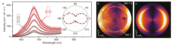
To understand the role of the slot antennas in the light generation process, we studied the polarization and radiation characteristics of the emitted light. Fig. 4a shows emission spectra for Device 3 as a function of polarizer angle. The light intensity is maximized when the polarizer is oriented parallel to the short axis of the slots. For a polarizer angle parallel to the long axis of the slots we observe a 80 % extinction. Fig. 4b shows the photon momentum distribution in the back focal plane of the microscope objective (NA 1.4). Light is preferentially emitted in -direction, i.e. parallel to the short axis of the slots. The measured polarization and the back focal plane intensity distribution qualitatively agree with the radiation generated by a magnetic dipole over a dielectric substrate novotny12 and oriented along the long axis of the slots (c.f. Fig. 4c). These results are in agreement with the notion that slots can be viewed – in terms of Babinet’s principle – as the complement of linear rod antennas, radiation from which is dominated by an electric dipole mode along the long axis of the rod yang14 . However, as will be discussed later, slots also support electric dipole resonances parallel to their short axis.
To establish an understanding of the electron-to-photon conversion efficiency and its spectral dependence, we express the spectrum of the emitted power as
| (2) |
with being the electron-to-plasmon conversion rate and the radiation efficiency of the antenna. is described by Fermi’s “golden rule” persson92 ; chen09b ; schneider13 and depends on the applied bias , the electronic density of states in the electrodes as well as the number of plasmonic modes that the electrons can couple to aizpurua00 . The latter corresponds to the local density of electromagnetic states (LDOS) in the MIM tunnel gap. The radiation efficiency denotes the efficacy of the slot antennas at converting the energy of MIM plasmons into free space radiation. We next discuss the spectral dependence of and for a slot antenna; see Supplementary Information, Section 4 for additional data.
We derive the LDOS seen by the tunneling electrons by numerically calculating the total dissipated power of a point dipole placed in the tunnel junction. The LDOS is then obtained by novotny12
| (3) |
where is the vacuum LDOS and is the radiated power of a dipole of equal dipole moment in a homogeneous dielectric environment.
Fig. 5b shows the normalized LDOS for a dipole placed at a distance of nm from the edge of an antenna slot (c.f. Fig. 5a). A large fraction of the LDOS is associated with MIM-SPP modes, which are ultimately dissipated to heat in the absence of antenna coupling (see Supplementary Information, Section 4.3).
In terms of the radiated power , the radiation efficiency can be expressed as
| (4) |
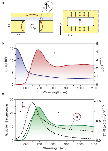
Fig. 5b renders as a function of wavelength for the dipole near the edge of an antenna slot. We find that the antenna converts SPP modes to propagating radiation most efficiently in a narrow spectral range centered at . This antenna resonance can be associated with radiative magnetic and electric dipole modes, as discussed below. By varying the lateral position of in the tunnel gap we can map out the total LDOS as well as the radiative LDOS as a function of proximity to the antenna slot.
The conversion of SPP modes to free-propagating radiation is most efficient for dipoles that are close to the antenna slot (see Supplementary Information, Section 4.3). Finally, this allows us to calculate the spectrum of the emitted power . The modeled spectrum for an applied bias of is shown in Fig. 5c. The spectral shape
agrees well with our measurements shown in Fig. 3b. For further details of the model and comparison to experimental data, see Supplementary Information, Section 4.5.
In order to understand the experimentally observed spectral shift between transmission and light emission resonances, as well as the magnetic dipole character of light emission, it is necessary to identify the nature and symmetry of electromagnetic modes supported by slot antennas.
Radiation from an aperture can be described by a multipole series, with the leading terms for small apertures being magnetic and electric dipoles.
As illustrated in Fig. 5a, we find that the dominating modes supported by slot antennas are an electric dipole mode along the short axis (), and a magnetic dipole mode parallel to the long axis () of the slot, in agreement with recent cathodoluminescence measurements coenen14 .
Resonances of both magnetic and electric dipolar modes red-shift with increasing slot aspect ratio, in accordance with both experimental transmission and light emission results (see Supplementary Information, Section 4.1). The dashed curves in Fig. 5c show numerically obtained mode spectra for and . The resonance is red-shifted with respect to the resonance. Furthermore, the resonance is asymmetric with a long-wavelength tail due to strong coupling to MIM-SPPs, the damping of which increases with decreasing wavelength.
Returning back to equation (2), we now realize that the spectral dependence of the antenna-coupled tunneling device is dictated by the intricate interaction of tunneling electrons and electromagnetic modes supported by the slot antennas.
As discussed earlier, our experimental results indicate that the enhanced light emission is mediated primarily by the magnetic dipolar antenna mode. This observation is substantiated by the spectral overlap of the emission spectrum with , as well as by the symmetry of this mode which favors field localization to the gap region. On the other hand, again for reasons of symmetry, linearly polarized far-field radiation primarily couples to in-plane electric dipole modes, i.e. the resonant enhancement of transmission through the device is mediated by the electric dipole mode . These conclusions are supported by the observed spectral shift between the transmission and emission peaks discussed earlier, which we also find between electric dipole mode spectrum and emission spectrum (c.f. Fig. 5c).
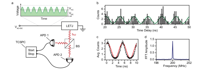
In a final experiment, we demonstrate the feasibility of ultrafast temporal modulation of light emission from h-BN tunnel junctions. As depicted in Fig. 6a, we drive the device with an RF signal of frequency , and record a histogram of the interphoton arrival times in the resulting photon stream by employing time-correlated single-photon counting (TCSPC). Fig. 6b shows an excerpt from such a histogram recorded for a modulation frequency of , demonstrating that the photon stream is indeed time-modulated at the same frequency . This can be seen unambiguously by averaging and Fourier-transforming the raw histogram, as shown in Figs. 6c,d. Following this approach, we have modulated photon emission from our devices at frequencies ranging from to . For a detailed discussion of the method and further results, see Supplementary Information, Section 5.2.
Further studies will be aimed at the increase of efficiencies through alternative antenna designs (e.g. patch antennas bigourdan14 or nanocube antennas akselrod14 ) and improvements in fabrication and materials. For example, MIM propagation lengths may be increased through the use of monocrystalline metals huang10b or alternative materials khurgin10 ; boltasseva11 ; tassin12 . Higher efficiencies and spectrally narrower resonances can also be achieved through MIM gap resonances.
Equivalent circuit models will help to improve impedance matching between the tunnel junction and free-space, thereby improving the device efficiency further alu08a ; greffet10a .
In conclusion, we have demonstrated optical antenna mediated conversion of electronic into optical energy in a solid-state system, and its modulation at frequencies up to 1 GHz. The vertical design of slot antennas allows for sub-nanometer control of gap-size and configuration, a goal which is difficult to achieve in traditional in-plane antenna designs. We find that arrays of slot antennas exhibit geometrically tunable, polarization-sensitive resonances that facilitate enhanced device transmission. While light emission from unstructured devices is weak and limited to the edges of the device, slot antenna arrays emit from the entire device area. The emitted light is strongly polarized along the short axis of the slots in correspondence with the polarization dependence of the transmission. The exploration of junction configurations based on van der Waals heterostructures geim13 with tailored electronic properties may lead to significant improvements in efficiencies and enable novel device functionalities. By reciprocity, the geometry presented in this study is also capable of converting far-field radiation into localized energy, which is of interest for photovoltaics, photodetection and optical sensors.
I Methods
I.1 Sample Fabrication
Devices are fabricated on commercially available glass coverslips (). Both bottom and top electrodes were fabricated by standard UV photolithography, electron-beam evaporation of titanium and gold targets, and subsequent lift-off. Bottom electrodes were nanostructured using a dual-beam FEI FIB Helios 600i. The top electrode of the device used in the frequency-modulation experiments was fabricated using a silicon nitride membrane shadow mask prepared by FIB milling.
h-BN crystals were grown as described in Ref. taniguchi07 . Few-layer h-BN atomic crystals were exfoliated on silicon wafers with a 280 nm oxide layer using the scotch-tape micromechanical cleavage technique novoselov04a ; novoselov05b . Crystals were identified by means of optical microscopy as well as atomic force microscopy using a Bruker Innova AFM in tapping mode.
The transfer was carried out as follows:
The Si/SiO2 substrate containing the h-BN crystals is partially covered with a commercial PDMS film (Gel-Film® PF-40-X4 supplied by Gel-Pak) in such a way that small margins along the edges of the substrate are left exposed.
The stack is subsequently floated on deionized water, the exposed (hydrophilic) Si/SiO2 surface is wetted such that a meniscus is formed around the hydrophobic PDMS and heated to . After the stack is completely immersed in water and the PDMS film is peeled-off under water. During this process the majority of h-BN crystals gets transferred from the Si/SiO2 to the PDMS. The PDMS film, carrying the h-BN crystal, is subsequently aligned manually with the bottom electrode using a SUSS MJB4 mask aligner, attached to a quartz carrier, and brought into contact with the bottom electrode. As the PDMS film is released from the sample, the h-BN crystal gets transferred onto the bottom electrode. See Supplementary Information for AFM and optical microscope images of the transfer process.
Samples were annealed in a tube furnace under a flow of Argon and Hydrogen at for before and after transfer.
I.2 Sample Characterization
All measurements were carried out on a customized, inverted Nikon TE300 microscope. For transmission measurements light from a supercontinuum source (NKT SuperK EXTREME) was focused onto the devices through a top objective (50x, NA 0.8). Transmitted light as well as light emitted by the devices was collected using an oil-immersion objective (100x, NA 1.4). Spectra of the transmitted as well as emitted light were acquired with an Acton SpectraPro 300i spectrometer. Transmission spectra are normalized by spectra acquired on glass, which is assumed to correspond to the theoretical value of 96 %. Units of light emission spectra are not arbitrary. They are normalized by the system efficiency, acquisition time and the average current flowing through the device during acquisition. The system response was calibrated using an OceanOptics HL-2000-CAL calibration lamp. Real space as well as back-focal plane images of the emitted light were acquired using an Andor iXon Ultra EMCCD camera. As a DC voltage source and for electrical measurements we used a Keithley 2602B source meter. The RF signal is generated by a Hewlett Packard 8648B signal generator. TCSPC histograms are acquired using a PicoQuant PicoHarp 300 module as well as two Excelitas Technologies SPCM-AQRH-14 APDs.
I.3 Numerical Simulations
Numerical finite-element simulations were carried out with COMSOL Multiphysics 4.4. We assumed refractive indices of 1.52 for glass and 1.8 for h-BN levinshtein01 . Empirical values were used for the dielectric function of gold johnson72 . The 1 nm adhesion layer of the lower electrode was not taken into account. Full-field simulations of the electromagnetic fields were performed for electric / magnetic point dipoles at the positions mentioned in the main text. The radiated power was extracted by integrating the time-averaged Poynting vector over the simulation boundaries in the lower and upper half-spaces. The non-radiative energy loss rate is calculated by integrating the total power dissipation density within the metallic domains. Perfectly matched layers were used as simulation boundaries.
References
- (1) Bharadwaj, P., Deutsch, B. & Novotny, L. Optical antennas. Adv. Opt. Phot. 1, 438 – 483 (2009).
- (2) Alù, A. & Engheta, N. Input impedance, nanocircuit loading, and radiation tuning of optical nanoantennas. Phys. Rev. Lett. 101, 043901 (2008).
- (3) Greffet, J.-J., Laroche, M. & Marquier, F. Impedance of a nanoantenna and a single quantum emitter. Phys. Rev. Lett. 105, 117701 (2010).
- (4) Novotny, L. & van Hulst, N. F. Antennas for light. Nature Photon. 5, 83–90 (2011).
- (5) Biagioni, P., Huang, J.-S. & Hecht, B. Nanoantennas for visible and infrared radiation. Rep. Prog. Phys. 75, 024402 (2012).
- (6) Schuller, J. A. et al. Plasmonics for extreme light concentration and manipulation. Nature Mat. 9, 193–204 (2010).
- (7) Mühlschlegel, P., Eisler, H.-J., Martin, O. J. F., Hecht, B. & Pohl, D. W. Resonant optical antennas. Science 308, 1607 (2005).
- (8) Curto, A. G. et al. Unidirectional emission of a quantum dot coupled to a nanoantenna. Science 329, 930–933 (2010).
- (9) Kinkhabwala, A. et al. Large single-molecule fluorescence enhancements produced by a bowtie nanoantenna. Nature Phot. 3, 654–657 (2009).
- (10) Atwater, H. A. & Polman, A. Plasmonics for improved photovoltaic devices. Nature Mat. 9, 205–213 (2010).
- (11) Tang, L. et al. Nanometre-scale germanium photodetector enhanced by a near-infrared dipole antenna. Nature Photon. 2, 226–229 (2008).
- (12) Knight, M. W., Sobhani, H., Nordlander, P. & Halas, N. J. Photodetection with active optical antennas. Science 332, 702–704 (2011).
- (13) Huang, K. C. et al. Electrically driven subwavelength optical nanocircuits. Nature Photon. 8, 244–249 (2014).
- (14) Lambe, J. & McCarthy, S. L. Light emission from inelastic electron tunneling. Phys. Rev. Lett. 37, 923 (1976).
- (15) Kirtley, J., Theis, T. & Tsang, J. Light emission from tunnel junctions on gratings. Phys. Rev. B 24, 5650 (1981).
- (16) Sparks, P., Sjodin, T., Reed, B. & Stege, J. Light emission from the slow mode of tunnel junctions on short period diffraction gratings. Phys. Rev. Lett. 68, 2668 (1992).
- (17) Gimzewski, J. K., Reihl, B., Coombs, J. H. & Schlittler, R. R. Photon emission with the scanning tunneling microscope. Z. Phys. B 72, 497–501 (1988).
- (18) Schull, G., Néel, N., Johansson, P. & Berndt, R. Electron-plasmon and electron-electron interactions at a single atom contact. Phys. Rev. Lett. 102, 057401 (2009).
- (19) Chen, C., Bobisch, C. A. & Ho, W. Visualization of Fermi’s Golden Rule through imaging of light emission from atomic silver chains. Science 325, 981 (2009).
- (20) Bharadwaj, P., Bouhelier, A. & Novotny, L. Electrical excitation of surface plasmons. Phys. Rev. Lett. 106, 226802 (2011).
- (21) Zhang, Y. et al. Edge scattering of surface plasmons excited by scanning tunneling microscopy. Opt. Expr. 21, 13938–13948 (2013).
- (22) Davis, L. Theory of surface-plasmon excitation in metal-insulator-metal tunnel junctions. Physical Review B 16, 2482 (1977).
- (23) Rendell, R. W. & Scalapino, D. J. Surface plasmons confined by microstructures on tunnel junctions. Phys. Rev. B 24, 3276–3294 (1981).
- (24) Johansson, P., Monreal, R. & Apell, P. Theory for light emission from a scanning tunneling microscope. Phys. Rev. B 42, 9210–9213 (1990).
- (25) Persson, B. N. J. & Baratoff, A. Theory of photon emission in electron tunneling to metallic particles,. Phys. Rev. B 68, 3224–3227 (1992).
- (26) Aizpurua, J., Apell, S. P. & Berndt, R. Role of tip shape in light emission from the scanning tunneling microscope. Phys. Rev. B 62, 2065–2073 (2000).
- (27) Landauer, R. & Martin, T. Barrier interaction time in tunneling. Rev. of Mod. Phys. 66, 217 (1994).
- (28) Shafir, D. et al. Resolving the time when an electron exits a tunnelling barrier. Nature 485, 343–346 (2012).
- (29) Ward, D. R., Hüser, F., Pauly, F., Cuevas, J. C. & Natelson, D. Optical rectification and field enhancement in a plasmonic nanogap. Nature Nanotech. 5, 732–736 (2010).
- (30) Lee, G.-H. et al. Electron tunneling through atomically flat and ultrathin hexagonal boron nitride. Appl. Phys. Lett. 99, 243114 (2011).
- (31) Britnell, L. et al. Electron tunneling through ultrathin boron nitride crystalline barriers. Nano Lett. 12, 1707–1710 (2012).
- (32) Watanabe, K., Taniguchi, T. & Kanda, H. Direct-bandgap properties and evidence for ultraviolet lasing of hexagonal boron nitride single crystal. Nature Mat. 3, 404–409 (2004).
- (33) Koerkamp, K. J. K., Enoch, S., Segerink, F. B., van Hulst, N. F. & Kuipers, L. Strong influence of hole shape on extraordinary transmission through periodic arrays of subwavelength holes. Phys. Rev. Lett. 92, 183901 (2004).
- (34) Garcia-Vidal, F., Moreno, E., Porto, J. & Martin-Moreno, L. Transmission of light through a single rectangular hole. Phys. Rev. Lett. 95, 103901 (2005).
- (35) Gordon, R. et al. Strong polarization in the optical transmission through elliptical nanohole arrays. Phys. Rev. Lett. 92, 037401 (2004).
- (36) Miyazaki, H. T. & Kurokawa, Y. Squeezing visible light waves into a 3-nm-thick and 55-nm-long plasmon cavity. Phys. Rev. Lett. 96, 097401 (2006).
- (37) Chen, X. et al. Atomic layer lithography of wafer-scale nanogap arrays for extreme confinement of electromagnetic waves. Nature Commun. 4, 2361 (2013).
- (38) Nagpal, P., Lindquist, N. C., Oh, S.-H. & Norris, D. J. Ultrasmooth patterned metals for plasmonics and metamaterials. Science 325, 594–597 (2009).
- (39) Huang, J. et al. Atomically flat single-crystalline gold nanostructures for plasmonic nanocircuitry. Nature Commun. 1, 150 (2010).
- (40) Novotny, L. & Hecht, B. Principles of Nano-Optics (Cambridge University Press, Cambridge, 2012), second edn.
- (41) Yang, H. U. et al. Accessing the optical magnetic near-field through babinet’s principle. ACS Photonics 1, 894–899 (2014).
- (42) Schneider, N. L., Johansson, P. & Berndt, R. Hot electron cascades in the scanning tunneling microscope. Phys. Rev. B 87, 045409 (2013).
- (43) Coenen, T. & Polman, A. Optical properties of single plasmonic holes probed with local electron beam excitation. ACS Nano 8, 7350–7358 (2014).
- (44) Bigourdan, F., Marquier, F., Hugonin, J.-P. & Greffet, J.-J. Design of highly efficient metallo-dielectric patch antennas for single-photon emission. Opt. Expr. 22, 2337–2347 (2014).
- (45) Akselrod, G. M. et al. Probing the mechanisms of large purcell enhancement in plasmonic nanoantennas. Nature Photon. 8, 835–840 (2014).
- (46) Khurgin, J. B. & Sun, G. In search of the elusive lossless metal. Appl. Phys. Lett. 96, 181102 (2010).
- (47) Boltasseva, A. & Atwater, H. A. Low-loss plasmonic metamaterials. Science 331, 290–291 (2011).
- (48) Tassin, P., Koschny, T., Kafesaki, M. & Soukoulis, C. M. A comparison of graphene, superconductors and metals as conductors for metamaterials and plasmonics. Nature Photon. 6, 259–264 (2012).
- (49) Geim, A. & Grigorieva, I. Van der waals heterostructures. Nature 499, 419–425 (2013).
- (50) Taniguchi, T. & Watanabe, K. Synthesis of high-purity boron nitride single crystals under high pressure by using Ba–BN solvent. Journal of crystal growth 303, 525–529 (2007).
- (51) Novoselov, K. S. et al. Electric field effect in atomically thin carbon films. Science 306, 666–669 (2004).
- (52) Novoselov, K. S. et al. Two-dimensional atomic crystals. Proc. Natl. Acad. Sci. USA 102, 10451 (2005).
- (53) Levinshtein, M. E., Rumyantsev, S. L. & Shur, M. S. Properties of Advanced Semiconductor Materials: GaN, AIN, InN, BN, SiC, SiGe (John Wiley & Sons, 2001).
- (54) Johnson, P. B. & Christy, R. W. Optical constants of the noble metals. Phys. Rev. B 6, 4370–4379 (1972).
II Acknowledgments
The authors thank Zachary J. Lapin for sample fabrication by focused ion beam milling, Karol Luszcz for support regarding the frequency modulation experiments as well as Mark Kasperczyk and Dieter W. Pohl for helpful discussions. Funding by the NCCR-QSIT program and the Swiss National Science Foundation (grant 200021_149433) is greatly appreciated. We further acknowledge the use of facilities at the FIRST Center for Micro- and Nanotechnology as well as the Scientific Center for Optical and Electron Microscopy (ScopeM) at ETH Zürich. K.W. and T.T. acknowledge support from the Elemental Strategy Initiative conducted by the MEXT, Japan. T.T. acknowledges support a Grant-in-Aid for Scientific Research on Grant 262480621 and on Innovative Areas ”Nano Informatics” (Grant 25106006) from JSPS.
III Author Contributions
L.N., P.B. and M.P. conceived the research. M.P. fabricated the samples and carried out the numerical simulations. M.P. and P.B. measured the samples. A.J. developed the
transfer technique. K.W. and T.T. synthesized the h-BN crystals. M.P, P.B. and L.N. discussed results and co-wrote the paper.