Impedance matching of inverted conductors: Two-dimensional beam splitters with divergent gain
Abstract
A thin conducting sheet — graphene, for example — transmits, absorbs, and reflects radiation. A sheet that is very thin, even vanishingly so, can still produce 50% absorption at normal incidence if it has conductivity corresponding to half the impedance of free space. We find that, regardless of the sheet conductivity, there exists a combination of polarization and angle of incidence that achieves this impedance half-matching condition. If the conducting medium can be inverted, the conductivity is formally negative and the sheet amplifies the incident radiation. To the extent that a negative half-match in a thin sheet can be maintained, enormous single-pass gain in both transmission and reflection is possible. Known semiconductors (e.g., gallium nitride) have the optical properties necessary to give large amplification in a structure that is, remarkably, both thin and nonresonant.
pacs:
42.79.Fm, 78.20.-e, 42.55.AhI Introduction
An electromagnetic medium can be characterized by its permittivity and permeability , or equivalently by its index of refraction and impedance Heald and Marion (1995). Metamaterials exhibiting the unusual case of a negative index can be engineered Veselago (1968) and show promise for previously unimagined applications such as perfect lenses Pendry (2000). Negative impedances are analogous to negative indices: while not the usual case, they are not forbidden. Materials with this property are prepared by creating a population inversion, and are widely used in lasers and other optical amplifiers Heald and Marion (1995). This communication describes how a negative-conductivity, properly impedance-matched thin sheet can form an amplifying beamsplitter with enormous single-pass gain.
Much like pellicle beamsplitters, these systems are thin films that divide an incident beam into transmitted and reflected components. The case of reflective amplification is particularly noteworthy, for, in the limit where the film becomes vanishingly thin, the reflection and amplification occur simultaneously upon incidence at the gain medium interface. This situation stands in marked contrast to other types of optical amplifiers, even those where reflection plays a conspicuous role in enhancing the gain. For instance, in disk lasers, also known as active mirrors, the gain can be attributed to one medium and the reflection to another Abate et al. (1981). Likewise in fibers with active cladding the gain is most easily viewed as occurring as the evanescent wave propagates in the gain medium Koester (1966). Here, in the thin film limit, the gain and reflection cannot be conceptually decoupled. Thus this classical example identifies a direct connection between reflection and stimulated emission.

II Sheet
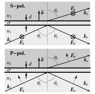
The reflection, transmission, and absorption of classical electromagnetic waves by a planar conductor is depicted in Fig. 1. We begin by treating the case of a conducting sheet of infinitesimal thickness, an algebraically simple but conceptually rich example which captures our main results. We imagine plane waves of angular frequency and wavevector incident on a sheet at an angle relative to the sheet normal vector (Fig. 1). Ohm’s law describes the coupling between the surface current density and the electric field . The two dimensional conductivity has the dimensionality of conductance, e.g., or . The third and fourth Maxwell equations give the non-redundant relations that follow from matching the fields at the boundary,
| (1a) | ||||
| (1b) | ||||
where we have used . For simplicity we take all of the materials in the problem to be non-magnetic, with permeability . Solving these equations with the sign conventions shown in Fig. 1 gives
| (2a) | ||||
| (2b) | ||||
| (2c) | ||||
| (2d) | ||||
where and refer to the normalized ratios of the reflected and transmitted electric fields for the two polarizations and ( and the plane of incidence respectively). Here is the impedance of free space, and for the dissipationless, semi-infinite boundary media . The angles of incidence, reflection, and transmission have been re-written as and , where and are related by Snell’s law, . When the sheet has zero conductivity (), the expressions (2) properly reduce to the usual Fresnel equations describing transmission and reflection at the interface between two dielectrics.
Energy conservation gives , which relates the absorption () to the reflection () and transmission () power ratios. For the case where the medium is the same on both sides of the sheet, and . The results for both polarizations can then be summarized,
| (3) |
where we have defined effective conductivity ratios
| (4a) | ||||
| (4b) | ||||
for -polarization and -polarization respectively. Equations (3) and (4), plotted in Fig. 2, capture the main results of this paper.
To elucidate the implications of Eqs. (3) and (4) we take and first consider the case of normal incidence (). Even for the usual case of positive conductivity (), Eq. (3) shows interesting behavior. As expected, for vanishing conductivity the transmission and the reflection , whereas for high conductivity and . The absorption vanishes in both limits, but the intermediate maximum is surprisingly large. As has been noted previously Woltersdorff (1934); Kaplan (1964); Bosman et al. (2003); Kaplan and Zeldovich (2006), a sheet with half the impedance of free space absorbs 50% of the incident power at normal incidence, even if it is thin compared to a skin depth. The 50% limit on the absorption results from the lack of dissipative coupling to the magnetic half of the electromagnetic wave’s energy Yu and Capasso (2014), but excepting this factor of two the coupling is maximal.
Proceeding to the case of non-normal incidence, we see that, because of the cosines in Eqs. (4), varying the polarization and angle of incidence can accomplish the same result as varying the conductivity . Working in -polarization (-polarization) away from normal incidence effectively increases (decreases) the sheet conductivity. To the extent that glancing incidence () can be achieved, any effective conductivity ratio is possible regardless of the actual sheet conductivity . As a consequence, maximal coupling can be arranged in any one of the transmission, absorption, or reflection channels.
Particularly important is the geometry that gives strong coupling in the absorption channel. A sheet with, for example, low conductivity can be made to achieve maximal by arranging an angle of incidence in -polarization. If this impedance-matching condition is satisfied with positive conductivity, then and . Such large absorption in a thin layer could help improve the economics of solar cells, for instance.
With an inverted, or negative-conductivity, sheet, achieving the corresponding maximal coupling condition, , gives extraordinary behavior. In this case , , and are all divergent, with and positive and negative (see Fig. 2). As the sheet effectively becomes an amplifying 50:50 beamsplitter with large gain in both the transmitted and the reflected beams.
As in the case of positive conductivity, the effective conductivity ratio can be tuned geometrically, perhaps to achieve a certain impedance match Yu and Capasso (2014). If for technical reasons creating a highly-conductive, inverted medium is difficult, larger negative can still be achieved by working at glancing incidence in -polarization. For both conductivity cases the geometric tuning is nontrivial, i.e., not a Lambertian cosine dependence resulting from changes in the sheet’s projected area Mecklenburg et al. (2010).
Normally one thinks of gain as being equivalent to negative absorption. While true, this viewpoint easily leads to the erroneous conclusion that weakly absorbing materials have limited potential for producing large, single-‘pass’ gain. Here we might expect that the 50% absorption limit would imply a maximum gain of or . In contrast with this naïve expectation, the amplification produced by an inverted medium can be much larger than the corresponding attenuation produced by the uninverted medium. Changing the sign of the conductivity is not equivalent to changing the sign of the absorption.
Qualitatively the two-dimensional (2D), negative-conductivity sheet with has a unique feature: it gives gain which cannot be accredited to the process of transmission through an inverted medium, but rather occurs during reflection at an interface. A quantum-mechanical description of this process must necessarily identify reflection as a form of stimulated emission. Typically stimulated emission is considered to create a new photon with quantum numbers identical to those of the incident photon, but with reflection this identity can no longer hold; one component of the new photon’s momentum must have sign opposite that of the incident photon.
The potential divergence seen in Eq. (3) is reminiscent of the one occurring in a Fabry-Perot resonator with cavity gain greater than its round-trip losses, where it is indicative of self-oscillation Verdeyen (1995). In this analogy the amplifying beamsplitter corresponds to the zero-mode of a Fabry-Perot etalon, with no cavity or resonant structure. As in a laser, the pump process maintaining the negative conductivity only supplies energy at a limited rate, so in an actual physical implementation divergent gain will not be achieved. The magnitude of will decrease as the amplification rate approaches the pump rate. Nonetheless exploring the origin of this infinity is instructive. As is so often the case, the formal divergence here can be traced to an unphysical geometric assumption: we have taken the conducting sheet to have zero thickness, while requiring that its conductivity remain finite. While at times a conducting sheet can be considered to be infinitely thin in the first approximation, this simplification gives quantitatively inaccurate results near .
III Slab
To treat the problem more realistically we apply the method of transfer matrices Jackson (1999) to a slab of conducting material of finite thickness. (We use the terms sheet and slab as shorthand for the infinitesimally thin layer calculated above and the finite thickness case treated below respectively.) Using this method the relationship between the incident, reflected, and transmitted electric fields can be written as
| (5) |
The matrix effecting the transformation is built up from a series of matrices, each describing the transfer across an interface or through some thickness of a medium. For the case of an incident wave from a medium (1) entering a second (2) and continuing on to a third (3), the transfer matrix has the form , where the translation matrix and the interface matrices account for the slab and boundaries designated by the respective subscripts. The procedure for generalizing such an expression to allow for an arbitrary number of finite-thickness slabs with different electromagnetic properties follows from induction and can be deduced by inspection. The matrix that evolves the wave across the th slab of thickness and index is
| (6) |
where . For -polarization the matrix enforcing the boundary conditions at an interface between two distinct media and is
| (7) |
Here the ’s and the ’s refer to the refractive indices and propagation angles (determined by Snell’s law) in the respective media. For -polarization has a similar form,
| (8) |
Explicit though lengthy expressions for , , and are easily found using Eqs. (5)–(8) given above.
To see the approach to the case of a conducting sheet in vacuum discussed previously, we take , and the slab’s refractive index to be given by
| (9) |
where is the complex permittivity and is the vacuum wavelength of the incident radiation. The three-dimensional (3D) conductivity in the limit . For -polarization, which is the more interesting case since invertible materials generally have small conductivities,
| (10) |
with . Assuming an index match () and a small phase (i.e., a thin slab) gives
| (11) |
where , , and we have kept terms to third order in in the denominator. At , which corresponds to the infinite gain condition () of the sheet case, this expression gives, to leading order, , where
| (12) |
Arranging gives an even larger , a result found by keeping terms to fifth order in . Thus the gain from a slab is finite for non-vanishing thickness , and diverges as with fixed.
The reflection gain of the slab arrangement (12) contrasts with the analogous result for the interface of two semi-infinite media, where the second one is active. There in all cases Siegman (2010); Perez et al. (2012). An infinitely thick inverted medium produces zero gain in reflection, while a thin, inverted medium can produce large .
That a thin slab can produce large is also surprising, since in typical optical amplifiers the small signal gain (in transmission, of course) grows exponentially as the gain medium thickness increases Verdeyen (1995); Silfvast (2003). This last point highlights the utility of an extended concept of impedance matching for negative-conductivity systems. Here, as a function of the conductivity and the thickness, the gain peaks at the negative analog of the best impedance match.
The role of impedance matching provides another perspective on the distinction between the amplifying beamsplitter and previously described optical amplifiers. The active mirror, for instance, is inherently a multipass transmission device Abate et al. (1981) that relies on an impedance mismatch to produce reflection. Likewise, amplifier designs based on total internal reflection, from fiber lasers Koester (1966) to whispering-gallery-mode microsphere lasers Sandoghdar et al. (1996), require an impedance mismatch in the form of an index discrepancy to produce reflection. The amplifying beamsplitter works best in the limit where an impedance half match, modulo a sign, is achieved.
IV Real materials
Although arranging the inversion and geometry to give in a thin layer might be technically challenging, in a physical implementation with real materials the gain described by Eq. (12) could be made large. As a first example we consider graphene, the canonical example of a thin conductor or “quantum membrane” Fang et al. (2013). Graphene has a two-dimensional optical conductivity
| (13) |
where is the fine structure constant, and and are the occupations of the valence and conduction bands respectively Mecklenburg et al. (2010). If doping and thermal excitations are negligible, then and and this expression reduces to the famous result connecting the optical conductivity to the absorption Ando et al. (2002); Nair et al. (2008). Partial inversion of graphene has been achieved with strong photoexcitation Li et al. (2012); Gierz et al. (2013). Assuming a complete inversion, a graphene thickness of 0.34 nm, and incident radiation with nm, Eq. (12) gives gains in transmission and reflection of . While such an inversion is unlikely to be realized in graphene, transition-metal dichalcogenides and other 2D layered semiconductors (e.g., WSe2) are similarly thin, with similar conductivities Fang et al. (2013), and can support practical inversions Wu et al. (2015). Thus such direct band gap materials show promise for realizing large gain.
Compared to many invertible materials these 2D layered semiconductors are good conductors at optical frequencies, but graphene — to continue using this example — only achieves the maximum coupling condition in -polarization at the glancing angle . If low conductivity makes inconveniently close to , the angle of incidence corresponding to maximal coupling can be decreased by working in very low index materials, e.g., photonic crystals Dowling and Bowden (1994); Gralak et al. (2000), or by increasing the ratio of to . Moving into the total internal reflection regime, however, gives an impedance mismatch that destroys the beamsplitter and spoils the system gain.
Standard invertible materials are characterized by their gain coefficients , which are related to optical conductivities by when [see Eq. 9] Heald and Marion (1995). Ruby, neodymium-doped yttrium aluminum garnet (Nd:YAG), neodymium-doped yttrium orthovanadate (Nd:YVO4), and titanium-doped sapphire have gain coefficients in the range 1–10 cm-1 Silfvast (2003); Bernard et al. (1994), making them more than times less conductive than graphene. The resulting angles of incidence are so near that a physical optics picture may be required. However, semiconducting materials can have gain coefficients as large as – cm-1 Shaklee et al. (1973), and crystalline monolayers are starting to see use as laser gain media Wu et al. (2015). Taking 20 nm of index-matched, low-temperature gallium nitride (GaN, , cm-1, nm) as an example Dingle et al. (1971), we find at , an angle that can be straightforwardly arranged. Decreasing the thickness or the gain coefficient gives larger gain at a larger angle; nm gives at , while cm-1 gives at . Known materials have the optical properties required to create a thin (), amplifying beamsplitter with large gain.
Despite appearances in these glancing incidence examples, waveguide effects are not involved: with a good inverted conductor one could achieve large gain at normal incidence. Lead telluride (PbTe) has near nm Suzuki and Adachi (1994), corresponding to a skin depth nm. At normal incidence such material in a slab of thickness nm in vacuum would give %, and if it could be fully inverted. As mentioned earlier, saturation effects limit the gain in practical situations, so such large should be taken to indicate nearly ideal coupling only.
Acknowledgements.
This work has been supported by NSF award DMR-1206849.References
- Heald and Marion (1995) Mark A. Heald and Jerry B. Marion, Classical Electromagnetic Radiation (Saunders College Pub., Fort Worth, 1995).
- Veselago (1968) Viktor G Veselago, “The electrodynamics of substances with simultaneously negative values of and ,” Soviet Physics Uspekhi 10, 509 (1968).
- Pendry (2000) J. B. Pendry, “Negative Refraction Makes a Perfect Lens,” Physical Review Letters 85, 3966–3969 (2000).
- Abate et al. (1981) J. A. Abate, L. Lund, D. Brown, S. Jacobs, S. Refermat, J. Kelly, M. Gavin, J. Waldbillig, and O. Lewis, “Active mirror: A large-aperture medium-repetition rate Nd:glass amplifier,” Applied Optics 20, 351–361 (1981).
- Koester (1966) C. Koester, “9A4 - Laser action by enhanced total internal reflection,” IEEE Journal of Quantum Electronics 2, 580–584 (1966).
- Woltersdorff (1934) Wilhelm Woltersdorff, “Über die optischen Konstanten dünner Metallschichten im langwelligen Ultrarot,” Zeitschrift für Physik 91, 230–252 (1934).
- Kaplan (1964) A. E. Kaplan, “On the reflectivity of metallic films at microwave and radio frequencies,” Radio Engineering and Electronic Physics 9, 1476–1481 (1964).
- Bosman et al. (2003) H. Bosman, Y. Y. Lau, and R. M. Gilgenbach, “Microwave absorption on a thin film,” Applied Physics Letters 82, 1353–1355 (2003).
- Kaplan and Zeldovich (2006) A. E. Kaplan and B. Ya. Zeldovich, “Free-space terminator and coherent broadband blackbody interferometry,” Optics Letters 31, 335 (2006).
- Yu and Capasso (2014) Nanfang Yu and Federico Capasso, “Flat optics with designer metasurfaces,” Nature Materials 13, 139–150 (2014).
- Mecklenburg et al. (2010) Matthew Mecklenburg, Jason Woo, and B. C. Regan, “Tree-level electron-photon interactions in graphene,” Physical Review B 81, 245401 (2010).
- Verdeyen (1995) Joseph T. Verdeyen, Laser Electronics, 3rd ed. (Prentice Hall, Englewood Cliffs, N.J, 1995).
- Jackson (1999) John David Jackson, Classical Electrodynamics, 3rd ed. (Wiley, New York, 1999).
- Siegman (2010) Anthony Siegman, “Fresnel Reflection, Lenserf Reflection and Evanescent Gain,” Optics and Photonics News 21, 38–45 (2010).
- Perez et al. (2012) Liliana I. Perez, Claudia L. Matteo, Javier Etcheverry, and María Celeste Duplaá, “Active isotropic slabs: Conditions for amplified reflection,” Journal of Optics 14, 125711 (2012).
- Silfvast (2003) William T. Silfvast, “Lasers,” in Fundamentals of Photonics, edited by Arthur Guenther, Leno S. Pedrotti, and Chandrasekhar Roychoudhuri (SPIE, Bellingham, 2003) pp. 1–45.
- Sandoghdar et al. (1996) V. Sandoghdar, F. Treussart, J. Hare, V. Lefevre-Seguin, J. M. Raimond, and S. Haroche, “Very low threshold whispering-gallery-mode microsphere laser,” Physical Review A 54, R1777–R1780 (1996).
- Fang et al. (2013) Hui Fang, Hans A. Bechtel, Elena Plis, Michael C. Martin, Sanjay Krishna, Eli Yablonovitch, and Ali Javey, “Quantum of optical absorption in two-dimensional semiconductors,” Proceedings of the National Academy of Sciences 110, 11688–11691 (2013).
- Ando et al. (2002) T. Ando, Y. S. Zheng, and H. Suzuura, “Dynamical conductivity and zero-mode anomaly in honeycomb lattices,” Journal of the Physical Society of Japan 71, 1318–1324 (2002).
- Nair et al. (2008) R. R. Nair, P. Blake, A. N. Grigorenko, K. S. Novoselov, T. J. Booth, T. Stauber, N. M. R. Peres, and A. K. Geim, “Fine structure constant defines visual transparency of graphene,” Science 320, 1308–1308 (2008).
- Li et al. (2012) T. Li, L. Luo, M. Hupalo, J. Zhang, M. C. Tringides, J. Schmalian, and J. Wang, “Femtosecond Population Inversion and Stimulated Emission of Dense Dirac Fermions in Graphene,” Physical Review Letters 108, 167401 (2012).
- Gierz et al. (2013) Isabella Gierz, Jesse C. Petersen, Matteo Mitrano, Cephise Cacho, I. C. Edmond Turcu, Emma Springate, Alexander Stöhr, Axel Köhler, Ulrich Starke, and Andrea Cavalleri, “Snapshots of non-equilibrium Dirac carrier distributions in graphene,” Nature Materials 12, 1119–1124 (2013).
- Wu et al. (2015) Sanfeng Wu, Sonia Buckley, John R. Schaibley, Liefeng Feng, Jiaqiang Yan, David G. Mandrus, Fariba Hatami, Wang Yao, Jelena Vučković, Arka Majumdar, and Xiaodong Xu, “Monolayer semiconductor nanocavity lasers with ultralow thresholds,” Nature 520, 69–72 (2015).
- Dowling and Bowden (1994) Jonathan P. Dowling and Charles M. Bowden, “Anomalous Index of Refraction in Photonic Bandgap Materials,” Journal of Modern Optics 41, 345–351 (1994).
- Gralak et al. (2000) Boris Gralak, Stefan Enoch, and Gérard Tayeb, “Anomalous refractive properties of photonic crystals,” Journal of the Optical Society of America A 17, 1012–1020 (2000).
- Bernard et al. (1994) J. E. Bernard, E. McCullough, and A. J. Alcock, “High gain, diode-pumped Nd:YVO4 slab amplifier,” Optics Communications 109, 109–114 (1994).
- Shaklee et al. (1973) KL Shaklee, RE Nahory, and RF Leheny, “Optical gain in semiconductors,” Journal of Luminescence 7, 284–309 (1973).
- Dingle et al. (1971) R Dingle, KL Shaklee, RF Leheny, and RB Zetterstrom, “Stimulated Emission and Laser Action in Gallium Nitride,” Applied Physics Letters 19, 5 (1971).
- Suzuki and Adachi (1994) Norihiro Suzuki and Sadao Adachi, “Optical Properties of PbTe,” Japanese Journal of Applied Physics 33, 193 (1994).