Influence of elastically pinned magnetic domain walls on magnetization reversal in multiferroic heterostructures
Abstract
In elastically coupled multiferroic heterostructures that exhibit full domain correlations between ferroelectric and ferromagnetic sub-systems, magnetic domain walls are firmly pinned on top of ferroelectric domain boundaries. In this work we investigate the influence of pinned magnetic domain walls on the magnetization reversal process in a Co40Fe40B20 wedge film that is coupled to a ferroelectric BaTiO3 substrate via interface strain transfer. We show that the magnetic field direction can be used to select between two distinct magnetization reversal mechanisms, namely (1) double switching events involving alternate stripe domains at a time or (2) synchronized switching of all domains. Furthermore, scaling of the switching fields with domain width and film thickness is also found to depend on field orientation. These results are explained by considering the dissimilar energies of the two types of pinned magnetic domain walls that are formed in the system.
I Introduction
The magnetic properties of a ferromagnetic film are determined by the relationship between intrinsic material parameters, such as exchange stiffness and magnetocrystalline anisotropy, and extrinsic effects, including magnetic anisotropies induced by shape, strain and interfaces. Typically, both intrinsic and extrinsic contributions give rise to a magnetic energy landscape that is uniform across the ferromagnetic film, aside from local variations caused by defects and/or film roughness. The magnetization reversal process and the magnetic hysteresis loop do not therefore usually depend on probing area. In conventional magnetic films with uniform magnetic anisotropy, magnetic switching proceeds by nucleation of reversed domains and subsequent domain growth via lateral domain wall motion. Models describing thermally activated magnetization reversal and magnetic domain wall motion use parameters that vary with magnetic anisotropy energy and random fluctuations thereof, while the energetics of magnetic domain walls is not specifically taken into account Labrune et al. (1989); Bruno et al. (1990); Lemerle et al. (1998). Since the density of domain walls is often low and their spin structure and energy remain nearly constant during domain growth, this omission is justified for most ferromagnetic systems. However, if the motion of magnetic domain walls is prohibited by strong pinning, the energetics of domain walls can have a more pronounced influence on magnetization reversal, especially when the density of pinned walls is high and the anisotropy axes in neighbouring domains are non-collinear.
Strong local pinning of magnetic domain walls can be attained by various methods, including focused ion beam or low-energy proton irradiation Chappert et al. (1998); Terris et al. (1999); Fassbender et al. (2004); Fassbender and McCord (2008); Franken et al. (2012); Kim et al. (2012); Hamann et al. (2014) and oxygen ion migration from an adjacent metal-oxide layer Bauer et al. (2013, 2015). Other promising strategies to locally tailor the magnetic properties of a continuous magnetic medium exploit exchange coupling with a multiferroic BiFeO3 layer Chu et al. (2008); Lebeugle et al. (2009); Heron et al. (2011); You et al. (2013) or strain coupling to the ferroelastic domains of a ferroelectric BaTiO3 substrate Lahtinen et al. (2011, 2012); Franke et al. (2012); Chopdekar et al. (2012); Streubel et al. (2013); Franke et al. (2014). In both cases, one-to-one correlations between the domains in BiFeO3 or BaTiO3 and the domains of an adjacent ferromagnetic film have been demonstrated. Furthermore, since the magnetic domain walls are firmly pinned on top of ferroelectric domain boundaries by abrupt changes in magnetic anisotropy, they do not move during magnetization reversal Lahtinen et al. (2011, 2012). This strong pinning effect leads to the formation of two types of magnetic domain walls with considerably different energy, depending on the direction of in-plane magnetic field Franke et al. (2012, 2014).
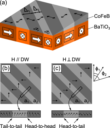
In this work we investigate the influence of pinned magnetic domain walls on magnetization reversal in a strain-coupled Co40Fe40B20/BaTiO3 heterostructure with regular magnetic stripe domains (Fig. 1). We find that magnetic switching in this system depends strongly on the type of magnetic domain wall that is created during a magnetic field sweep, especially if the thickness of the CoFeB film exceeds 50 nm. For magnetic fields along the stripe domains, high-energy head-to-head and tail-to-tail domain walls form. In this case, magnetization reversal proceeds in two clear steps involving abrupt magnetic switching in every second stripe domain at a time. The regular lateral modulations in the magnetization reversal process are driven by transformations of the domain wall structure into a low-energy head-to-tail configuration. On the other hand, if the magnetic field is applied perpendicular to the stripe domains, low-energy head-to-tail domain walls form. As a consequence, domain wall transformations cannot reduce the energy of the system and the magnetization of each domain switches simultaneously. The dependence of the magnetic switching fields for both reversal mechanisms on CoFeB film thickness and stripe domain width are discussed in detail.
II Experimental details
The experiments were conducted on a multiferroic heterostructure composed of a ferroelectric BaTiO3 (001) single-crystal substrate and a ferromagnetic Co40Fe40B20 wedge film, with thickness = 0 – 150 nm. The wedge film was deposited via magnetron sputtering at 300 ∘C. Upon cooling through the paraelectric-to-ferroelectric phase transition at 120 ∘C, the lattice structure of BaTiO3 becomes tetragonal and regular a1 – a2 ferroelastic stripe domains are formed to minimize electrostatic and elastic energies Merz (1954). The alternating 90∘ in-plane rotations of the lattice tetragonality that are characteristic of this domain pattern give rise, via inverse magnetostriction, to corresponding 90∘ in-plane rotations of the uniaxial magnetoelastic anisotropy axis in the CoFeB film.
At room temperature the ferroelastic a1 and a2 stripe domains are found to be fully imprinted into the CoFeB wedge film at all thicknesses, as schematically illustrated in Fig. 1(a). This indicates that the magnetoelastic anisotropy dominates over the other anisotropy contributions in CoFeB even at the thick side of the film.
The ferromagnetic domains were imaged at room temperature using magneto-optical Kerr effect (MOKE) microscopy with in-plane magnetic field. Magnetic hysteresis loops of individual a1 and a2 stripe domains were extracted from the variation of local magnetic contrast during magnetization reversal.
III Magnetically charged and uncharged domain walls
The magnetic domain walls that separate the imprinted a1 and a2 domains in CoFeB are strongly pinned onto the ferroelectric domain boundaries by the sudden rotation of the uniaxial magnetic anisotropy axes. As a result of this pinning effect, the magnetic domain walls do not move under application of a magnetic field and the total spin rotation within the walls varies with the direction and strength of the in-plane magnetic field Franke et al. (2012). Particularly relevant to the present work is the possibility to initialize magnetic domain walls with two distinct spin structures for specific magnetic field orientations. When the field is reduced from saturation along the direction parallel to the walls, the spins align in alternating head-to-head and tail-to-tail configurations which induce magnetostatic charges on each side of the domain walls (Fig. 1(b)). Accordingly, these domain walls are usually referred to as magnetically charged. On the other hand, when the field is reduced from saturation along the direction perpendicular to the walls, magnetically uncharged head-to-tail domain walls are instead formed (Fig. 1(c)). In ferromagnetic films without anisotropy modulations charged walls typically arrange in zigzag configurations to reduce magnetostatic charge density Hubert (1979); Hubert and Schäfer (1998); Favieres et al. (2013). In our strain-coupled multiferroic heterostructure, however, both magnetically charged and uncharged walls are perfectly straight because of strong pinning onto the underlying ferroelectric domain boundaries.
The profile of charged magnetic domain walls is mostly determined by the competition between magnetostatic energy and magnetic anisotropy energy, while exchange energy and magnetic anisotropy energy mainly define the structure of uncharged magnetic domain walls Franke et al. (2014). As magnetostatic coupling between spins extends over a longer distance than exchange interactions, the width and energy of charged walls are considerably larger than that of uncharged walls. Moreover, since the magnetostatic energy increases with ferromagnetic film thickness, the difference between the width and energy of charged and uncharged domain walls becomes more pronounced for thick filmsFranke et al. (2014).
Fig. 2(a) and (b) show Scanning Electron Microscopy with Polarization Analysis (SEMPA) images of charged and uncharged magnetic domains walls, at remanence, in a 20 nm CoFeB film that was grown on BaTiO3 under the same conditions as the wedge film.
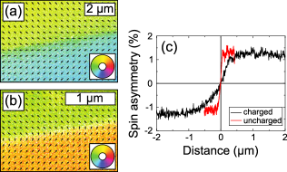
The elevated spatial resolution of SEMPA Berger and Oepen (1992); Frömter et al. (2011) allows for domain wall imaging at the nanoscale and for the extraction of the corresponding wall profiles (Fig. 2(c)). Following the domain wall width definition of Lilley Lilley (1950), the widths of the charged and uncharged domain walls are estimated as nm and nm, respectively.
IV Results and discussion
The magnetization reversal process in CoFeB under the formation of charged or uncharged domain walls is investigated by MOKE microscopy. To this end, a large set of MOKE images is collected as a function of magnetic field strength. This is done with the magnetic field applied either parallel or perpendicular to the domain walls and for different CoFeB film thicknesses. For each field sweep, the MOKE intensity of individual images is averaged along the direction of the stripe domains and combined into a single contour plot, as illustrated in Fig. 3.
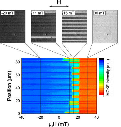
Such contour plots, wherein a vertical line contains information about the magnetization direction of each MOKE image, are used here as an efficient way to visualize magnetic switching in all the domains of the original set of images.
MOKE contour plots with magnetic field applied either parallel or perpendicular to the domain walls are shown in Fig. 4 for CoFeB film thicknesses ranging between 25 nm and 150 nm. To facilitate direct comparisons, the magnetic hysteresis loops of selected a1 and a2 domains are also shown. The width of the selected a1 and a2 domains is similar for all thicknesses, being on average µm and µm, respectively.
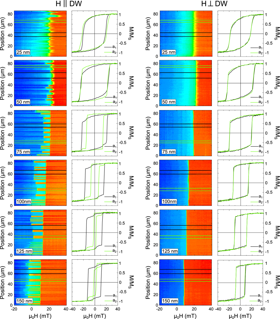
In both cases, the magnetic field is applied at an angle of 45∘ with respect to the easy axes of a1 and a2 domains (see Fig. 1). The reversal process should therefore not depend on the field direction nor the domain type, in accordance with the Stoner–Wohlfarth model for single domains with uniaxial magnetic anisotropy. In our system, however, the magnetic switching behavior depends strongly on the direction of the magnetic field and, for field parallel to the walls, on the domain type. In particular, a1 and a2 domains switch simultaneously when the magnetic field is applied perpendicularly to the walls, while they switch at distinct fields when the magnetic field is applied parallel to the walls. This unusual switching behavior is caused by strong magnetic domain wall pinning and the substantial energy difference between charged and uncharged walls Hubert (1979); Franke et al. (2014), as discussed below.
The influence of the two types of domain walls on the reversal process is clarified through consideration of individual MOKE images illustrating the switching of a1 and a2 domains at a specific thickness ( = 75 nm), as shown in Fig. 5.
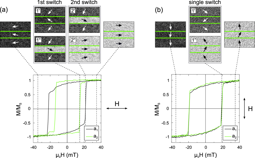
When the magnetic field is applied parallel to the walls (Fig. 5(a)) and reduced from saturation, the magnetization of each stripe domain rotates towards the respective easy anisotropy axes, causing the formation of charged domain walls. Both the energy and width of these walls are initially small, but rapidly increase upon decreasing field strength. At some field value (Fig. 5(a–)), the energy of charged walls becomes so large that an abrupt magnetic switching event is triggered in every second stripe domain (Fig. 5(a–)), here defined as a2. During this first switching event all charged domain walls transform into lower-energy uncharged domain walls, thus providing a net energy gain for the entire magnetic system. Upon a further increase of the magnetic field strength, the a1 domains switch too: during this second switching event all uncharged walls (Fig. 5(a–) are transformed back into charged walls (Fig. 5(a–)) which are now characterized by a modest spin rotation and, thus, considerably smaller energy. A different reversal process occurs when the magnetic field is applied perpendicular to the domain walls (Fig. 5(b)): now, uncharged walls are formed when the magnetic field is reduced from saturation and the magnetic system cannot reduce its energy by domain wall transformations. Instead, in order to prevent the formation of higher-energy charged walls, magnetic switching is now completely synchronized in all domains (Fig. 5(a–) and (a–)). A much weaker dependence of the magnetic hysteresis curve on the direction of applied magnetic field has been reported for an exchange-coupled La0.7Sr0.3MnO3/BiFeO3 heterostructure You et al. (2013).
IV.1 Scaling of magnetic switching with domain width
An intriguing aspect that emerges from the contour plots in Fig. 4 is the influence of domain width on the magnetization reversal process. When the magnetic field is applied along the stripe domains, charged walls are created and the switching field of the a2 domains () decreases with decreasing width . Specifically, is inversely proportional to , as illustrated in Fig. 6(a) for = 75 nm. This scaling behavior is explained considering that narrow a2 domains correspond to a higher density of charged domain walls and, consequently, a higher magnetic energy density compared to wide a2 domains. An alternative way to understand this behavior is provided in Fig. 6(b), where the value of the spin rotation of charged walls, measured just before the first switching event, is plotted as a function of , for = 75 nm. For = 5 µm the spin rotation of charged domain walls increases up to before switching, while in narrower a2 domains charged walls with considerably smaller spin rotation already transform into uncharged walls. Because larger spin rotations are associated with higher magnetic energy, Fig. 6(b) indicates that wider a2 domains can accommodate charged domain walls with higher energy than narrow a2 domains, before transformations to uncharged domain walls occur.
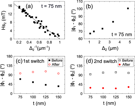
While scales with when the field is applied along the stripe domains, is independent of . Considering the arguments that were provided to explain the dependence of on , this circumstance may appear in contradiction with the fact that uncharged walls are transformed back into charged walls when a1 domains switch (see the second switching event in Fig. 5 (a)). However, charged walls that form after the second switching event have much smaller spin rotations, and correspondingly lower magnetic energies, than the charged walls before the first switching event. This is illustrated in Figs. 6 (c) – (d), where the spin rotation of charged and uncharged walls before and after the two switching events is plotted as a function of CoFeB film thickness, for a2 domains with similar width µm (a1 and a2 domains switch almost simultaneously for 50 nm and the corresponding data have been omitted from these figures). Since the energy of charged walls is small after magnetic switching in the a1 domains, is mainly determined by the magnetic anisotropy inside the domain, which is independent of , rather than the energetics of the domain walls. This observation is also confirmed by the fact that is nearly identical for the two field orientations (see Fig. 4).
IV.2 Scaling of magnetic switching with CoFeB film thickness
Finally, the dependence of the magnetic switching field on CoFeB film thickness is discussed. From Fig. 4 it can be seen that both and decrease with CoFeB thickness for t 50 nm. The switching fields of a1 domains (irrespective of field direction) and a2 domains (magnetic field perpendicular to the walls) are not drastically influenced by domain wall transformations and thus their variation with film thickness mimics that of ferromagnetic films without regular anisotropy modulations. A different dependence of on film thickness is obtained when charged magnetic walls are formed. In this case, two additional interlinked parameters affect , namely (1) the width of the a2 domains (Fig. 6 (a)) and (2) the spin rotation within the walls and thus the wall energy (Figs. 6 (b) – (d)). The dependence of on film thickness and is summarized in Figs. 7 (a) and (b).
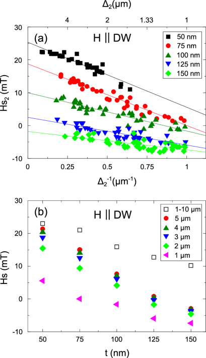
For relatively thin films, the energy difference between charged and uncharged magnetic domain walls is rather modest, giving rise to large spin rotations inside both domain walls and strong scaling of with . At the other end of the thickness spectrum, the width and energy of uncharged walls are mostly unchanged, whereas those of charged walls are significantly enhanced. The growing energy difference between the two types of domain walls leads to a reduction of with increasing CoFeB thickness. This scaling effect is most significant for wide a2 domains, since charged walls can attain their full width and energy without restrictions. For small , however, the domain walls are artificially confined to narrow domain stripes, leading to a finite-size reduction of the spin rotation within the walls and thus of their width and energy Franke et al. (2014). This effect hampers the reduction of with film thickness in narrow domains and, consequently, the scaling of with becomes less pronounced at the thick side of the CoFeB wedge. When the energy gain during charged-to-uncharged wall transformations exceeds the magnetic anisotropy energy of the domains, magnetic switching in the a2 domains can take place before zero applied magnetic field is reached. Negative switching fields are measured for narrow a2 domains and/or at large CoFeB film thicknesses, as shown in Figs. 7 (a) and (b).
The scaling behavior in our multiferroic heterostructure is qualitatively similar to that of two-dimensional magnetic systems with opposing interface and bulk anisotropies. In magnetic multilayers, for example, the interface anisotropy dominates the total energy of the system for very thin ferromagnetic films, but its contribution decays with thickness () as (see ref. Johnson et al. (1996)). This scaling effect causes a spin reorientation transition at a critical thickness . Exchange bias in ferromagnetic-antiferromagnetic bilayers is another well-known magnetic interface effect Nogués and Schuller (1999). The switching field in this case can also be negative (for one field sweep direction) and the magnitude of the exchange bias field scales as . In our system, the a2 domains are bordered by two straight and strongly pinned domain walls and the possible transformation of their internal spin structure acts as an interface-like potential energy. Consequently, the influence of the domain walls on diminishes with domain width as . Since the energy difference between charged and uncharged magnetic domain walls increases with ferromagnetic film thickness, both vertical and lateral scaling effects can be utilized to tailor micromagnetic switching effects in fully correlated multiferroic heterostructures.
V Conclusion
To conclude, we have investigated how magnetic domain wall pinning in a strain-coupled CoFeB/BaTiO3 heterostructure affects the magnetization reversal process. Depending on the in-plane field direction, two distinct mechanisms are identified. If magnetically charged domain walls with high energy are formed during a field sweep, the system lowers its energy via domain wall transformation into uncharged configurations, which corresponds to abrupt magnetic switching in every second stripe domain. This lateral modulation of magnetization reversal is unusual and can result in switching before zero applied magnetic field is reached. On the other hand, rotation of the applied magnetic field by 90∘ results in the formation of low-energy uncharged magnetic domain walls and a very different reversal behavior. In this configuration, all domains switch simultaneously to prevent the formation of high-energy charged magnetic domain walls. The magnetic switching event that is driven by domain wall transformations scales with the energy difference between the two types of magnetic walls and, thus, with the thickness of the CoFeB film. Also, since the local energy of the system varies with the density of magnetic domain walls, the switching field that is associated with domain wall transformations is inversely proportional to the domain width. The observed dependence of magnetization reversal on field direction is anticipated to be a general feature of continuous ferromagnetic films with a regular modulation of non-collinear magnetic anisotropy axes and a high density of pinned magnetic domain walls.
This work was supported by the Academy of Finland (Grant No. 260361), the European Research Council (ERC-2012-StG 307502- E-CONTROL) and the “Deutsche Forschungsgemeinschaft” via “Sonderforschungsbereich 668”.
References
- Labrune et al. (1989) M. Labrune, S. Andrieu, F. Rio, and P. Bernstein, J. Magn. Magn. Mater. 80, 211 (1989).
- Bruno et al. (1990) P. Bruno, G. Bayreuther, P. Beauvillain, C. Chappert, G. Lugert, D. Renard, J. P. Renard, and J. Seiden, J. Appl. Phys. 68, 5759 (1990).
- Lemerle et al. (1998) S. Lemerle, J. Ferré, C. Chappert, V. Mathet, T. Giamarchi, and P. L. Doussal, Phys. Rev. Lett. 80, 849 (1998).
- Chappert et al. (1998) C. Chappert, H. Bernas, J. Ferré, V. Kottler, J. P. Jamet, Y. Chen, E. Cambril, T. Devolder, F. Rousseaux, V. Mathet, et al., Science 280, 1919 (1998).
- Terris et al. (1999) B. D. Terris, L. Folks, D. Weller, J. E. E. Baglin, A. J. Kellock, H. Rothuizen, and P. Vettiger, Appl. Phys. Lett. 75, 403 (1999).
- Fassbender et al. (2004) J. Fassbender, D. Ravelosona, and Y. Samson, J. Phys. D: Appl. Phys. 37, R179 (2004).
- Fassbender and McCord (2008) J. Fassbender and J. McCord, J. Magn. Magn. Mater. 320, 579 (2008).
- Franken et al. (2012) J. H. Franken, H. J. M. Swagten, and B. Koopmans, Nat. Nanotechnol. 7, 499 (2012).
- Kim et al. (2012) S. Kim, S. Lee, J. Ko, J. Son, M. Kim, S. Kang, and J. Hong, Nat. Nanotechnol. 7, 567 (2012).
- Hamann et al. (2014) C. Hamann, R. Mattheis, I. Mönch, J. Fassbender, L. Schultz, and J. McCord, New J. Phys. 16, 023010 (2014).
- Bauer et al. (2013) U. Bauer, S. Emori, and G. S. D. Beach, Nat. Nanotechnol. 8, 411 (2013).
- Bauer et al. (2015) U. Bauer, L. Yao, A. J. Tan, P. Agrawal, S. Emori, H. L. Tuller, S. van Dijken, and G. S. D. Beach, Nat. Mater. 14, 174 (2015).
- Chu et al. (2008) Y.-H. Chu, L. W. Martin, M. B. Holcomb, M. Gajek, S.-J. Han, Q. He, N. Balke, C.-H. Yang, D. Lee, W. Hu, et al., Nature Mater. 7, 478 (2008).
- Lebeugle et al. (2009) D. Lebeugle, A. Mougin, M. Viret, D. Colson, and L. Ranno, Phys. Rev. Lett. 103, 257601 (2009).
- Heron et al. (2011) J. T. Heron, M. Trassin, K. Ashraf, M. Gajek, Q. He, S. Yang, D. E. Nikonov, Y.-H. Chu, S. Salahuddin, and R. Ramesh, Phys. Rev. Lett. 107, 217202 (2011).
- You et al. (2013) L. You, B. Wang, X. Zou, Z. S. Lim, Y. Zhou, H. Ding, L. Chen, and J. Wang, Phys. Rev. B 88, 184426 (2013).
- Lahtinen et al. (2011) T. H. E. Lahtinen, J. O. Tuomi, and S. van Dijken, Adv. Mater. 23, 3187 (2011).
- Lahtinen et al. (2012) T. H. E. Lahtinen, K. J. A. Franke, and S. van Dijken, Sci. Rep. 2, 258 (2012).
- Franke et al. (2012) K. J. A. Franke, T. H. E. Lahtinen, and S. van Dijken, Phys. Rev. B 85, 094423 (2012).
- Chopdekar et al. (2012) R. V. Chopdekar, V. K. Malik, A. F. Rodríguez, L. L. Guyader, Y. Takamura, A. Scholl, D. Stender, C. W. Schneider, C. Bernhard, F. Nolting, et al., Phys. Rev B 86, 014408 (2012).
- Streubel et al. (2013) R. Streubel, D. Köhler, R. Schäfer, and L. M. Eng, Phys. Rev. B 87, 054410 (2013).
- Franke et al. (2014) K. J. A. Franke, D. López González, S. J. Hämäläinen, and S. van Dijken, Phys. Rev. Lett. 112, 017201 (2014).
- Merz (1954) W. J. Merz, Phys. Rev. 95, 690 (1954).
- Hubert (1979) A. Hubert, IEEE Trans. Magn. 15, 1251 (1979).
- Hubert and Schäfer (1998) A. Hubert and R. Schäfer, Magnetic Domains. The Analysis of Magnetic Microstructures (Springer-Verlag, Berlin Heidelberg, 1998).
- Favieres et al. (2013) C. Favieres, J. Vergara, and V. Madurga, J. Phys.: Condens. Matter 25, 066002 (2013).
- Berger and Oepen (1992) A. Berger and H. P. Oepen, Phys. Rev. B 45, 12596(R) (1992).
- Frömter et al. (2011) R. Frömter, S. Hankemeier, H. P. Oepen, and J. Kirschner, Rev. Sci. Instrum. 82, 033704 (2011).
- Lilley (1950) B. Lilley, Philosophical Magazine and Journal of Science: Series 7 41, 792 (1950).
- Johnson et al. (1996) M. T. Johnson, P. J. H. Bloemen, F. J. A. den Broeder, and J. J. de Vries, Rep. Prog. Phys. 59, 1409 (1996).
- Nogués and Schuller (1999) J. Nogués and I. K. Schuller, J. Magn. Magn. Mater. 192, 203 (1999).