Resonant Visible Light Modulation with Graphene
Abstract
Fast modulation and switching of light at visible and near-infrared (vis-NIR) frequencies is of utmost importance for optical signal processing and sensing technologies. No fundamental limit appears to prevent us from designing wavelength-sized devices capable of controlling the light phase and intensity at gigaherts (and even terahertz) speeds in those spectral ranges. However, this problem remains largely unsolved, despite recent advances in the use of quantum wells and phase-change materials for that purpose. Here, we explore an alternative solution based upon the remarkable electro-optical properties of graphene. In particular, we predict unity-order changes in the transmission and absorption of vis-NIR light produced upon electrical doping of graphene sheets coupled to realistically engineered optical cavities. The light intensity is enhanced at the graphene plane, and so is its absorption, which can be switched and modulated via Pauli blocking through varying the level of doping. Specifically, we explore dielectric planar cavities operating under either tunneling or Fabry-Perot resonant transmission conditions, as well as Mie modes in silicon nanospheres and lattice resonances in metal particle arrays. Our simulations reveal absolute variations in transmission exceeding as well as an extinction ratio dB with small insertion losses using feasible material parameters, thus supporting the application of graphene in fast electro-optics at vis-NIR frequencies.
I INTRODUCTION
Graphene –the two-dimensional (2D) honeycomb lattice of carbon atoms– exhibits extraordinary optoelectronic properties derived from its peculiar band structure of massless charge carriers Castro Neto et al. (2009). Notably, its optical absorption can be switched on/off via electrical doping. In its undoped state it absorbs a fraction of the incident light Nair et al. (2008); Mak et al. (2008) over a broad spectral range within the vis-NIR as a result of direct electron-hole pair transitions between its lower occupied Dirac cones and the upper unoccupied cones (two inequivalent ones in every Brillouin zone Wallace (1947); Castro Neto et al. (2009)). In contrast, when electrically doped, an optical gap is opened that suppresses vertical optical transitions for photon energies below , where is the change in Fermi energy relative to the undoped state (see Fig. 1a). In practice, values of as high as 1 eV can be obtained through electrical gating Chen et al. (2011), therefore enabling the modulation of light absorption down to the visible regime. Chemical methods permit achieving even higher levels of doping Khrapach et al. (2012), which could be combined with additional electrostatically induced variations of around a high bias point to reach control over shorter light wavelengths.
Fast light modulation at vis-NIR frequencies can find application in optical signal processing and interconnect switching, where there is a great demand for integrated wavelength-sized devices capable of operating at terahertz commutation rates. The extraordinary electro-optical response of graphene provides a key ingredient for the realization of these types of devices. However, the exploitation of atomically thin carbon films for light modulation faces the problem of their relatively weak interaction with light. A possible solution to enhance this interaction is to use the intrinsic plasmons that show up in the optical gap of this material when it is highly doped Vakil and Engheta (2011); Koppens et al. (2011); Nikitin et al. (2011); Ju et al. (2011); Fei et al. (2011); Bludov et al. (2012); Chen et al. (2012); Fei et al. (2012); Fang et al. (2013); Brar et al. (2013); Fang et al. (2014a); Jang et al. (2014); García de Abajo (2014). Resonant coupling to graphene plasmons can even result in complete optical absorption Thongrattanasiri et al. (2012), as exemplified by the observation of large tunable light modulation at mid-IR frequencies in periodically nanostructured graphene Fang et al. (2014a); Jang et al. (2014). The extension of this strategy down to the vis-NIR spectral domain remains a challenge, as it requires to laterally pattern the carbon film with nm features, which are currently unattainable through conventional lithographies, although chemical self-assembly might offer a viable way of producing the required structures Müllen (2014).
An alternative solution consists in amplifying the absorption of undoped graphene either by increasing the region over which light interacts with it or by coupling the carbon film to an optical cavity of high quality factor (i.e., by trapping light during long times near the graphene). A broadband modulator has been demonstrated with the former approach by exposing a long path of an optical waveguide to electrically gated graphene Liu et al. (2011). Additionally, coupling to photonic cavities has been explored using plasmonic structures, photonic-crystals, and metamaterials Emani et al. (2012); Gan et al. (2012); Yao et al. (2013); Li and Yua (2013); Mousavi et al. (2013); T. Stauber et al. (2014); Emani et al. (2014). For example, monolayer graphene integrated with metallic metasurfaces has been used to control the optical response (resonance position, depth, and linewidth) at mid-IR frequencies Yao et al. (2013); Li and Yua (2013); Mousavi et al. (2013); Emani et al. (2014). Similarly, large intensity modulations () of mid-IR light over a nm bandwidth have been reported in graphene-loaded plasmonic antennas (Yao et al., 2013). Additionally, a resonance wavelength shift nm accompanied by a 4-fold variation in reflectivity has been observed in the NIR by coupling graphene to a photonic crystal cavity Gan et al. (2012); Majumdar et al. (2013). Enhanced visible light absorption in graphene has also been demonstrated (without modulation) by combining monolayer graphene with metamaterials Papasimakis et al. (2010), gold nanovoid arrays Zhu et al. (2013), and photonic waveguides Piper and Fan (2014), as well as by coupling multilayer graphene under total internal reflection Pirruccio et al. (2013).
In this work, we study four different mechanisms that produce resonant enhancement in the absorption of undoped graphene over the vis-NIR spectral domain, thus serving as optical modulators with large depth in that frequency range. Specifically, we focus on the coupling of graphene to (1) resonant tunneling transmission cavities, (2) resonant Fabry-Perot cavities, (3) Mie modes of silicon spheres, and (4) lattice resonances in periodic particle arrays, which we investigate by calculating reflection, transmission, and absorption spectra of structures containing either doped or undoped graphene films. We predict modulation depths in vis-NIR light transmission exceeding , with small insertion losses, thus revealing the potential of graphene for fast electro-optics within such a technologically important range of optical frequencies.
II RESULTS AND DISCUSSION
II.1 Graphene optical switch based upon resonant tunneling transmission
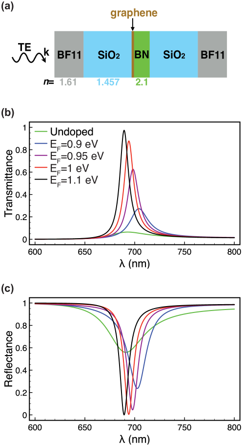
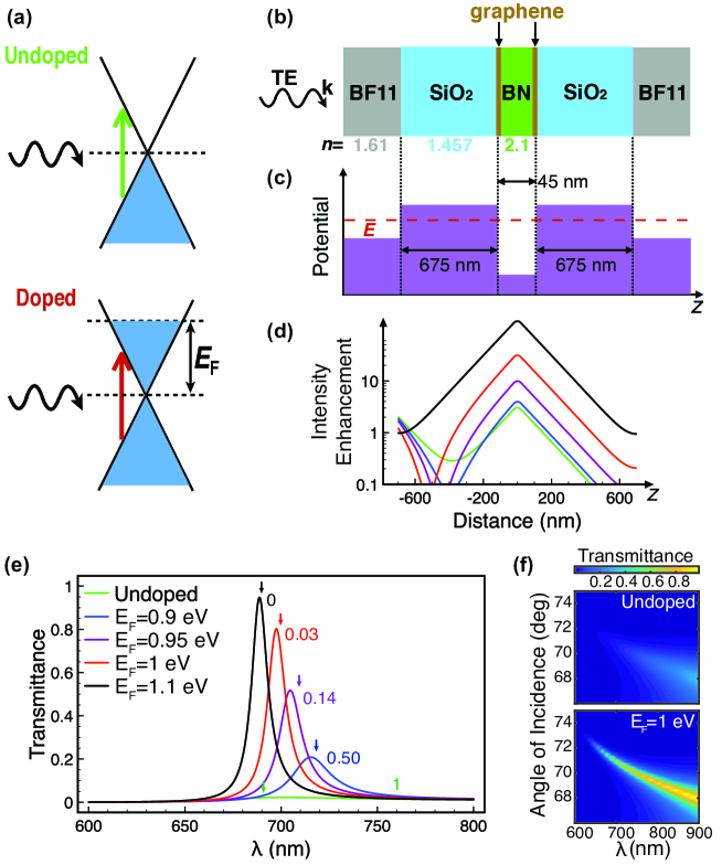
We illustrate the concept of resonant switching and modulation of graphene absorption by coupling to a high-quality-factor planar cavity. In particular, we consider the multilayer structure depicted in Fig. 1b, consisting of a high-refractive-index BN planar waveguide () flanked by low-index silica spacers (). The waveguide hosts guided modes that can be resonantly coupled to light of well-defined parallel wave vector (i.e., for a collimated incident beam). In our case, light is incident from the left under total internal reflection conditions at the BF11-SiO2 interface (). The evanescent spill out of light intensity penetrating inside the left silica spacer can reach the BN waveguide, where it is amplified to further extend towards the rightmost interface. In the absence of absorption, full transmission can always be achieved at a resonant wavelength that depends on incidence angle. This phenomenon, known as resonant tunneling transmission, was previously explored with electron waves Chang et al. (1974). There is complete analogy between TE light propagation in the planar structure under consideration and the evolution of an electron according to Schrödinger equation Sainidou et al. (2010) (see Methods). The equivalent electron has energy and evolves along a potential profile as shown in Fig. 1c. The latter is directly related to the refractive index, with higher index corresponding to lower values of the potential. The presence of a bound state is always guaranteed in a 1D cavity, and so is the existence of a full transmission resonance when this bound state lies inside the potential barrier Chang et al. (1974). Under complete-transmission conditions, the intensity has to decay exponentially from the waveguide to the far medium (i.e., across the rightmost silica barrier), to reach the same value as the incident intensity, so that the near field has to be strongly amplified at the central waveguide. This type of enhancement, which is clearly illustrated in Fig. 1d, has been experimentally corroborated by measuring a -fold increase in the fluorescence from quantum dots placed near the central waveguide under resonance conditions in a structure similar to the one considered here Sainidou et al. (2010). This effect can find application to sensing, for example by replacing the waveguide by a high-index fluid with dispersed analytes in it. Instead, in this article we use the resonant tunneling transmission concept to amplify the effect of absorption taking place at the graphene.
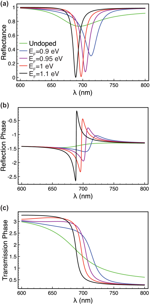
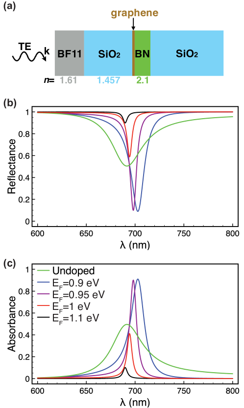
The structure under consideration (Fig. 1b) contains a graphene film on either side of the central BN waveguide. Besides its high index of refraction, the choice of BN for the central waveguide is convenient because this combination of materials is compatible with high-quality graphene Dean et al. (2010), which can be realistically described with the models for the conductivity discussed in the Methods section. Nevertheless, we assume a conservative value of the graphene mobility throughout this work, cmV s. When the carbon layer is highly doped (eV), it becomes nearly lossless (i.e., small ) at the waveguide resonance wavelength, so that the peak transmission reaches (Fig. 1e) and the light intensity enhancement at the waveguide exceeds a factor of 140. In contrast, in the undoped state, the carbon layer becomes lossy (i.e., nearly real ), so the enhancement is strongly suppressed, and the transmission drops to very small values. The extinction ratio (i.e., the ratio of transmissions in doped and undoped states) is dB. The transmission can be in fact tuned continuously between these two extreme values by varying the level of doping (see Fig. 1e). The decrease in transmission produced when moving from highly doped to undoped graphene is due to both absorption and reflection, as the local change in the response of the carbon layer produces a departure from the conditions of resonant tunneling. Actually, reflection accounts for the bulk of the depletion in transmission, as shown in the supplementary Fig. 6. This can be exploited to simplify the structure, which still undergoes unity-order modulation of the reflection upon graphene doping after removing the rightmost BF11 out-coupling medium (see supplementary Fig. 8). Even more, only a single graphene layer is needed to modulate the structure (see supplementary Fig. 7).
The wavelength of operation of this modulator is essentially determined by the waveguide mode, as coupling to the BF11 media is just producing a slight shift. Understandably, the reflection minimum is observed to be only mildly modified when the rightmost glass is removed (cf. supplementary Figs. 7 and 8). Then, we find it useful to derive a simple analytical expression for the variation of the waveguide resonance wavelength (see Eq. (2) in the Methods section), in which the graphene conductivity enters to first order as . The role of the real and imaginary parts of is thus clearly established: the former determines the depth of the modulation, whereas is responsible for the resonance shift. The resonance wavelengths given by Eq. (2) are indicated by downwards arrows in Fig. 1e, in excellent agreement with the observed transmission maxima. Notice the initial redshift with increasing doping, followed by a blueshift back to the original position in the perfectly transmitting structure, which essentially mimics the evolution of with doping.
Obviously, the resonance wavelength also depends on the angle of incidence and it can be pushed down to the visible regime (Fig. 1f), although the maximum transmission decreases towards smaller wavelengths due to the gradual involvement of interband transitions in the graphene.
In a realistic device, the two graphene layers of Fig. 1b could be biased with a relative potential difference , so that they will reach a Fermi energy , where m/s is the Fermi velocity in the carbon layer, while and are the static permittivity and thickness of the BN layer. For nm, a value of eV is obtained with potentials V. For the single graphene-layer structures noted above (see supplementary Figs. 7 and 8), doping could be introduced through the addition of a transparent electrode.
II.2 Graphene optical switch based upon a Fabry-Perot resonator
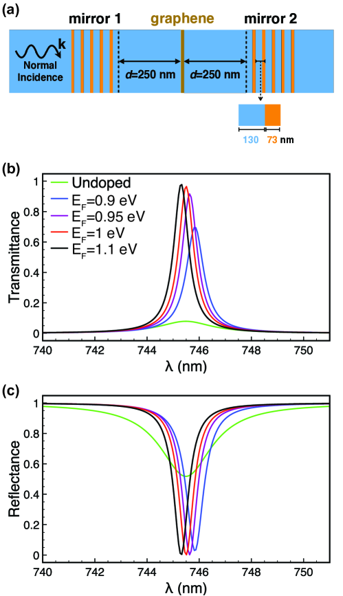
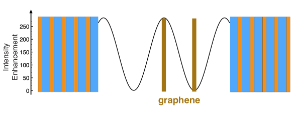
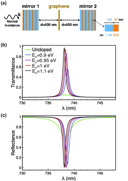
The concept of the tunneling structure in Fig. 1 can be extrapolated to other types of resonators in which the incident field also undergoes a large enhancement at a position decorated with graphene. A particularly convenient implementation of this idea is presented in Fig. 2, as it allows operating under normal incidence conditions. More precisely, we replace the tunneling structure by a Fabry-Perot (FP) frequency-selective filter, consisting of a cavity flanked by two non-absorbing, nearly perfectly reflecting mirrors. In practical devices, one generally uses Bragg mirrors such as those sketched in Fig. 2a, which are easy to fabricate by multilayer deposition. We consider a separation between the FP mirrors that produces a single resonant transmission peak in the nm spectral region. At resonance, light is trapped inside the cavity, so it makes many passes through it before escaping, thus generating a large field enhancement at several interference nodes. We place the graphene at one of those nodes. A similar strategy has been recently followed for all-optical nonlinear NIR light modulation Fang et al. (2014b). An interplay between absorption (imaginary part of the susceptibility) and polarization (real part) in the graphene is then taking place, leading to large (but not totally complementary) modulations in reflection and transmission, similar to those discussed above for the tunneling device. Incidentally, similar performance is obtained by filling the cavity with glass and reducing its size (see supplementary Fig. 9), thus configuring a more robust structure. We have also verified (results not shown) that further reduction of the cavity leads to a 1D photonic crystal that exhibits a normal-incidence gap, in which a localized optical mode exists due to the addition of an impurity (i.e., the cavity itself); the graphene can then couple to this localized mode to produce an even more compact light modulator. We find it interesting that the cavity is unaffected if the graphene is placed at an antinode of the interference standing wave inside the cavity (see supplementary Fig. 10), as this opens the possibility of using an optically inactive graphene layer located at an antinode and serving as a gate with which to dope the other graphene layer placed at a node.
II.3 Enhanced graphene optical absorption and switching by coupling to Mie cavities
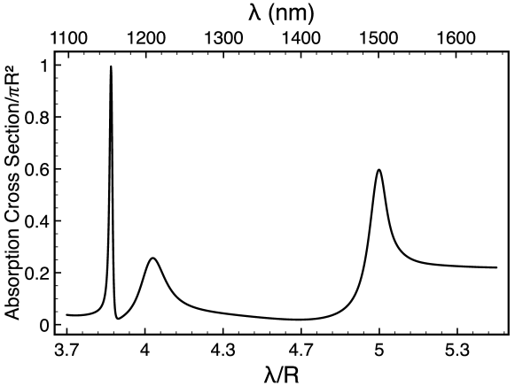
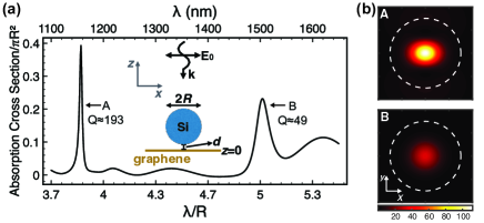
Figure 3a represents the change in the absorption cross section undergone by a layer of undoped graphene when we place a silicon sphere () in its vicinity. These types of silicon colloids have been recently synthesized and used as excellent photonic cavities Garin et al. (2014). The increase in absorption cross section remains a small fraction of the extinction produced by the sphere in this configuration (e.g., 6.1% and 2.7% for the Mie modes labeled A and B in Fig. 3a), so we approximate it as
| (1) |
where is the parallel component of the electric field scattered by the sphere alone, is the incident field, and we integrate over the graphene plane. The field is obtained from Mie theory Mie (1908). This approximate method yields similar results as the change in elastic (dark-field) scattering due to doping, calculated from a rigorous modal expansion for the sphere-graphene system (see supplementary Fig. 11). In Fig. 3 the cross section is normalized to the projected area of the sphere and the wavelength is normalized to the sphere radius , so that this plot is independent of , apart from the relatively small variations of the permittivity of silicon over the NIR. Despite the subwavelength size of the particle, its high allows it to trap light within Mie modes of high quality factor ( and in modes A and B, see Fig. 3a), giving rise to large local enhancements of the near-field intensity at the plane of the graphene (see Fig. 3b). This in turn boots the absorption, which takes remarkably large values, with a peak increase in cross section reaching of the projected area of the sphere. Interestingly, the spatial distribution of absorption (proportional to the intensity plotted in Fig. 3b) is strongly confined to the near-contact region, which could be exploited for engineering the spatial distribution of optically induced heat deposition, as well as for controlling the graphene electron-gas ultrafast dynamics before relaxation and thermalization of the absorbed energy takes place.
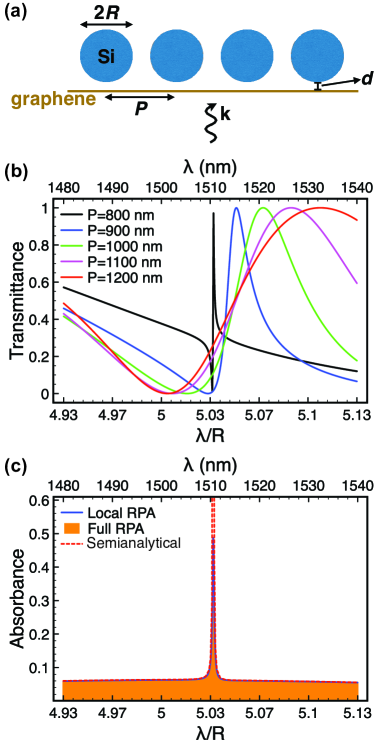
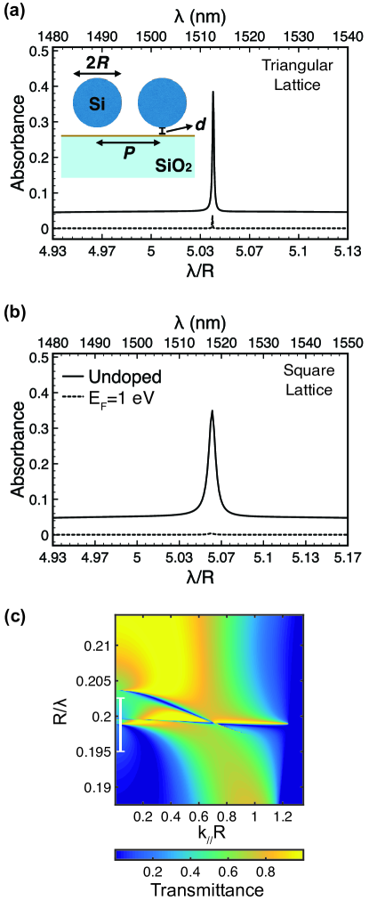
Because the maximum value of produced by a single silicon sphere is comparable to its projected area, we expect to obtain unity-order changes in the absorption when the graphene is decorated by a periodic array. This is illustrated in Fig. 4, where we concentrate on the spectral region around the rightmost Mie mode of Fig. 3a (labeled B). We consider the silicon spheres to be arranged in a triangular lattice, which we simulate using a layer-KKR approach Stefanou et al. (2000) (see Methods). Interestingly, there is strong interaction between the particles for the lattice spacings under consideration, which can be intuitively quantified from the fact that the extinction cross section of the sphere equals the area of a circle of diameter m. The transmission of the particle array experiences dramatic spectral variations as is changed, eventually generating a narrow transmission peak, which is relatively close, but not on top of the lowest-order Wood anomaly, occurring when the wavelength is equal to the period at normal incidence; we thus attribute this feature to the interaction between Mie modes of the spheres, as the wavelength is close (but not right on) a lattice resonance that narrows the resulting spectral feature (see supplementary Fig. 12). A similar mechanism leading to sharp, narrow asymmetric resonances has already been described in the context of cavity-waveguide coupling Fan (2002). The absorbance associated with this narrow peak is boosted, approaching 50% with undoped graphene (Fig. 4c), whereas doped graphene shows comparatively negligible absorbance (not shown).
In the layer-KKR simulation method Stefanou et al. (2000), the homogeneous graphene film enters through its reflection and transmission coefficients for different diffracted orders (i.e., a collection of propagating and evanescent plane waves, each of them corresponding to a fixed value of the parallel wave vector). This allows us to use the full random-phase approximation (RPA) conductivity Wunsch et al. (2006); Hwang and Das Sarma (2007) , which includes nonlocal effects associated with finite parallel wave vectors corresponding to those diffracted orders. Because the size of the spheres and the lattice periods under consideration are large compared with (i.e., the ratio of the graphene Fermi velocity to the light frequency, nm for a wavelength of m), nonlocal effects are in fact negligible, which explains why we obtain the same results on the scale of the figure by just using the value for the conductivity in undoped graphene instead of the full RPA. The same argument explains why plasmons are not excited here in doped graphene. Additionally, we obtain very similar results with the semi-analytical model of Eq. (1) (except very close to the resonance), which we apply by averaging the parallel electric-field intensity enhancement over a unit cell. The intensity in the semi-analytical model is calculated without the graphene, just to provide insight into the absorption process. However, when we calculate it including the carbon layer, the absorbance predicted by Eq. (1) cannot be told apart on the scale of the figure from the one given by the far-field transmittance and reflectance (i.e., ), thus corroborating the numerical accuracy of our calculations.
For tutorial purposes, the above discussion on the coupling to Mie resonances is based on self-standing graphene, but qualitatively similar conclusions are obtained when examining graphene supported on a glass substrate (see supplementary Fig. 12).
II.4 Enhanced graphene optical absorption and switching by coupling to lattice resonances
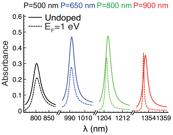
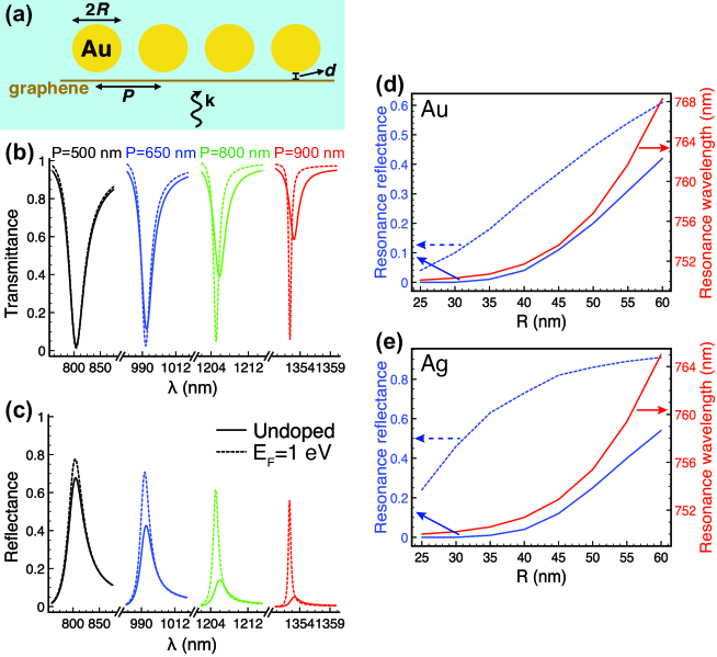
We now discuss the absorption enhancement produced by lattice resonances, for which strong scatterers such as metallic particles are preferable. Although metals introduce additional losses, their absorbance is relatively small in the NIR, so graphene can still make a big difference. This is corroborated in Fig. 5, where we consider a graphene layer decorated with a 2D square array of gold spheres surrounded by silica for different values of the lattice spacing . The transmission (Fig. 5b) and reflection (Fig. 5c) spectra of these structures exhibit sharp features emerging near the Wood anomaly condition (i.e., when the wavelength in the surrounding dielectric is close to the period, or equivalently, when a diffraction order becomes grazing), which can be easily understood in terms of lattice resonances Lord Rayleigh (1907); García de Abajo (2007). As the period is increased, these features move to the red, where the metal is less lossy, and consequentally, the resonances become narrower. The additional absorption produced by the undoped graphene then becomes more noticeable (see supplementary Fig. 13), eventually causing a decrease in peak transmittance of , accompanied by a 28-fold reduction in reflectance.
III CONCLUSIONS AND OUTLOOK
In conclusion, monolayer graphene can be used to produce unity-order changes in the transmission, reflection, and absorption of light down to the vis-NIR domain when comparing its electrically doped and undoped states, considering realistic levels of doping (eV) that are currently attainable through electrical gating. It should be emphasized that the calculations here presented for geometries containing only graphene and dielectrics are scalable, so that the main requirement is that the graphene can be switched back and forth between and , where is the photon energy under operation; provided this condition is satisfied, all geometrical lengths and the light wavelength can be scaled by a common factor, leading to the same values for the transmission and absorption. For example, the modulation at 700 nm wavelength predicted in Fig. 1 with doping up to eV can be also extrapolated to the 1550 nm telecom wavelength with doping up to eV after scaling all lengths by a factor of .
Interestingly, we find that undecorated graphene in a planar multilayer dielectric structure can modulate transmission near the point of resonant tunneling under total internal reflection, with absolute changes exceeding and an extinction ratio dB. Similar levels of modulation are found for graphene placed inside a realistic Fabry-Perot cavity. Large vis-NIR modulation depths are also predicted in a graphene layer decorated with periodic arrays of silicon or gold particles. Obviously, the depth of modulation is reduced by coupling to impurities in low-quality graphene, where optical losses can be still significant under high doping. Nonetheless, we find a substantial degree of modulation even in the presence of large residual absorption (e.g., modulation in the device of Fig. 1 when the residual optical loss amounts to 14% of the ideal absorption-free highly doped material, as shown in Fig. 1e).
The mechanisms here considered for light modulation by graphene can be integrated in devices spanning only a few square microns in size, so they require a relatively small amount of doping charge to operate. We thus anticipate that these systems will be able to modulate vis-NIR light at high speeds with a minute consumption of power, typical of capacitive devices. This is an advantage with respect to alternative commutation devices based on quantum-wells Inoue et al. (2014) and phase-change materials Wen et al. (2015). For example, we envision an integrated commutation device operating over an area m2 (i.e., covering a customary optical beam size), for which we estimate a capacitance pF, where we consider (DC silica) and a gate separation nm (notice that there is great flexibility in the choice of in some of our devices). The time response is then limited by the sheet resistance of the graphene layer (), giving an overall cutoff frequency for the electrical bandwidth of GHz, while the optical limit for the electrical modulation of the photonic response (i.e., the effect related to the decay time of the resonance) renders a larger cutoff (GHz for a cavity length m and a quality factor ). The large electro-optical response of graphene combined with its small volume are thus ideal attributes for the design of fast optical modulators and switches operating in the vis-NIR, which can benefit from the coupling to optical resonators such as those explored in the present work. In particular, the planar structures presented in Figs. 1 and 2, which rely on unstructured graphene, provide relatively affordable designs that are appealing for micro integration and mass production.
METHODS
Schrödinger equation for TE polarized light in a planar multilayer structure. For our purpose, it is convenient to write the wave equation for the electric field as , where is the free-space light wave vector and is the frequency and position dependent local dielectric function. We consider a structure formed by several planar layers (see Fig. 1), illuminated under TE polarization (i.e., with the electric field parallel to the planes), and oriented with the axis perpendicular to the interfaces, so that the spatial dependence of the dielectric function is only through (i.e., ). Then, we can write the electric field as , where is the parallel wave vector component, which is determined by the angle of incidence at the near medium of permittivity . With this form of the electric field, the wave equation reduces to
where we have defined the equivalent potential and the effective energy . Interestingly, metals () and dielectrics () produce repulsive () and attractive () potentials, respectively, in this equivalent Schrödinger model.
Graphene conductivity. We model graphene through its 2D conductivity. For doped graphene, we use a previously reported local-RPA model Falkovsky and Varlamov (2007); Falkovsky and Pershoguba (2007), conveniently corrected to account for finite temperature in both intra- and interband transitions García de Abajo (2014). More precisely,
where is the Fermi energy,
effectively accounts for thermal corrections in the doping level, and is the Fermi-Dirac distribution function. For undoped graphene, the above expression converges to the well-known limit . We further account for finite wave-vector effects (nonlocality) through the full-RPA model Wunsch et al. (2006); Hwang and Das Sarma (2007), in which depends on and , but we find those effects to be negligible (see Fig. 4), as expected from the large mismatch between the Landau damping range at vis-NIR frequencies and both the light wavelength and the distances involved in the structures under consideration. Throughout this work, we take K and assume an inelastic decay time given by the Drude model Ashcroft and Mermin (1976); Jablan et al. (2009) (i.e., ) with an impurity limited DC mobility cmV s.
Multilayer structure simulation. The transmission and field enhancement of planar multilayers are obtained through a standard transfer matrix approach. In particular, we use the reflection and transmission coefficients for a plane wave of parallel wave vector incident from medium 1 on a graphene layer of conductivity placed at the interface with another medium 2, which upon direct solution of Maxwell’s equations for the (TE) polarization under consideration are found to be Jackson (1999) and , respectively, where and . For completeness, we give the coefficients for (TM) polarization: and , where . Incidentally, the sign of the square root is chosen to yield positive real values. These expressions also describe the coefficients of interfaces without graphene, simply by taking .
For tunneling transmission (Fig. 1), the resonant wavelength of maximum transmission is only slightly changed from the central waveguide Fabry-Perot resonance condition, , where is the waveguide thickness, ( under the conditions of this work) is the order of the resonance, and (we choose media 1 and 2 right outside and inside the waveguide, respectively). To linear order in , we find
| (2) |
Incidentally, has units of velocity in CGS, so this expression is dimensionally correct.
Particle arrays. We use the layer-KKR method to simulate periodic particle arrays near planar interfaces Stefanou et al. (2000). This method relies on an expansion of the electromagnetic field in terms of spherical vector waves around the particles and plane waves near the graphene. The scattering by the spheres then involves multiplication by Mie coefficients, whereas the graphene enters through its reflection coefficients (see above). Plane and spherical waves are analytically transformed into each other, giving rise to a self-consistent system of equations projected on the coefficients of the sphere multipoles. Translational lattice symmetry is used to reduce the number of plane waves to those of a discrete set corresponding to different diffraction orders (i.e., two waves of orthogonal polarizations for each reciprocal lattice vector). We achieve convergence with such waves and neglecting sphere multipoles of orbital angular momentum number above 7. This method directly yields the reflection, transmission, and absorption coefficients used to produce Figs. 4 and 5 for periodic particle arrays near planar interfaces including graphene.
Acknowledgement
This work has been supported in part by the European Commission (contract Nos. Graphene Flagship CNECT-ICT-604391 and FP7-ICT-2013-613024-GRASP) and the "Fondo Europeo de Desarrollo Regional" (FEDER, contract No. TEC2013-46168-R).
References
- Castro Neto et al. (2009) A. H. Castro Neto, F. Guinea, N. M. R. Peres, K. S. Novoselov, and A. K. Geim, Rev. Mod. Phys. 81, 109 (2009).
- Nair et al. (2008) R. R. Nair, P. Blake, A. N. Grigorenko, K. S. Novoselov, T. J. Booth, T. Stauber, N. M. R. Peres, and A. K. Geim, Science 320, 1308 (2008).
- Mak et al. (2008) K. F. Mak, M. Y. Sfeir, Y. Wu, C. H. Lui, J. A. Misewich, and T. F. Heinz, Phys. Rev. Lett. 101, 196405 (2008).
- Wallace (1947) P. R. Wallace, Phys. Rev. 71, 622 (1947).
- Chen et al. (2011) C. F. Chen, C. H. Park, B. W. Boudouris, J. Horng, B. Geng, C. Girit, A. Zettl, M. F. Crommie, R. A. Segalman, S. G. Louie, et al., Nature 471, 617 (2011).
- Khrapach et al. (2012) I. Khrapach, F. Withers, T. H. Bointon, D. K. Polyushkin, W. L. Barnes, S. Russo, M. F. Craciun, and F. Monica, Adv. Mater. 24, 2844 (2012).
- Vakil and Engheta (2011) A. Vakil and N. Engheta, Science 332, 1291 (2011).
- Koppens et al. (2011) F. H. L. Koppens, D. E. Chang, and F. J. García de Abajo, Nano Lett. 11, 3370 (2011).
- Nikitin et al. (2011) A. Y. Nikitin, F. Guinea, F. J. García-Vidal, and L. Martín-Moreno, Phys. Rev. B 84, 161407(R) (2011).
- Ju et al. (2011) L. Ju, B. Geng, J. Horng, C. Girit, M. Martin, Z. Hao, H. A. Bechtel, X. Liang, A. Zettl, Y. R. Shen, et al., Nat. Nanotech. 6, 630 (2011).
- Fei et al. (2011) Z. Fei, G. O. Andreev, W. Bao, L. M. Zhang, A. S. McLeod, C. Wang, M. K. Stewart, Z. Zhao, G. Dominguez, M. Thiemens, et al., Nano Lett. 11, 4701 (2011).
- Bludov et al. (2012) Y. V. Bludov, N. M. R. Peres, and M. I. Vasilevskiy, Phys. Rev. B 85, 245409 (2012).
- Chen et al. (2012) J. Chen, M. Badioli, P. Alonso-González, S. Thongrattanasiri, F. Huth, J. Osmond, M. Spasenović, A. Centeno, A. Pesquera, P. Godignon, et al., Nature 487, 77 (2012).
- Fei et al. (2012) Z. Fei, A. S. Rodin, G. O. Andreev, W. Bao, A. S. McLeod, M. Wagner, L. M. Zhang, Z. Zhao, M. Thiemens, G. Dominguez, et al., Nature 487, 82 (2012).
- Fang et al. (2013) Z. Fang, S. Thongrattanasiri, A. Schlather, Z. Liu, L. Ma, Y. Wang, P. M. Ajayan, P. Nordlander, N. J. Halas, and F. J. García de Abajo, ACS Nano 7, 2388 (2013).
- Brar et al. (2013) V. W. Brar, M. S. Jang, M. Sherrott, J. J. Lopez, and H. A. Atwater, Nano Lett. 13, 2541 (2013).
- Fang et al. (2014a) Z. Fang, Y. Wang, A. Schlather, Z. Liu, P. M. Ajayan, F. J. García de Abajo, P. Nordlander, X. Zhu, and N. J. Halas, Nano Lett. 14, 299 (2014a).
- Jang et al. (2014) M. S. Jang, V. W. Brar, M. C. Sherrott, J. J. Lopez, L. Kim, S. Kim, M. Choi, and H. A. Atwater, Phys. Rev. B 90, 165409 (2014).
- García de Abajo (2014) F. J. García de Abajo, ACS Photon. 1, 135 (2014).
- Thongrattanasiri et al. (2012) S. Thongrattanasiri, F. H. L. Koppens, and F. J. García de Abajo, Phys. Rev. Lett. 108, 047401 (2012).
- Müllen (2014) K. Müllen, ACS Nano 8, 6531 (2014).
- Liu et al. (2011) M. Liu, X. Yin, E. Ulin-Avila, B. Geng, T. Zentgraf, L. Ju, F. Wang, and X. Zhang, Nature 474, 64 (2011).
- Emani et al. (2012) N. K. Emani, T.-F. Chung, X. Ni, A. V. Kildishev, Y. P. Chen, and A. Boltasseva, Nano Lett. 12, 5202 (2012).
- Gan et al. (2012) X. Gan, K. F. Mak, Y. Gao, Y. You, F. Hatami, J. Hone, T. F. Heinz, and D. Englund, Nano Lett. 12, 5626 (2012).
- Yao et al. (2013) Y. Yao, M. A. Kats, P. Genevet, N. Yu, Y. Song, J. Kong, and F. Capasso, Nano Lett. 13, 1257 (2013).
- Li and Yua (2013) Z. Li and N. Yua, Appl. Phys. Lett. 102, 131108 (2013).
- Mousavi et al. (2013) S. H. Mousavi, I. Kholmanov, K. B. Alici, D. Purtseladze, N. Arju, K. Tatar, D. Y. Fozdar, J. W. Suk, Y. Hao, A. B. Khanikaev, et al., Nano Lett. 13, 1111 (2013).
- T. Stauber et al. (2014) G. G. T. Stauber, , and F. J. García de Abajo, Phys. Rev. Lett. 112, 077401 (2014).
- Emani et al. (2014) N. K. Emani, T.-F. Chung, A. V. Kildishev, V. M. Shalaev, Y. P. Chen, and A. Boltasseva, Nano Lett. 14, 78 (2014).
- Majumdar et al. (2013) A. Majumdar, J. Kim, J. Vuckovic, and F. Wang, Nano Lett. 13, 515 (2013).
- Papasimakis et al. (2010) N. Papasimakis, Z. Luo, Z. X. Shen, F. De Angelis, E. Di Fabrizio, A. E. Nikolaenko, and N. I. Zheludev, Opt. Express 18, 8353 (2010).
- Zhu et al. (2013) X. Zhu, L. Shi, M. S. Schmidt, A. Boisen, O. Hansen, J. Zi, S. Xiao, and N. A. Mortensen, Nano Lett. 13, 4690 (2013).
- Piper and Fan (2014) J. R. Piper and S. Fan, ACS Photon. 1, 347 (2014).
- Pirruccio et al. (2013) G. Pirruccio, L. Martín Moreno, G. Lozano, and J. Gómez Rivas, ACS Nano 7, 4810 (2013).
- Chang et al. (1974) L. L. Chang, L. Esaki, and R. Tsu, Appl. Phys. Lett. 24, 593 (1974).
- Sainidou et al. (2010) R. Sainidou, J. Renger, T. V. Teperik, M. U. González, R. Quidant, and F. J. García de Abajo, Nano Lett. 10, 4450 (2010).
- Dean et al. (2010) C. R. Dean, A. F. Young, I. Meric, C. Lee, L. Wang, S. Sorgenfrei, K. Watanabe, T. Taniguchi, P. Kim, K. L. Shepard, et al., Nat. Nanotech. 5, 722 (2010).
- Fang et al. (2014b) L. Fang, A. Madouri, A. Cavanna, I. Sagnes, D. Chouteau, X. Lafosse, G. Beaudoin, and J.-L. Oudar, in 26th Int. Conf. on Indium Phosphide and Related Materials (2014b), pp. 978–1–4799–5729–3.
- Garin et al. (2014) M. Garin, R. Fenollosa, R. Alcubilla, L. Shi, L. F. Marsal, and F. Meseguer, Nat. Commun. 5, 3440 (2014).
- Mie (1908) G. Mie, Ann. Phys. (Leipzig) 25, 377 (1908).
- Wunsch et al. (2006) B. Wunsch, T. Stauber, F. Sols, and F. Guinea, New J. Phys. 8, 318 (2006).
- Hwang and Das Sarma (2007) E. H. Hwang and S. Das Sarma, Phys. Rev. B 75, 205418 (2007).
- Stefanou et al. (2000) N. Stefanou, V. Yannopapas, and A. Modinos, Comput. Phys. Commun. 132, 189 (2000).
- Fan (2002) S. Fan, Appl. Phys. Lett. 80, 908 (2002).
- Lord Rayleigh (1907) Lord Rayleigh, Philos. Mag. 14, 60 (1907).
- García de Abajo (2007) F. J. García de Abajo, Rev. Mod. Phys. 79, 1267 (2007).
- Inoue et al. (2014) T. Inoue, M. De Zoysa, T. Asano, and S. Noda, Nat. Mater. 13, 928 (2014).
- Wen et al. (2015) S.-C. Wen, C.-W. Chang, C.-M. Lin, H. an Liu, V. K. Hsiao, J. Yu, and Z. Chen, Opt. Commun. 334, 110 (2015).
- Falkovsky and Varlamov (2007) L. A. Falkovsky and A. A. Varlamov, Eur. Phys. J. B 56, 281 (2007).
- Falkovsky and Pershoguba (2007) L. A. Falkovsky and S. S. Pershoguba, Phys. Rev. B 76, 153410 (2007).
- Ashcroft and Mermin (1976) N. W. Ashcroft and N. D. Mermin, Solid State Physics (Harcourt College Publishers, New York, 1976).
- Jablan et al. (2009) M. Jablan, H. Buljan, and M. Soljačić, Phys. Rev. B 80, 245435 (2009).
- Jackson (1999) J. D. Jackson, Classical Electrodynamics (Wiley, New York, 1999).
- Kühler et al. (2012) P. Kühler, F. J. García de Abajo, P. Leiprecht, A. Kolloch, J. Solis, P. Leiderer, and J. Siegel, Opt. Express 20, 22063 (2012).
