Doping Asymmetry of a 3-orbital CuO2 Hubbard Model
Abstract
While both the hole and electron doped cuprates can exhibit -wave superconductivity, the local distribution of the doped carriers is known to be significantly different with the doped holes going primarily on the O sites while the doped electrons go on the Cu sites. Here we report the results of density-matrix-renormalization-group calculations for a three-orbital model of a CuO2 lattice. In addition to the asymmetric dependence of the intra-unit-cell occupation of the Cu and O for hole and electron doping, we find important differences in the longer range spin and charge correlations. As expected, the pair-field response has a -like structure for both the hole and electron doped systems.
How well does a 3-orbital Hubbard model describe the properties of the cuprates? These materials are known to be charge-transfer systems and from the analysis of Zaanan, Sawatzky and Allen ref:1 one would expect that a minimal model which includes a Cu 3 orbital and two O 2 orbitals per unit cell would be required. Indeed, early on a 3-orbital Hubbard model was proposed by several groups ref:2 ; ref:3 , and various quantum Monte Carlodopf ; scalettar and embedded cluster calculationsref:17 ; ref:18 have shown that this model exhibits a number of the basic magnetic and single particle spectral weight properties that are seen in the cuprates. More recently, experimental measurements of both the hole and electron doped cuprates have provided new information on the spatial charge and spin structure which can occur when these materials are doped ref:4 ; ref:5 ; ref:6 ; ref:7 ; ref:8 ; ref:9 ; ref:10 ; ref:11 ; ref:12 ; ref:14a . So the question of whether a 3-orbital Hubbard model provides a suitable framework with which to describe the physics of the cuprates has been enlarged. Here with the experimental results for hole doped La2-xBaxCuO4 (LBCO) and electron doped Nd2-xCexCuO4 (NCCO) in mind, we have carried out density matrix renormalization group (DMRG) ref:DMRG calculations with the goal of determining whether the 3-orbital Hubbard model remains an adequate model for the cuprates.
Neutron scattering studies of the LTT phase of LBCO find that the doped holes form a striped structure consisting of regions with excess holes separated by -phase shifted antiferromagnetic regions ref:6 . At 1/8 hole doping, superconducting correlations are observed to onset together with the stripe order ref:7 . This pair-density-wave phase is believed to have a -wave pair-field which is large in the regions with excess holes and oscillates in sign between these charged regionsref:8 ; ref:9 . Achkar et al. ref:10 have reported resonant soft x-ray scattering measurements which show that the charge distribution on the oxygens of LBCO have an -CDW orbital structure in which the charge modulations on the O and O sites in a unit cell are in phase. STM Studies of BSCCO (%) and NaCCOC (%) find that these materials have a predominantly -CDW orbital form factor in which these O and O charge modulations are out of phase ref:11 . Finally, recent resonant x-ray scattering measurements of near optimal doping ref:12 find charge order which occurs with a similar periodicity and Cu-O bond orientation to that of the charge stripes seen in LBCO.
One-band Hubbard and – models have been found, within various approximations, to exhibit striped charge and spin structures ref:Poilblanc ; ref:Zaanen ; ref:Machida ; ref:Schulz ; ref:PRL80.1272 ; ref:PRB60.R753 , modulated nematic phases ref:Metlitski ; ref:Sau ; ref:Fischer as well as pair density wave phases ref:Corboz ; ref:Berg ; ref:Fradkin . RPA calculations for the three-band Hubbard model have also found nematic phases in certain parameter regimes ref:Bulut ; ref:Atkinson ; ref:Maier . Earlier DMRG calculations for a 3-orbital model of a two-leg CuO2 ladder showed the expected local asymmetric charge-transfer behavior in which doped holes tend to predominantly go on the orbitals while doped electrons go on the Cu orbitals ref:jeckelmann ; ref:nishimoto . These calculations also found -like pairing correlations for both hole and electron doping in which the near neighbor Cu rung and leg pair-field correlations differ in sign. Here we extend these calculations to an CuO2 cluster with cylindrical boundary conditions. The cylindrical boundaries reduce the edge effects associated with the ladder, more reliably representing bulk behavior. The geometry is also the minimal size that can contain stripe-like clusters of holes. With the system we study the tendencies towards striping in the hole densities and whether doped holes or electrons modulate the phase of the antiferromagnetism. We also study the hopping kinetic energy associated with added holes or electrons, and the pairing tendencies in the doped system.
The lattice structure and the parameters of the three orbital CuO2 model that we will study are shown in Fig. 1.
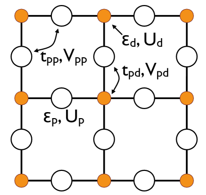
The model has a CuO2 unit cell consisting of a orbital on the Cu site and orbitals on the and oxygens. In a representation in which the vacuum of the 3-orbital model has the configuration (), and create holes with spin on the Cu and O sites respectively, and the Hamiltonian has the form
| (1) | |||||
| (2) | |||||
| (3) | |||||
| (4) |
Here is the energy difference between having a hole on an O site versus a Cu site, and are one-hole hopping matrix elements between near-neighbor Cu and O sites and near-neighbor O sites, respectively. The sums in Eq. 4 denote sums over the relevant nearest-neighbor sites. and are the onsite Cu and O Coulomb interactions and and are the nearest-neighbor Cu–O and O–O Coulomb interactions, respectively. The phases of the orbitals have been fixed such that the signs of the hopping matrix elements remain the same throughout the lattice and are positive.
The hopping parameters and found for La2CuO4 and Nb2CuO4 in various cluster and LDA calculations are relatively close to each other. We will measure energies in units of and set for both of these materials ref:5 ; ref:15 . The primary difference in the one-electron parameters occurs in where the absence of the apical oxygens in Nd2CuO4 is expected to lead to a reduction in relative to La2CuO4. Indeed this is found in LDA calculations, however the appropriate bare values of to use in the 3-orbital Hamiltonian Eq. (4) has posed a problem because of double counting corrections ref:16 ; ref:17 . Here we find that setting gives reasonable values for the charge gap and exchange interaction. Thus, working in units of we will take for a canonical set of parameters
| (5) |
These parameters are appropriate for a charge transfer system for which and . Using a similar set of parameters for a 2-leg CuO2 ladder we previously found at half-filling a charge gap and a spin gap . For a 2-leg ladder the effective exchange coupling . For of order 1 to 2 eV, these correspond to reasonable values for the charge gap and the exchange interaction. Our plan is to use this same set of parameters for both the hole and electron doped systems and focus on the differences that arise between them. We will comment on the effect of reducing and, for the electron doped case, the effect of reducing .
The DMRG calculations will be carried out for an CuO2 lattice which has periodic boundary conditions in the 4-unit cell -direction and open ends in the 8-unit cell -direction. For the charge and spin studies, we will work with a fixed number of holes and a hole density per CuO2 unit cell which is 1 for the undoped system. Positive values of () correspond to hole doping and negative values of () to electron doping. We typically did 15 DMRG sweeps, keeping up to states on the last sweep. This led to excellent convergence for the local quantities that we report here. A typical maximum truncation error was ; extrapolating the truncation error to zero gave typical fractional errors in the total energy also about . Without extrapolation, fractional errors in energy were estimated to be less than , and absolute errors in local quantities were in the range . The good overall convergence for this cluster suggests that wider systems, say up to width , will be accessible for near-future studies.
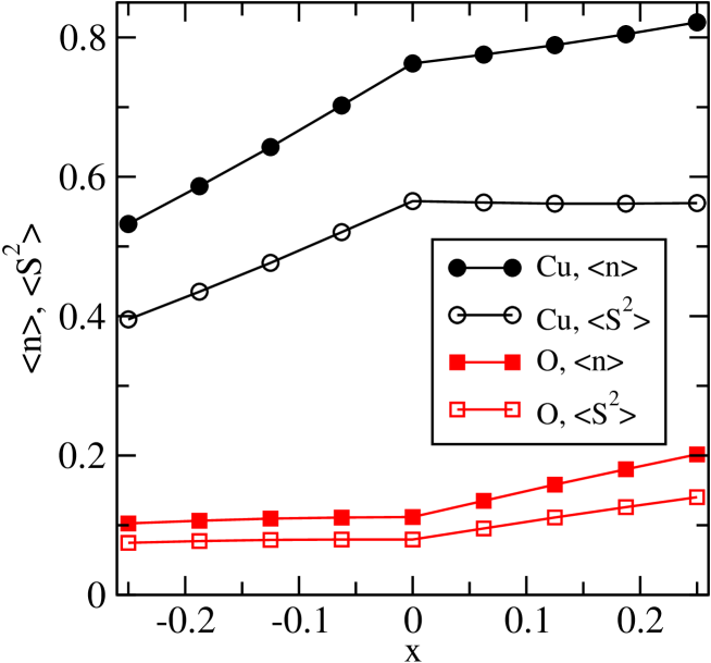
In Fig. 2 we show the effect of doping on the local charge density and squared spin moments on the Cu and O sites as a function of the hole density . As we will discuss later, there can be inter- and intra-cell spatial structure in the charge and spin. The results shown in Fig. 2 represent site averages taken over the lattice. For the undoped () system where there is one hole per CuO2 unit cell, Fig. 2 shows that the hole occupation is approximately 80% on the Cu site and 10% on each of the two O sites for the parameters that we have chosen. When additional holes are added they go approximately 75% onto the two O sites and 25% onto the Cu site of the unit cell. Alternatively, under electron doping, the added electrons go approximately 90% onto the Cu site and only 10% onto the two O sites. This is of course what one would expect for a charge-transfer system. The change in the square of the spin moments on the Cu and O sites is seen to vary with the hole concentration in a similar manner to that of the charge occupation. For electron doping (), an electron added to a Cu site removes the hole spin moment leading to a decrease in averaged over the lattice, while for hole doping the square of the O hole spin moment increases as holes are primarily added to the O sites.
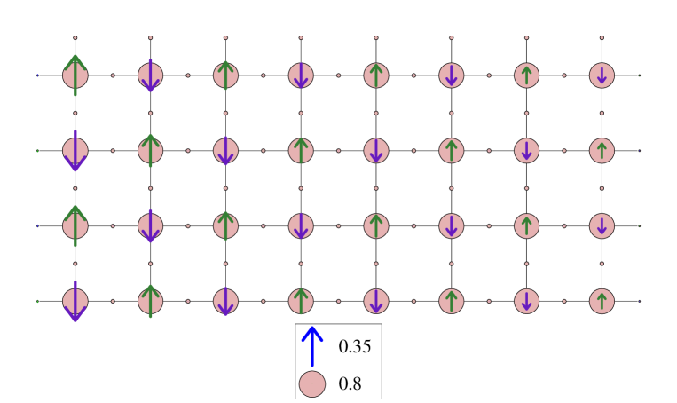
To study the longer range spin and charge correlations, we have applied a weak staggered magnetic field to the Cu sites on the left hand edge of the lattice. The expected antiferromagnetic response of the undoped system is shown in Fig. 3. Here, the diameters of the circles are proportional to the density of the holes and the lengths of the arrows are proportional to the spin moments. One sees, as shown in Fig. 2 that the holes are mainly on the Cu sites. The applied edge field has broken the spin symmetry and there is a well formed antiferromagnetic spin pattern.
In Fig. 4 we contrast the results for hole doping on the left with electron doping on the right. In this figure, the hole density distribution of the undoped lattice shown in Fig. 3 has been subtracted.
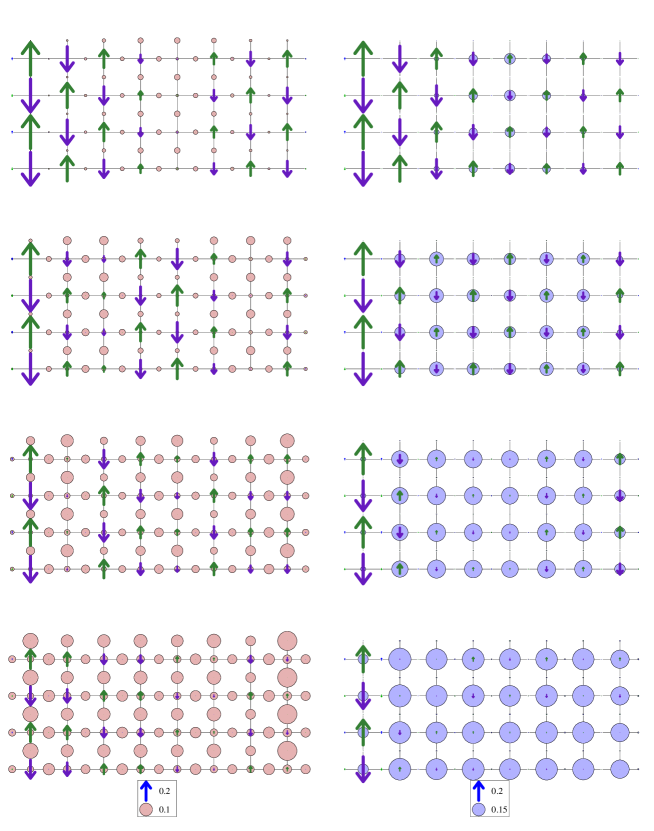
The diameters of the circles for hole doping on the left are proportional to the added hole density while the diameters of the circles on the right are proportional to the added electron density. In this figure the diameter scale used for the hole density is 0.1 and for the electron density 0.15. In the top left hand lattice shown in Fig. 4, 2 holes have been added to the 32 holes of the undoped lattice giving . The lattices shown below this have 4,6 and 8 holes added corresponding to hole concentrations per CuO2 unit cell of 1.125, 1.1875 and 1.25, respectively. The lattices on the right hand side of Fig. 4 show similar results for the case in which electrons are added (or holes removed). From top to bottom these lattices have 30, 28, 26 and 24 holes, respectively, corresponding to , 0.875, 0.8125 and 0.75. As in Fig. 3, a staggered magnetic field () was applied to the Cu sites on the left-hand edge of the lattice.
As shown in Fig. 2, the additional holes tend on average to go onto the O sites, but as seen in Fig. 4 their distribution is not uniform. For hole doping there is a tendency for stripe formation separated by -phase shifts in the antiferromagnetic correlations. For there are two, approximately Cu-site centered, stripes separated by a -phase shifted antiferromagnetic region similar to the well known behavior of La1.48Nd0.4Sr0.12CuO4 ref:6 . For there is a single stripe and for , corresponding to the addition of 6 holes on the lattice, one can see the remnants of a three stripe structure. This structure vanishes for the strongly overdoped case. The stripe spacing for the three lower hole dopings is consistent with the relation and the well known spin and charge incommensurability relation found in the La-based cuprates ref:4 ; ref:6 . A closer look at the structure of the charge and spin distributions for the 1/8 () hole doped lattice is shown in Fig. 5(a). Here a weak staggered magnetic field has been applied to both ends of the lattice. In this case, the hole doped system exhibits bond centered charged stripes separated by -phase shifted antiferromagnetic regions. The charge modulations on the and sites are in phase leading to what was called an –CDW–SDW phase in Ref. ref:10, . There may be an additional small admixture of -CDW. Of course the lattice already breaks C4 symmetry so one expects differences in the and oxygen hole occupations. Increasing leads to an increase in these differences ref:KFG but the symmetry remains dominant.
For the electron doped system, one sees on the right hand side of Fig. 4 that the spin and charge structure appears quite different from the hole doped case. Of course the doped electrons go dominantly on to the Cu sites and initially the small concentration of added electrons are repelled from the open edge boundaries by the “infinite” edge potential. However, for these parameters, by the time the electron doping reaches 0.125, a relatively uniform density of the added electrons is spread over the Cu sites and the antiferromagnetic order remains. A closer look at the 1/8 electron doped lattice is shown in Fig. 5(b). Here one can see that there are two charge stripes but the antiferromagnetic correlations remain commensurate. Thus for these parameters we find charge stripes with incommensurate antiferromagnetism for hole doping and commensurate antiferromagnetic spin correlations for electron doping. This remains the case for the electron doped system when is reduced as is expected in the structure where the apical oxygens are absent. Another important parameter is which determines the effective hopping between next-near neighbor Cu sites. In Hubbard and models it is known that affects the stripe stability ref:8 ; ref:PRB60.R753 . Here we find that when the oxygen-oxygen hopping is reduced, the amplitude of the charge stripes is increased and the spin structure for the electron doped system also becomes incommensurate as shown in Fig. 5(c) for . The effect of reducing acts to increase the frustration associated with the antiferromagnetic background and gives rise to the -phase shifted antiferromagnetic regions separating the charge stripes.
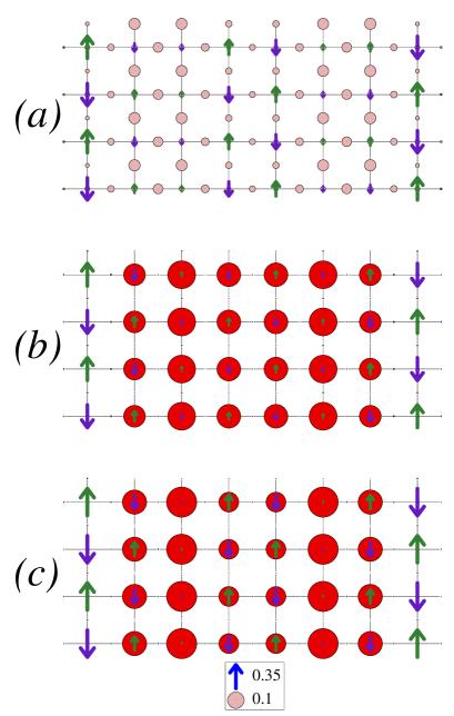
We find that when is reduced (below ), striping can occur for both the electron and hole doped system. However, the tendency for striping is stronger in the hole doped system.
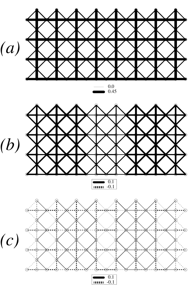
The addition of holes to the filled band vacuum configuration () lowers the kinetic energy. For the hole Hamiltonian, Eq. (4), with positive hopping parameters this means that one expects the Cu-O and O-O hole hopping strengths and to be positive for the 32 hole doped system as illustrated in Fig. 6(a).
The Cu-O hopping strength is larger than the O-O hopping strength reflecting the fact that the doped holes are of order 80% on the Cu sites. When additional holes are added, the hopping strength increases further. The difference in the hopping strengths between the 36 hole doped lattice and the undoped 32 hole lattice are illustrated in Fig. 6(b). In the case of hole doping, the holes are distributed to both the Cu and O sites (% to the Cu and % to each of the O sites) leading to the enhancement of both the Cu-O and O-O hopping strengths shown in Fig. 6(b). In addition, one sees evidence of the charge stripe structure.
For the case of electron doping, the electrons go dominantly on the Cu sites. This reduction of the average number of holes on the Cu sites leads to the reduction in the Cu-O hole hopping strength as shown in Fig. 6(c). Although the reduction of the average hole occupation on each O is only of order 5%, one might have expected that this would also reduce the strength of the O-O hole hopping. However, as shown in Fig. 6(c), the O-O hopping strength is in fact slightly increased. The overall change in hopping strength is significantly smaller for the electron doped system. The total change in the kinetic energy measured in units of per added hole is of order while per added electron it is only . This is consistent with the notion that the doped holes will enter a region of the band between and where there is significant dispersion while the electrons will enter near where the dispersion is flat.
In order to study the pairing response, we have applied a proximity singlet pair-field that couples to near neighbor Cu sites along the direction,
| (6) |
with . The Cu-O near neighbor responses in the -direction has a negative sign and is shown as the dashed lines in Fig. 7.
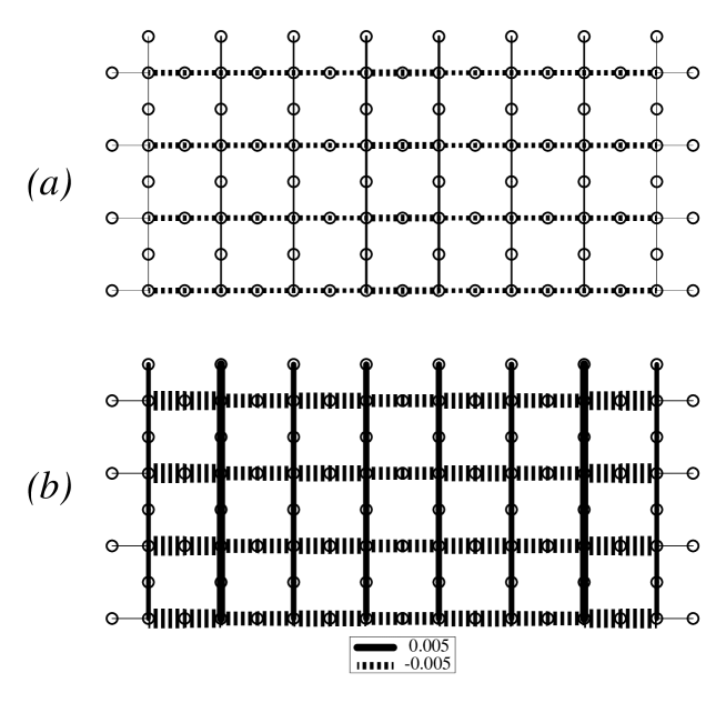
The solid lines, which indicate a positive value, show the pair-field response between near neighbor Cu-O sites in the direction. For these calculations the average hole number was set by a chemical potential . In the top panel, Fig. 7(a), , giving an average hole number () while for the lower panel, Fig. 7(b), giving (). Both the hole doped pair-field response shown in Fig. 7(a) and the electron doped case shown in Fig. 7(b) have the expected d-wave-like sign change.
If the proximity pair-field is applied only between the horizontal Cu-Cu sites on the left edge of the lattice, the induced pair-field decays rapidly in the x-direction for the hole doped system and somewhat more slowly for the electron doped case. The longer range pair-field correlations are suppressed by finite size effects. These are particularly severe for the periodic in (tube-like) geometry of our CuO2 lattice. As seen in Fig. 4 for the hole doped lattice, a stripe appears each time a pair of holes is added for 2, 4 and 6 holes. This is consistent with previous 2-leg ladder studies where it was found that the preferred filling was 2 holes per 4 rungs ref:PRL80.1272 ; ref:PRB60.R753 . Thus for an CuO2 tube a low-energy fluctuation of holes involves the creation or destruction of a stripe, leading to a high energy spin configuration with a domain wall without holes. Alternatively, one could consider a configuration which has 4 holes in a stripe, but this is also energetically unfavorable. While this effect is less severe for the electron doped system shown in Fig. 7(b) and the pair-field response is stronger because it lacks the antiferromagnetic domain walls, we expect that the small size of the lattice still acts to suppress the hole number fluctuations. Properly comparing the pairing between the electron doped and hole doped systems will require larger systems, and if there are stripes they should be long, running lengthwise down the cylinder, either horizontally or spiraling.
In summary, we have studied an three orbital Hubbard model for CuO2 with parameters chosen to give a realistic charge gap and exchange coupling. With one hole per CuO2 unit, the hole occupation is approximately 80% on the Cu orbital and in the presence of a weak staggered edge magnetic field commensurate antiferromagnetic correlations are found to extend across the lattice. When additional holes are added they go % onto the O sites and charge stripes separated by -phase shifted antiferromagnetic regions appear. The O hole occupation and the Cu spin structure has an -CDW-SDW like structure ref:10 . When additional electrons are added, they go approximately 90% onto the Cu orbitals. For our small cluster, there is a weak tendency for charge modulations but the antiferromagnetic spin correlations remain commensurate. However, when the oxygen-oxygen one electron hopping is reduced, a clear striped structure appears with incommensurate antiferromagnetic correlations. For both the hole and electron doped systems, the response of the -near-neighbor Cu-Cu pair-field is out of phase (-wave like) with respect to the -near neighbor Cu-Cu pair-field induced by an applied -near-neighbor proximity pair-field. These pair-field correlations are short range reflecting the finite size and geometric restrictions of the CuO2 cluster studied.
We would like to thank J.C.S. Davis, S.A. Kivelson, M.A. Metlitski, S. Sachdev and J.M. Tranquada for insightful discussions. SRW acknowledges support from the NSF under grant DMR-1161348 and from the Simons Foundation through the Many Electron collaboration. DJS acknowledges the support of the Center for Nanophase Materials Science at ORNL, which is sponsored by the Division of Scientific User Facilities, U.S. DOE.
References
- (1) J. Zaanen, G. A. Sawatzky, and J.W. Allen, Phys. Rev. Lett. 55, 418 (1985).
- (2) V.J. Emery, Phys. Rev. Lett. 58, 2794 (1987).
- (3) C.M. Varma, S. Schmitt-Rink, E. Abrahams, Solid State Comm 62, 681 (1987).
- (4) G. Dopf, A. Muramatsu, and W. Hanke, Phys Rev B 41 9264 (1990).
- (5) R. T. Scalettar, D. J. Scalapino, R. L. Sugar, and S. R. White, Phys Rev B 44 770 (1991).
- (6) P.R.C. Kent, T. Saha-Dasgupta, O. Jepsen, O.K. Andersen, A. Macridin, T.A. Maier, M. Jarrell, and T.C. Schulthess, Phys. Rev. B 78, 035132 (2008).
- (7) E. Arrigoni, M. Aichhorn, M. Daghofer and W. Hanke, New J. Physics 11, 055066 (2009).
- (8) John M. Tranquada, AIP Conf. Proc. 1550, 114–187 (2013).
- (9) N.P. Armitage et al., Rev. Mod. Phys. 82, 2421–2487 (2010).
- (10) M. Fujita et al., Phys Rev B 70 104517 (2004).
- (11) Q. Li, M. Hücker, G.D. Gu, A.M. Tsvelik, and J.M. Tranquada, Phys. Rev. Lett. 99, 067001 (2007).
- (12) A. Himeda, T. Kato, and M. Ogata, Phys. Rev. Lett. 88, 117001 (2002).
- (13) E. Berg, E. Fradkin, E.-A. Kim, S.A. Kivelson, V. Oganesyan, J.M. Tranquada, and S.C. Zhang, Phys. Rev. Lett. 99, 127003 (2007).
- (14) A.J. Achkar, F. He, R. Sutarto, Christopher McMahon, M. Zwiebler, M. Hucker, G.D. Gu, Ruixing Liang, D.A. Bonn, W.N. Hardy, J. Geck, D.G. Hawthorn, arXiv:1409.6787.
- (15) K. Fujita, M.H. Hamidian, S.D. Edkins, Chung Koo Kim, Y. Kohsaka, M. Azuma, M. Takano, H. Takagi, H. Eisaki, S. Uchida, A. Allais, M.J. Lawler, E.-A. Kim, Subir Sachdev, J.C. Séamus Davis, Proceedings of the National Academy of Sciences of the USA 111, E3026-E3032 (2014).
- (16) Eduardo H. da Silva Neto, Riccardo Comin, Feizhou He, Ronny Sutarto, Yeping Jiang, Richard L. Greene, George A. Sawatzky, and Andrea Damascelli. arXiv:1410.2253.
- (17) R. Comin et al. , arXiv 1402.5415.
- (18) S.R. White, Phys. Rev. Lett. 69, 2863 (1992); Phys. Rev. B 48, 10345 (1993).
- (19) D. Poilblanc and T.M. Rice, Phys. Rev. B 39, 9749 (1989).
- (20) J. Zaanen and O. Gunnarsson, Phys. Rev. B 40, 7391 (1989).
- (21) K. Machida, Physica C: Superconductivity 158, 192 (1989).
- (22) H. Schulz, Journal de Physique 50, 17 (1989).
- (23) S.R. White and D.J. Scalapino, Phys. Rev. Lett. 80, 1272 (1998).
- (24) S.R. White and D.J. Scalapino, Phys. Rev. B 60, R753 (1999).
- (25) M.A. Metlitski and S. Sachdev, New J. Phys. 12, 105007 (2010); A. Thomson and S. Sachdev, arXiv 1410.3483.
- (26) Jay Deep Sau and Subir Sachdev, Phys. Rev. B 89, 075129 (2014).
- (27) M. H. Fischer, S.Wu, M. Lawler, A. Paramakanti, and Eun-Ah Kim, New Journal of Physics 16, 093057 (2014).
- (28) Erez Berg, Eduardo Fradkin, Steven A. Kivelson, John Tranquada, New J. Phys 11, 115004 (2009).
- (29) Philippe Corboz, T.M. Rice, Matthias Troyer, Phys. Rev. Lett. 113, 046402 (2014).
- (30) Eduardo Fradkin, Steven A. Kivelson, John M. Tranquada, arXiv:1407.4480.
- (31) S. Bulut, W.A. Atkinson and A.P. Kampf, Phys. Rev. B 88, 155132 (2013).
- (32) W.A. Atkinson, A.P. Kampf and S. Bulut, arXiv 1404.1335.
- (33) T.A. Maier, D.J. Scalapino, arXiv 1405.5238.
- (34) E. Jeckelmann, D.J. Scalapino, and S. R. White Phys. Rev. B 58, 9492 (1998).
- (35) S. Nishimoto, E. Jeckelmann, and D.J. Scalapino Phys. Rev. B 66, 245109 (2002).
- (36) K. Haule, T. Birol and G. Kotliar, arXiv:1310.1158 (2013).
- (37) M.S. Hybertsen, M. Schluter, and N.E. Christensen, Phys. Rev. B 39, 9028 (1989).
- (38) S.A. Kivelson, E. Fradkin and T. Geballe, Phys. Rev. B 69, 144505 (2014).