Visualizing the Pt Doping Effect on Surface and Electronic Structure in Ir1-xPtxTe2 by Scanning Tunneling Microscopy and Spectroscopy
Abstract
We report on the Pt doping effect on surface and electronic structure in Ir1-xPtxTe2 by scanning tunneling microscopy (STM) and spectroscopy (STS). The surface prepared by cleavage at 4.2 K shows a triangular lattice of topmost Te atoms. The compounds that undergo structural transition have supermodulation with a fixed wave vector (where is the lattice constant in the monoclinic phase) despite the different Pt concentrations. The superconducting compounds show patch structures. The surface of the compound that exhibits neither the superconductivity nor the structural transition shows no superstructure. In all doped samples, the dopant is observed as a dark spot in STM images. The tunneling spectra near the dopant show the change in the local density of state at approximately -200 mV. Such microscopic effects of the dopant give us the keys for establishing a microscopic model of this material.
pacs:
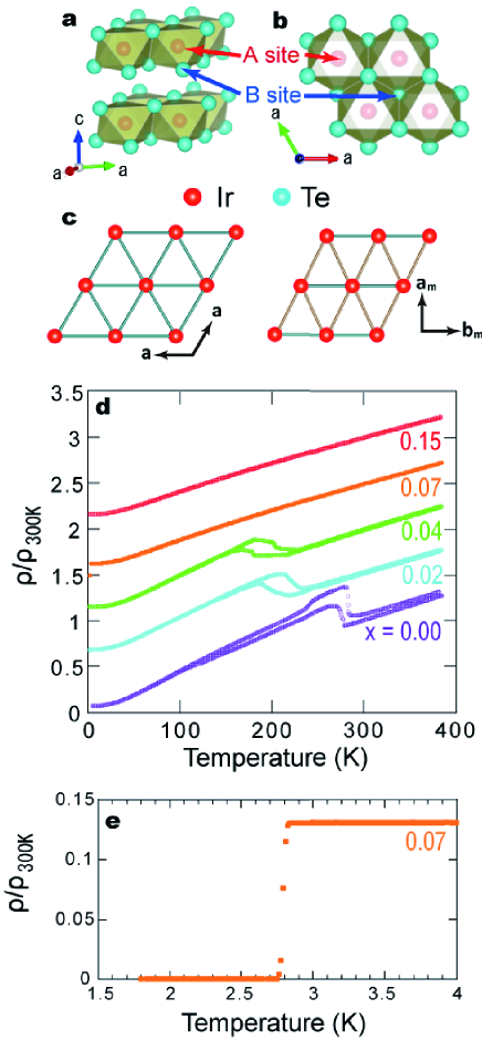
Valid PACS appear hereIn transition metal compounds with electrons, various exotic phenomena are expected because of strong correlation of electrons. One of the most intriguing phenomena is high- superconductivity (SC) in cuprates and iron-based superconductors, which have antiferromagnetic and/or orbital orders in their parent materials. Ir compounds, which also have electrons, have been attracting much attention. Exotic phenomena such as high- SC are expected owing to the competition between the electronic correlation and the spin-orbit interactionWang_1 . Recently, IrTe2 has become a new member of the Ir compound family. This material undergoes a structural transition from trigonal to monoclinic (triclinic) structure at about 280 K accompanied by the abrupt increase in electric resistivity. In the high-temperature phase, the edge-sharing IrTe6 octahedra form a layered structure with an Ir equilateral lattice along the c-axis, as shown in Figs. 1(a) and 1(b). In the low-temperature phase, the Ir lattice changes into an isosceles triangular lattice, and unit cell vectors are also changed to and , as shown in Fig. 1(c). With chemical doping (such as Pt, Pd, and Rh) at the Ir site, the structural transition is suppressed and the SC appears at around 3 KPyon_1 ; Yang_1 ; Kudo_1 . As in the case of iron-based superconductors, it is expected that an ordered state exists below the structural transition temperature () in IrTe2, and the emergence of the SC in doped IrTe2 is related to the disappearance of the ordered state. In IrTe2, the existence of supermodulation (SM) with the wave vector (where is the lattice constant in the monoclinic phase) has been reported from diffractionSeok_1 ; Yang_1 ; Cao_1 ; Pascut_1 ; Toriyama_1 and STMMachida_1 studies. This SM may relate to the expected ordered state. Therefore, it is interesting to investigate how such SM evolves with chemical doping and how the dopant affects the structure and electronic states. To answer these questions, we have performed scanning tunneling microscopy (STM) and spectroscopy (STS) on Ir1-xPtxTe2. We observed SM in the low-temperature phase and patchwork structures in the superconducting sample. Furthermore, Pt sites were identified by STM measurements. The STS measurements revealed the change in the local density of states (LDOS) around -200 mV near the dopant site.
The single crystals used in this study were grown by the self-flux method. In order to determine and the superconducting transition temperature (), we measured the temperature dependence of electric resistivity. The normalized resistivity is shown in Fig. 1(d). The resistivities of the compounds with , and 0.04 show a sudden increase, suggesting the existence of the structural transition. The sample with shows superconducting transition at 2.8 K [Fig. 1(e)]. The compound with shows no superconducting transition above 2 K. The structural and superconducting transition temperatures are summarized in Table I. These results are qualitatively the same as those reported previouslyPyon_2 . However, the reported Pt concentration at which appears is much lower than our nominal value. Furthermore, the same structural transition temperatures () appear at much higher concentrations in our samples than in reported samples. This indicates that, in our single crystals, the actual concentrations of the dopant are expected to be lower than the nominal ones. We used a laboratory-made scanning tunneling microscope for STM and STS measurements. All the measurements were carried out at 4.2 K in He gas. Because of the weak van der Waals coupling between the two Te layers, a clean sample surface is obtained by cleavage at 4.2 K. An electrochemically polished Au wire or a mechanically cut Pt-Ir wire (Pt:Ir = 80%:20%) was used for the STM measurements. A difference in the tips did not affect the results. STM images are obtained in the constant-current mode. The differential tunneling conductance () was obtained by the numerical differentiation of the characteristics.
| Nominal concentration of dopant | Concentration of dark spots | (K) | (K) | Superstructure |
| 0.00 | 0.000 | 280 | - | SM |
| 0.02 | 0.008 | 218 | - | SM |
| 0.04 | 0.01 | 212 | - | SM |
| 0.07 | 0.025 | - | 2.8 | PS |
| 0.15 | 0.073 | - | - | - |
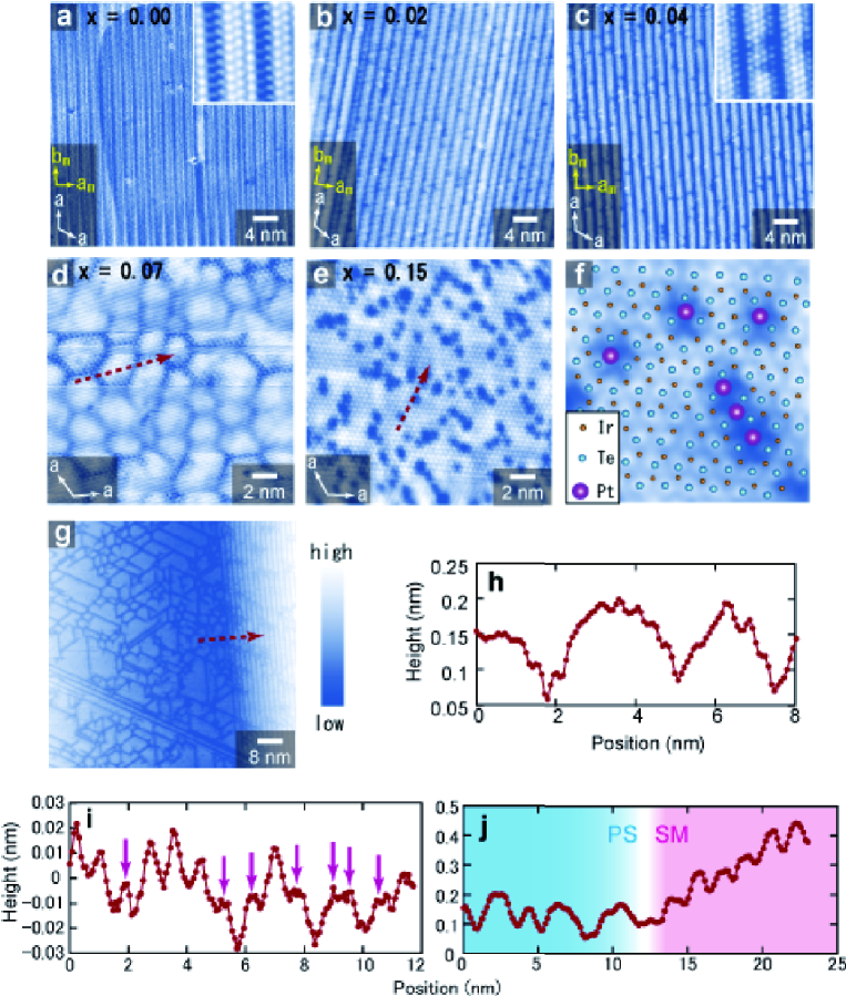
Figures 2(a)-2(e) show typical STM images on Ir1-xPtxTe2 for , and , respectively. The triangular lattice composed of topmost Te atoms can be seen in all images. In addition to the atomic lattice, the SM with , which is the same as that reported previouslyMachida_1 , exists in the compounds with , as shown in Fig. 2(a). The SM with the same modulation wave vector is also observed in the compounds with and 0.04 [Figs. 2(b) and 2(c)]. Thus, the period of the modulation does not change in the low-temperature phase despite the different amounts of the dopant. However, in the compound with , which shows SC, we found that patches with areas of a few nm2 are formed. The surface is randomly paved with patches, as shown in Fig. 2(d). We call this peculiar structure “patchwork structure (PS)”. The boundary of the patches tends to be perpendicular to the Ir-Te bond directions. Note that the SM in the low-temperature phase is also perpendicular to the Ir-Te bonds. The size of the patches is random. Furthermore, in the compound with , which shows neither structural transition nor SC, no superstructure appears, as shown in Fig. 2(e). Thus, the surface structure seems to depend on the ground state of the material. The coexistence of the SM and the PS was seen in a part of the sample, which is perhaps due to the non uniform distribution of the dopant. An example in a sample with is shown in Fig. 2(g). The change in the surface from the SM to the PS is rather abrupt and we have not observed other types of surface structure, such as the SM with a different modulation period. The size of the patch observed in such a region is larger than that observed in Ir0.93Pt0.07Te2 shown in Fig. 2(d).
As can be seen from Figs. 2(b)-2(e), there are several dark spots in STM images on Pt-doped samples. This is easy to see in Fig. 2(e) because of the lack of the SM and the PS. The magnified STM image, shown in Fig. 2(f), reveals that the dark region, which is seen as the dark spots in Fig. 2(e), spreads over the neighboring three Te atoms and the center of the three Te atoms is darkest. This darkest position can be the Ir site (we refer to this site as the A site) or the Te site, which is in the layer below the topmost Te layer (we refer to this site as the B site), as shown in Figs. 1(a) and 1(b). The A and B sites cannot be distinguished by STM measurements, because both sites are located at the center of neighboring the three Te atoms in STM images. However, as can be seen from the STM images in Fig. 2(f), all the darkest positions are connected by a linear combination of the unit vector . This means that all such sites are located in either the A or B site. We found that the number of dark spots changed with Pt doping. We measured the number by counting the dark spots in the STM images. The concentrations of the dark spots are summarized in Table I. Because the concentration of dark spots increases with Pt doping, and all the darkest positions can be A sites, it is plausible that each darkest position corresponds to the Pt site doped at the Ir site. Note that the concentrations of the dark spots are less than the nominal dopant concentrations. This is because, as we mentioned, the actual concentrations in our samples are expected to be less than the nominal ones from the resistivity measurements. Figures 2(h)-2(j) show the cross-sectional profiles of each STM image. These indicate height variations in STM images due to the SM, the boundary of patches, and the dopant. As can be seen from these profiles, the height variation of both the SM and the boundary of patches is about 0.1 nm. On the other hand, the variation due to the dopant is about 0.02 nm.
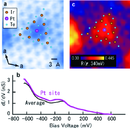
We also observed the dopant effect on the LDOS by STS measurements. As previously reported, the LDOS is modulated by the SMMachida_1 . Thus, such a structure makes the interpretation of the LDOS change by dopants difficult. Therefore, we examined the LDOS change due to the dopant, which is located on a patch in Ir0.93Pt0.07Te2. Figure 3(a) shows an STM image with a dark region, which includes the dopant site. The set bias voltage was 500 mV. The averaged spectrum taken in the dark region (purple) and that in the other region (black) are shown in Fig. 3(b). Both spectra exhibit energy asymmetry, as previously reported Machida_1 . Whereas there is no difference between them above , the enhancement of appears at approximately -200 mV in the dark region, as can be seen in Fig. 3(b). Because is proportional to the LDOS, this enhancement of is related to the change in the LDOS. Figure 3(c) shows a map of the ratio of the tunneling current at -340 mV to that at 340 mV; . This value indicates the ratio of the integrated LDOS between -340 meV and to that between and 340 meV. As can be seen from the figure, the brighter region, which indicates the enhanced LDOS ratio, corresponds to the region where the STM image shows the contrast. The contrast of the STM image comes from both the topographic variation due to the dopant and the LDOS contributions. Thus, the correspondence between the enhancement of LDOS and the STM contrast possibly indicates that the LDOS change is related to the local deformation of the lattice.
We found that the wave vector of the SM does not change in the low-temperature phase despite the increase in Pt concentration. Thus, this wave vector is considered to be inherent in the low-temperature phase. On the other hand, PS changes its average size with Pt concentration, as can be seen from Figs. 2(c) and 2(g). PS may contribute to the reduction of the structural stress due to the Pt dopant. However, the correlation between the appearance of PS and SC is an open question.
As for the electronic states, Ootsuki et al. reported the spectral weight suppression in occupied states in a pristine sample when the temperature is decreased below . They also observed that the spectral weight suppression disappeared with Pt dopingOotsuki_1 . Our observation of the change in LDOS near Pt sites is consistent with this result.
In conclusion, by STM, we have observed a triangular lattice composed of topmost Te atoms and various superimposed structures of Ir1-xPtxTe2 (, and 0.15). The SM with was observed in the compounds with , and 0.04. The PS was observed on the compound with . A modulated surface such as the SM or the PS vanished in the compound with . In all doped compounds, several dark spots due to the Pt dopants are observed. STS measurements revealed that the LDOS at approximately -200 meV is changed by the dopant. These local effects of Pt dopants on IrTe2 will provide considerable information for the establishment of a theoretical model of this system.
References
- (1) F. Wang and T. Senthil, Phys. Rev. Lett. 106, 136402 (2011).
- (2) S. Pyon, K. Kudo, and M. Nohara, J. Phys. Soc. Jpn. 86, 053701 (2012).
- (3) J. J. Yang, Y. J. Choi, Y. S. Oh, A. Hogan, Y. Horibe, K. Kim, B. I. Min, and S-W. Cheong, Phys. Rev. Lett. 108, 116402 (2012).
- (4) K. Kudo, M. Kobayashi, S. Pyon, and M. Nohara, J. Phys. Soc. Jpn. 82, 085001 (2013).
- (5) Y. S. Oh, J. J. Yang, Y. Horibe, and S.-W. Cheong, Phys. Rev. Lett. 110, 127209 (2013).
- (6) H. Cao, B. C. Chakoumakos, X. Chen, J. Yan, M. A. McGuire, H. Yang, R. Custelcean, H. Zhou, D. J. Singh, and D. Mandrus, Phys. Rev. B. 88, 115122 (2013).
- (7) G. L. Pascut, K. Haule, M. J. Gutmann, S. A. Barnett, A. Bombardi, S. Artyukhin, T. Birol, D. Vanderbilt, J.J. Yang, S.-W. Cheong, and V. Kiryukhin, Phys. Rev. Lett. 112, 086402 (2014).
- (8) T. Toriyama, M. Kobori, T. Konishi, Y. Ohta, K. Sugimoto, J. Kim, A. Fujiwara, S. Pyon, K. Kudo and M. Nohara, J. Phys. Soc. Jpn. 83, 033701 (2014).
- (9) T. Machida, Y. Fujisawa, K.Igarashi, A. Kaneko, S. Ooi, T. Mochiku, M. Tachiki, K. Komori, K. Hirata, and H. Sakata, Phys. Rev. B 88, 245125 (2013).
- (10) S. Pyon, K. Kudo, M. Nohara, Physica C 494 (2013) 80.
- (11) D. Ootsuki, Y. Wakisaka, S. Pyon, K. Kudo, M. Nohara, M. Arita, H. Anzai, H. Namatame, M. Taniguchi, N. L. Saini, and T. Mizokawa. Phys. Rev. B 86, 014519 (2012).