Plasmons on the Edge of MoS2 Nanostructures
Abstract
Using ab-initio calculations we predict the existence of one-dimensional (1D), atomically confined plasmons at the edges of a zigzag nanoribbon. The strongest plasmon originates from a metallic edge state localized on the sulfur dimers decorating the Mo-edge of the ribbon. A detailed analysis of the dielectric function reveals that the observed deviations from the ideal 1D plasmon behavior result from single-particle transitions between the metallic edge state and the valence- and conduction bands of the MoS2 sheet. The Mo- and S-edges of the ribbon are clearly distinguishable in calculated spatially resolved electron energy loss spectrum owing to the different plasmonic properties of the two edges. The edge plasmons could potentially be utilized for tuning the photocatalytic activity of MoS2 nanoparticles.
Plasmons are collective electronic excitations that couple strongly to external fields such as light or fast propagating charges. In metals, their excitation gives rise to charge oscillations which can be localized either in the interior of the metal a or at its surface. Localized surface plasmon resonances (LSPR) in metal nanoparticles have been utilized for chemical sensing Kneipp et al. (1997), cancer treatment Au et al. (2008) and to increase solar cell performance Atwater and Polman (2010). Two-dimensional (2D) plasmons are found at metal surfaces and thin films Pitarke et al. (2007), in graphene Chen et al. (2012); Grigorenko et al. (2012); Wunsch et al. (2006); Hwang and Sarma (2007), and other atomically thin 2D materials such as metallic transition metal dichalcogenides Andersen and Thygesen (2013).
Compared to their 2D counterparts one-dimensional plasmons have been much less studied. So far, true atomically confined 1D plasmons have only been observed in self-assembled atomic chains on semi-conducting substrates Nagao et al. (2006); Krieg et al. (2013). One peculiar fundamental aspect of 1D metals is the break down of Fermi-liquid theory and the transition to Luttinger liquid behavior Haldane (1981); Voit (1995): At low energies the spectral weight of the quasiparticle peak approaches zero and the life-time broadening becomes of the same order as the excitation energy Yacoby et al. (1996); Bockrath et al. (1999). This implies that for (ideal) 1D metals, the plasmons adopt a special status as the only excitations which can couple to external fields.
Recently, the interest in novel 2D materials, such as graphene and monolayer , has been accelerated by the prospects of utilizing their unique electronic properties for nanoscale (opto)electronics Mak et al. (2010); Radisavljevic et al. (2011). While graphene has shown great potential as a material for terahertz plasmonics Ju et al. (2011), the finite band gap of MoS2 makes it unsuitable for applications within this field. In a rather different context, MoS2 nanoparticles are used industrially as hydrodesulphurization catalysts Chianelli et al. (2006) and are considered as promising alternative to Pt as low-cost catalysts for hydrogen evolution Jaramillo et al. (2007). The high catalytic activity of the MoS2 nanoparticles has been directly linked to the presence of metallic edges states on the otherwise semi-conducting MoS2 nanoparticles Lauritsen et al. (2003). Very recently, an observed extraordinary photo-catalytic behavior of metallic nanoparticles has been shown to originate from the excitation of LSPRs Christopher et al. (2012); Marimuthu et al. (2013). As we predict here, the the metallic edge states on MoS2 nanostructures can lead to the formation of highly localized 1D plasmons – a result which adds edge-plasmonics to the list of this material’s unique properties with potential applications within nanoplasmonics and photocatalysis.
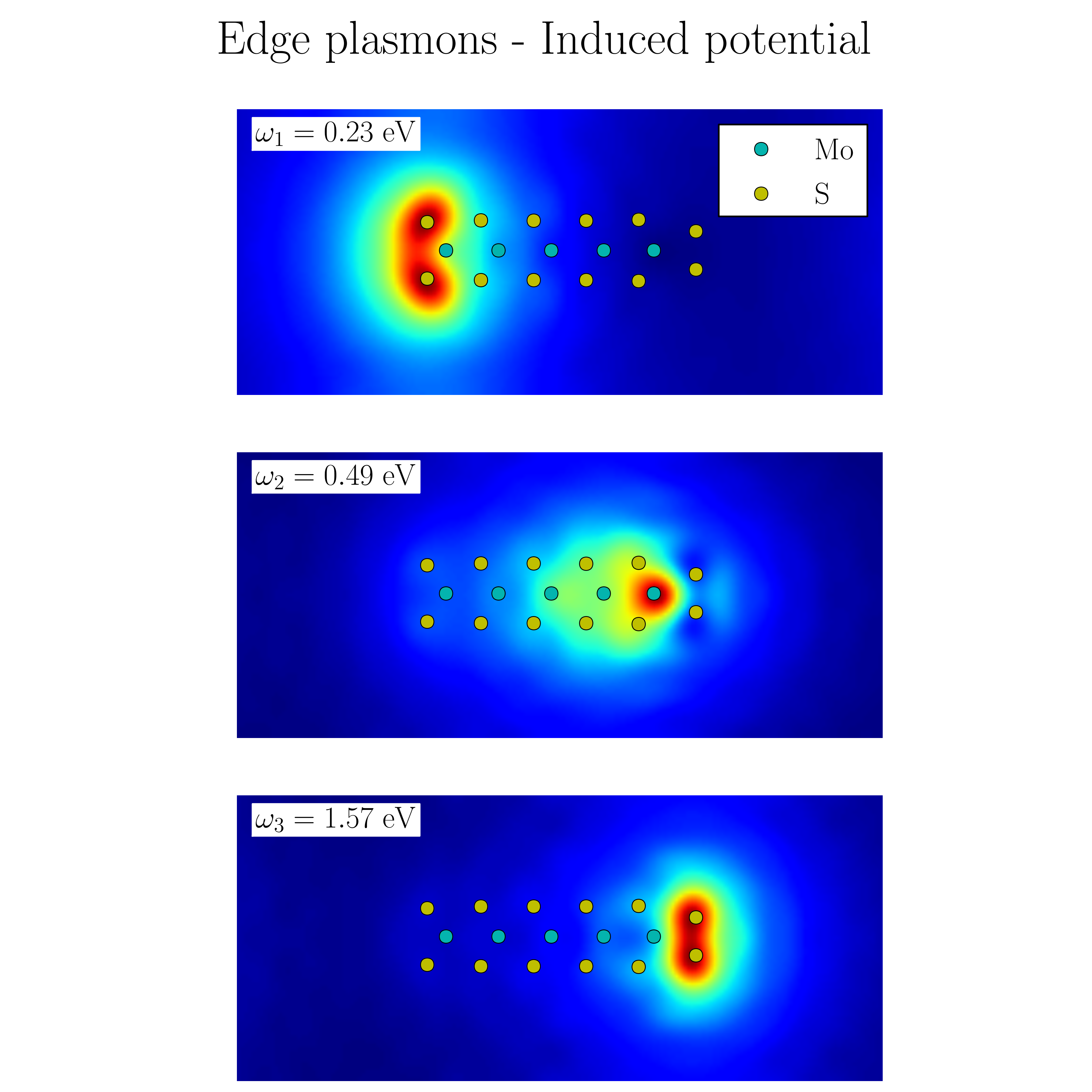
In this communication, we use time-dependent density functional theory (DFT) to demonstrate the existence of a set of highly localized plasmons on the edges of an MoS2 nanoribbon, see Fig. 1. The fundamental properties of this new type of edge plasmon are investigated through a spectral analysis of the dielectric function which allows us to identify the plasmonic eigenmodes of the system in an unambiguous way. The deviations of the edge plasmon properties from those of an ideal 1D plasmon are shown to arise from interband transitions between the metallic edge state and the MoS2 conduction- and valence bands. The distinctly different plasmonic properties of the Mo- and S-edges are clearly seen in the spatially resolved loss spectrum suggesting that high resolution transmission electron microscopy could be used to probe the atomic structure of nanoribbon edges.
All calculations were performed with the GPAW electronic structure code, which is a grid-based implementation of the projector-augmented wave method Enkovaara et al. (2010). We considered a 1.5 nm wide sulfur terminated zigzag MoS2 nanoribbon, see Fig. 1 for a front view of the structure, and supplemental materials for a detailed image of the structure. This edge structure should be favorable at high chemical potential of sulfur, which can be tuned by the choice of sulfiding agent Bollinger et al. (2003). The ribbon was placed in a supercell including 20 and 12 Å of vacuum in the two perpendicular directions. The wave functions were represented in a plane-wave basis set with an energy cutoff of 340 eV. The structure was relaxed using the Perdew-Burke-Ernzerhof (PBE) exchange-correlation functional, while the GLLB-SC functional, including GLLB type exchange by Gritsenko et al. and PBEsol correlation Kuisma et al. (2010), was applied to calculate the single-particle states used as input for the linear response calculation. The GLLB-SC functional has been shown to improve the PBE band gaps of semi-conductors Kuisma et al. (2010) and yield better descriptions of plasmon resonances in noble metals Yan et al. (2011a) due to its improved description of the -band energies. However, for the MoS2 nanoribbon GLLB-SC gives only minor corrections to the PBE band energies. The 1D Brillouin zone was sampled with 128 k-points along the ribbon axis. A spin polarized calculation yielded zero magnetic moment for the structure.
The dielectric matrix was calculated in the random phase approximation (RPA) following reference Yan et al. (2011b):
| (1) |
For the calculation of the non-interacting density response-function, , empty states were included up to 12 eV above the Fermi level, which was sufficient to converge the low energy plasmon peaks of interest. An energy-cutoff of 30 eV was used for the reciprocal lattice vectors and . We used a non-linear frequency grid from 0 to 12 eV, with an initial grid-spacing of 0.01 eV at and a smearing of 0.02 eV. The dense frequency sampling and small broadening was necessary at low energies in order to resolve all intra-band transitions. The Wigner-Seitz truncated Coulomb approximation Sundararaman and Arias (2013) was used in order to avoid interaction between supercells, which would otherwise give a significant energy shift at low momentum transfers.
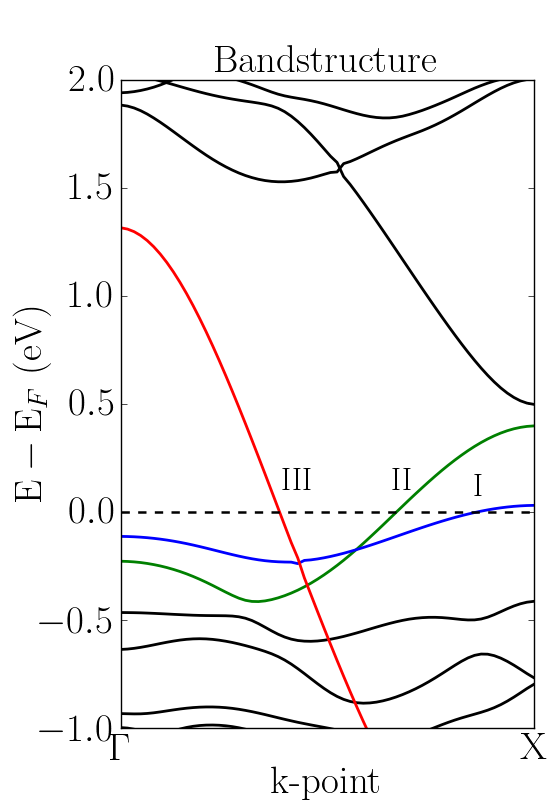
The calculated band structure of the nanoribbon shown in Fig. 2a reveals three metallic edge-states (labeled I-III) in agreement with previous calculations on a nanoribbon with S-terminated edges Bollinger et al. (2003). The remaining bands produce a band-gap of approximately 2 eV. When the width of the ribbon is doubled to 3.3 nm the edge states are unaffected while the bandgap is decreased to 1.8 eV which agrees with the value we find for the infinite single-layer . The Kohn-Sham wavefunctions I and III are almost completely localized on the S-dimers on the S- and Mo- edge of the ribbon respectively. The wavefunctions are linear combinations of -orbitals, forming the one-dimensional metallic states along the edge. (III) has a large Fermi-velocity and is close to linear up to 1 eV away from the Fermi level. The wave function of state II resides at the outermost Mo-atom at the Mo-edge, and extends a few atoms into the ribbon. The number of edge states and their properties depends on the particular edge-configuration. In this case the presence of sulfur dimers on the Mo-edge is crucial for obtaining the state (III). However, zigzag MoS2 nanoribbons are in general found to be metallic opposed to armchair types Pan and Zhang (2012). We note that MoS2 nanostructures could also have topologically protected metallic edge states due to strong spin-orbit coupling in MoS2, which was not included in the present study. In the following we show that the metallic states give rise to plasmon states at the ribbon edges.
The plasmon modes of the system were investigated following a recently developed spectral analysis method for the dielectric function Andersen et al. (2012). The eigenvalue equation
| (2) |
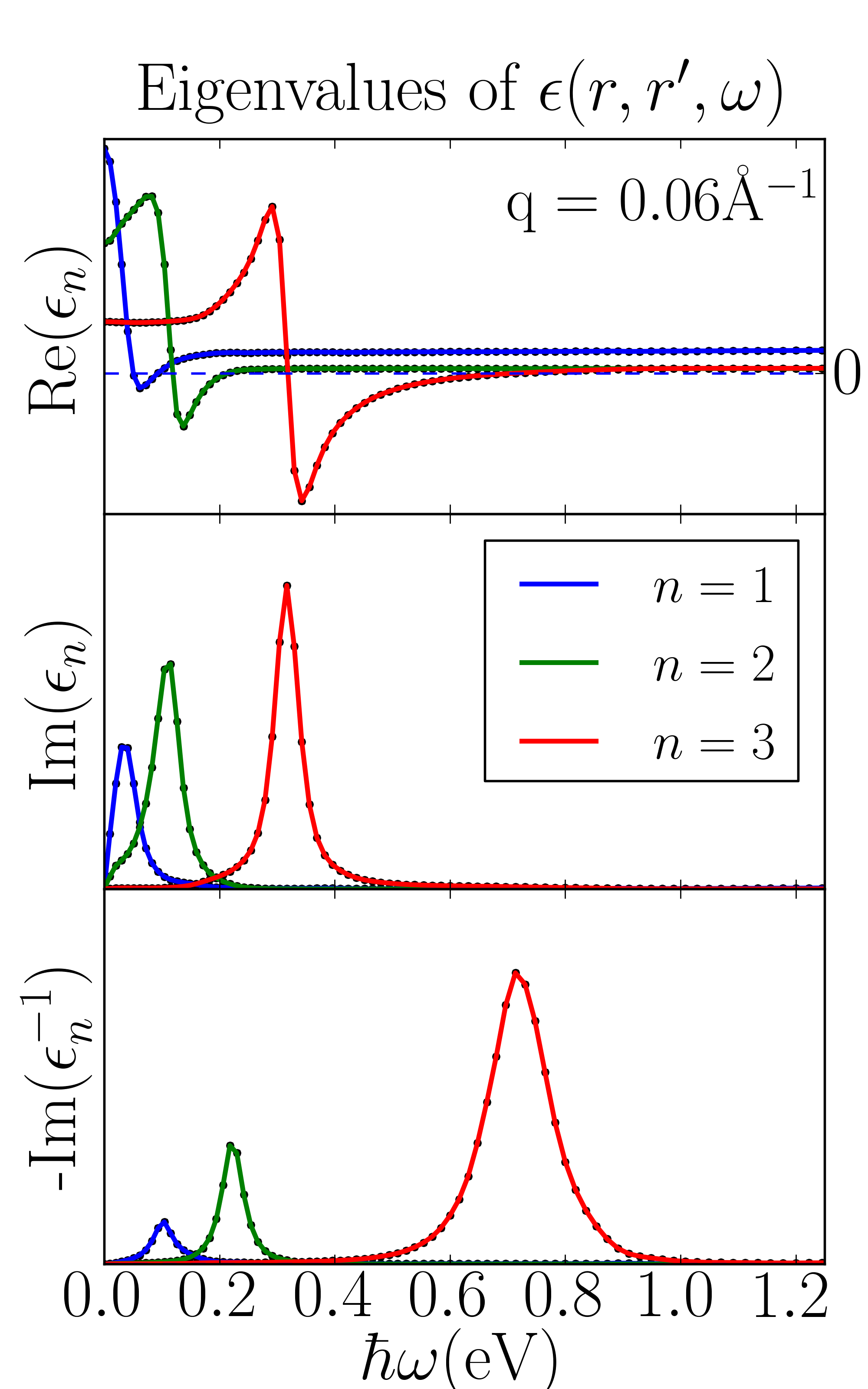
is solved to obtain the frequency-dependent eigenvalues, , and eigenvectors, , of the microscopic dielectric function. The plasmon energies are identified as those frequencies where the real part of an eigenvalue vanishes: . When does not vary too much around the plasmon frequency, a vanishing real part coincide with a maximum in . The corresponding eigenvector gives the spatial form of the induced potential associated with the plasmon oscillation.
For the MoS2 nanoribbon we find three distinct plasmon eigenmodes in the low-energy regime. The dielectric eigenvalue curves corresponding to these modes are shown in Fig. 2b for momentum transfer . Each mode arises from intraband transitions within one of the three metallic edge bands as indicated by the color code. The plasmons are clearly observed as peaks in shown in the lower panel. In contrast, the imaginary parts, , have peaks at the energy of the intra-band transitions associated with the edge-states and occur at . The plasmon has a higher energy than the other two modes, partially due to the larger Fermi velocity of electrons in state (III). The induced potentials of the plasmon eigenmodes, given as the eigenvectors of the dielectic matrix, are shown in Fig. 1. The edge plasmon corresponding to , is clearly localized on the S-dimers of the Mo-edge, and stems from the electronic state (III). The extend of the induced charge density of the edge plasmons are thus limited by the extend of the electronic edge states, so that the plasmons will be atomically localized independently of the size of the MoS2 ribbon.
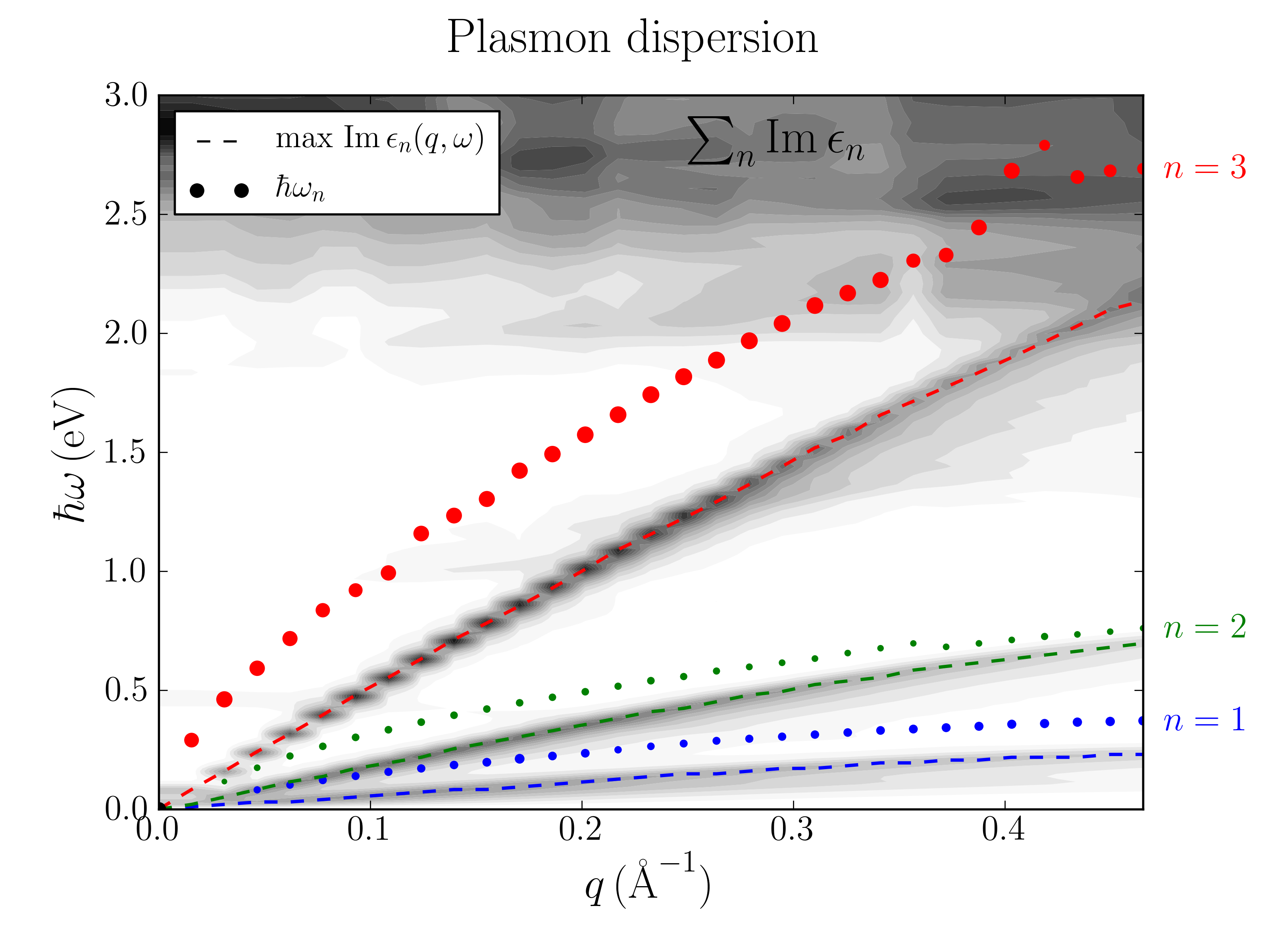
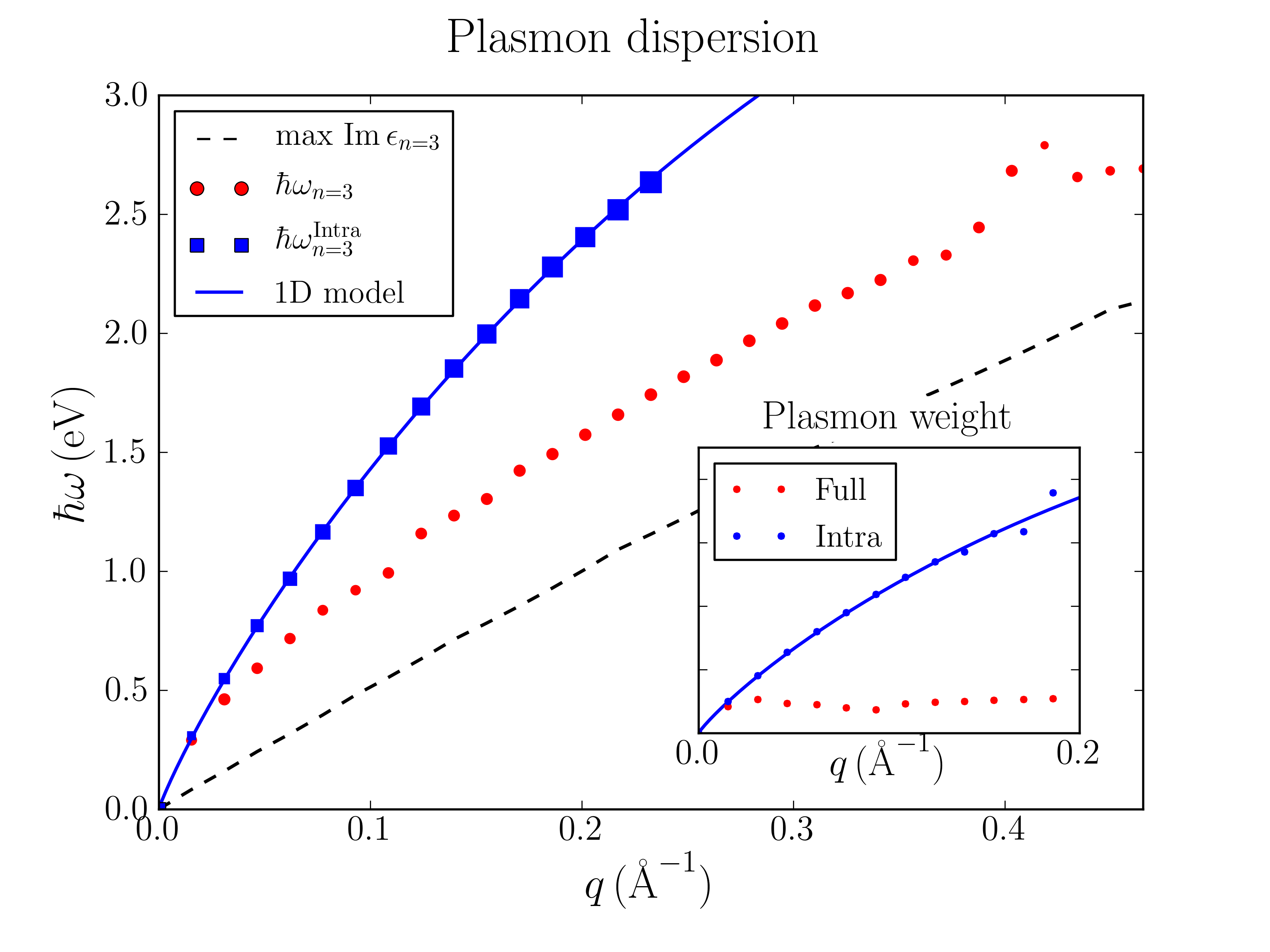
In Fig. 3a the plasmon energies are plotted for increasing momentum transfers, and are clearly seen to be blue-shifted compared the the single-particle intra-band transitions (dashed lines) that disperse linear with . In order to map out the effect of Landau damping in -space, the sum of single-particle transitions, , has been indicated in gray contours. The damping is seen become significant around 2 eV, where inter-band transitions between the valence and conduction band states of the MoS2 sheet set in.
At vanishing momentum transfers, the weight of single-particle transitions decreases significantly, since the number of single-particle transitions scales as . For an ideal 1D electron gas the weight of the plasmon resonance should also go to zero in the limit DasSarma and Hwang (1996). However, our calculations predict that the plasmon weight is almost constant in the considered -range, and actually increases slightly for small momentum transfers. In order to explain this behavior, the result is compared to the pure intra-band plasmon, obtained by including only the single metallic band (III) (see Fig. 2a) in the calculation of . This allows us to compare to the case of an undamped plasmon. As seen in Fig. 3b, this approach yields a plasmon mode that is blue-shifted in energy compared to the full calculation and a weight that approaches zero for small as expected for an ideal 1D metal. Therefore, we conclude that the stagnant weight of the plasmon in the full calculation is due to damping from coupling to interband transitions. The effect of interband transitions can be described by an effective dielectric constant of the medium that screens the Coulomb interaction : . The screened interaction will be reduced in magnitude compared to and will have a finite imaginary part at energies corresponding to the interband transitions. These properties lead to a reduction of energy and life time of the full plasmon compared to the bare intraband result. However, for very low momentum transfers, the plasmon is well separated from single-particle transitions, and a sharp resonance is obtained. Therefore the plasmon coincides with the undamped result, and is expected to have a long lifetime in this regime. For the other two modes, we expect the damping by single-particle transitions to be lesssignificant due to separation in energy.
Following reference DasSarma and Hwang (1996), a simple model for the plasmon dispersion in the long wavelength limit can be obtained by approximating as that of a 1D linear band with transitions at :
| (3) |
The dielectric function is obtained from the RPA expression , where is the 1D Coulomb potential. The inverse dielectric function can then be cast on the form
| (4) |
The pole of for positive frequencies and in the limit of yields the plasmon dispersion
| (5) |
and the weight of the resonance equals . This result is identical to the eigen energies obtained from the interacting Tomonaga-Luttinger model with a 1D Coulomb interaction. In this sense the RPA is exact for a 1D system Li et al. (1992). The Coulomb interaction for a thin wire of confinement can be written for small as , where is a system dependent interaction strength accounting for e.g. the screening due to interband transitions. The expressions for the plasmon frequency and spectral weight derived from the linear band RPA model were fitted to the pure intraband results in Fig. 3b. As expected from the highly linear form of band (III), the quality of the fit is excellent. From the fit we obtained which is in the same order as the radius of the orbitals of the edge state. Comparing the dispersion and weight of the model to the results of the full ab initio calculation, we find agreement for small , after which the plasmon energy and, in particular, the plasmon weight start to deviate in a nonlinear way. This shows that the screening varies as a function of and as is generally the case, such that the interaction strength cannot be written as a constant as assumed in the model.
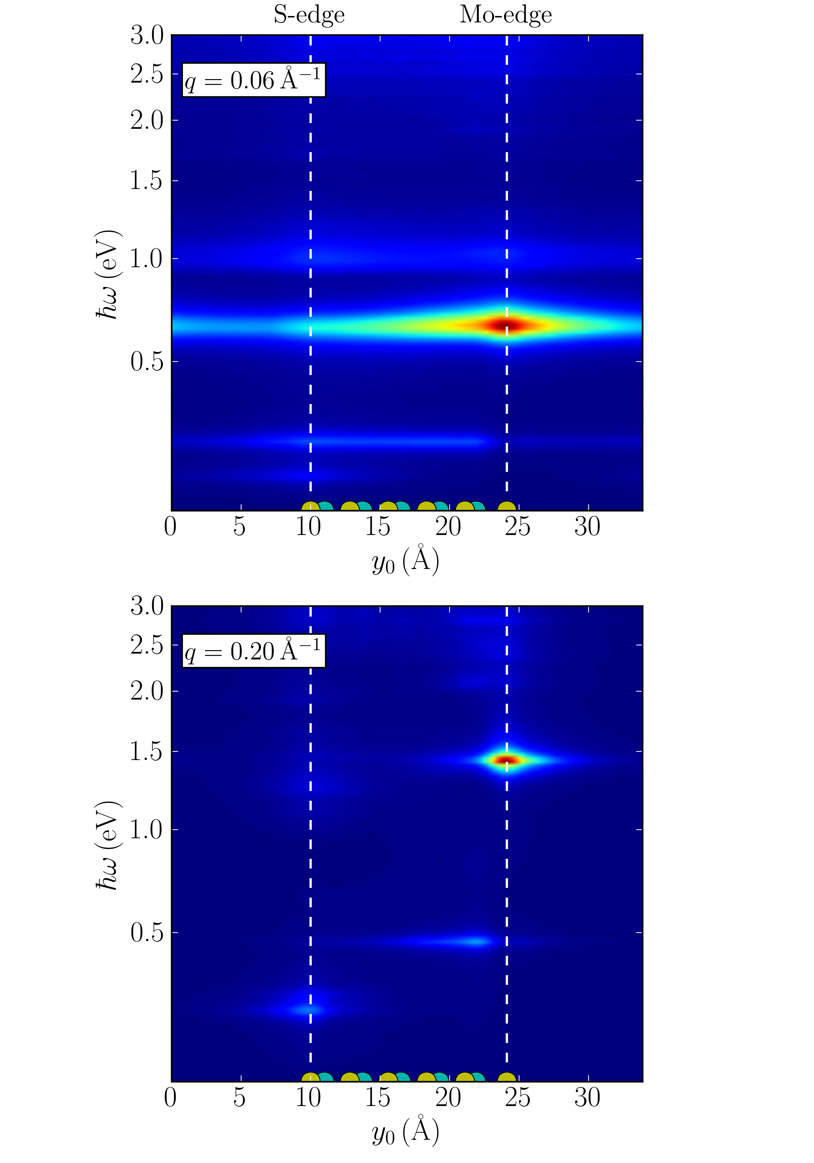
Experimentally, plasmon excitations can be probed by electron energy loss spectroscopy (EELS). When performed with a highly confined electron beam, the spatial form of the loss spectrum can be obtained with few Angstrom resolution García de Abajo (2010).
The loss spectrum is defined as the power dissipated in the medium due to an external potential, :
| (6) |
Here is the imaginary part of the interacting density response function. In the case of EELS, the external potential corresponds to the Coulomb potential of a fast electron moving at constant velocity emitted at point :
| (7) |
The final expression for the loss spectrum is given in the supplemental material sup . In Fig. 4 the spatially resolved EELS spectrum is plotted for two different values of for a beam position that is varied acroos the ribbon. The spectrum is dominated by the S-dimer plasmon on the Mo-edge, which reflects the large coupling strength of this mode. The other two edge plasmons are also visible in the spectrum, particularly at larger momentum transfers where the Coulomb potential is less long ranged, which results in more localized features. Furthermore, the modes can be distinguished by their difference in energy and dispersion with . We suggest this approach could be applied to verify the existence of the edge-plasmons in MoS2 nanoribbons or clusters.
In conclusion, our first-principles calculations predict the existence of a unique type of plasmon localized on the edge of a zigzag nanoribbon. The fundamental properties were investigated in detail and its clear signature in the spatially resolved electron energy loss spectrum was demonstrated. Finally, we proposed that the edge plasmons could be utilized to tune the photocatalytic activity of MoS2 nanoparticles as was recently demonstrated for metal nanoparticles Marimuthu et al. (2013); Christopher et al. (2012).
KST acknowledges support from the Danish Council for Independent Research’s Sapere Aude Program through grant no. 11-1051390. The Center for Nanostructured Graphene (CNG) is sponsored by the Danish National Research Foundation, Project DNRF58.
References
- Kneipp et al. (1997) K. Kneipp, Y. Wang, H. Kneipp, L. T. Perelman, I. Itzkan, R. R. Dasari, and M. S. Feld, Physical review letters 78, 1667 (1997).
- Au et al. (2008) L. Au, D. Zheng, F. Zhou, Z.-Y. Li, X. Li, and Y. Xia, ACS Nano 2, 1645 (2008).
- Atwater and Polman (2010) H. A. Atwater and A. Polman, Nature materials 9, 205 (2010).
- Pitarke et al. (2007) J. M. Pitarke, V. M. Silkin, E. V. Chulkov, and P. M. Echenique, Reports on Progress in Physics 70, 1 (2007).
- Chen et al. (2012) J. Chen, M. Badioli, P. Alonso-González, S. Thongrattanasiri, F. Huth, J. Osmond, M. Spasenović, A. Centeno, A. Pesquera, P. Godignon, A. Zurutuza Elorza, N. Camara, F. J. G. de Abajo, R. Hillenbrand, and F. H. L. Koppens, Nature 487, 77 (2012).
- Grigorenko et al. (2012) A. Grigorenko, M. Polini, and K. Novoselov, Nature photonics 6, 749 (2012).
- Wunsch et al. (2006) B. Wunsch, T. Stauber, F. Sols, and F. Guinea, New Journal of Physics 8, 318 (2006).
- Hwang and Sarma (2007) E. Hwang and S. D. Sarma, Physical Review B 75, 205418 (2007).
- Andersen and Thygesen (2013) K. Andersen and K. S. Thygesen, Physical Review B 88, 155128 (2013).
- Nagao et al. (2006) T. Nagao, S. Yaginuma, T. Inaoka, and T. Sakurai, Physical review letters 97, 116802 (2006).
- Krieg et al. (2013) U. Krieg, C. Brand, C. Tegenkamp, and H. Pfnür, Journal of Physics: Condensed Matter 25, 014013 (2013).
- Haldane (1981) F. Haldane, Journal of Physics C: Solid State Physics 14, 2585 (1981).
- Voit (1995) J. Voit, Reports on Progress in Physics 58, 977 (1995).
- Yacoby et al. (1996) A. Yacoby, H. L. Stormer, N. S. Wingreen, L. N. Pfeiffer, K. W. Baldwin, and K. W. West, Physical review letters 77, 4612 (1996).
- Bockrath et al. (1999) M. Bockrath, D. H. Cobden, J. Lu, A. G. Rinzler, R. E. Smalley, L. Balents, and P. L. McEuen, Nature 397, 598 (1999).
- Mak et al. (2010) K. F. Mak, C. Lee, J. Hone, J. Shan, and T. F. Heinz, Physical Review Letters 105, 136805 (2010).
- Radisavljevic et al. (2011) B. Radisavljevic, A. Radenovic, J. Brivio, V. Giacometti, and A. Kis, Nature nanotechnology 6, 147 (2011).
- Ju et al. (2011) L. Ju, B. Geng, J. Horng, C. Girit, M. Martin, Z. Hao, H. A. Bechtel, X. Liang, A. Zettl, Y. R. Shen, et al., Nature nanotechnology 6, 630 (2011).
- Chianelli et al. (2006) R. R. Chianelli, M. H. Siadati, M. P. De la Rosa, G. Berhault, J. P. Wilcoxon, R. Bearden Jr, and B. L. Abrams, Catalysis Reviews 48, 1 (2006).
- Jaramillo et al. (2007) T. F. Jaramillo, K. P. Jørgensen, J. Bonde, J. H. Nielsen, S. Horch, and I. Chorkendorff, science 317, 100 (2007).
- Lauritsen et al. (2003) J. V. Lauritsen, M. Nyberg, R. T. Vang, M. Bollinger, B. Clausen, H. Topsøe, K. W. Jacobsen, E. Lægsgaard, J. Nørskov, and F. Besenbacher, Nanotechnology 14, 385 (2003).
- Christopher et al. (2012) P. Christopher, H. Xin, A. Marimuthu, and S. Linic, Nature materials 11, 1044 (2012).
- Marimuthu et al. (2013) A. Marimuthu, J. Zhang, and S. Linic, Science 339, 1590 (2013).
- Enkovaara et al. (2010) J. Enkovaara et al., Journal of Physics: Condensed Matter 22, 253202 (2010).
- Bollinger et al. (2003) M. V. Bollinger, K. W. Jacobsen, and J. K. Nørskov, Physical Review B 67, 085410 (2003).
- Kuisma et al. (2010) M. Kuisma, J. Ojanen, J. Enkovaara, and T. T. Rantala, Physical Review B 82, 115106 (2010).
- Yan et al. (2011a) J. Yan, K. W. Jacobsen, and K. S. Thygesen, Physical Review B 84, 235430 (2011a).
- Yan et al. (2011b) J. Yan, J. J. Mortensen, K. W. Jacobsen, and K. S. Thygesen, Physical Review B 83, 245122 (2011b).
- Sundararaman and Arias (2013) R. Sundararaman and T. A. Arias, Physical Review B 87, 165122 (2013).
- Pan and Zhang (2012) H. Pan and Y.-W. Zhang, Journal of Materials Chemistry 22, 7280 (2012).
- Andersen et al. (2012) K. Andersen, K. W. Jacobsen, and K. S. Thygesen, Physical Review B 86, 245129 (2012).
- DasSarma and Hwang (1996) S. DasSarma and E. H. Hwang, Physical Review B 54, 1936 (1996).
- Li et al. (1992) Q. P. Li, S. Das Sarma, and R. Joynt, Phys. Rev. B 45, 13713 (1992).
- García de Abajo (2010) F. J. García de Abajo, Reviews of Modern Physics 82, 209 (2010).
- (35) See Supplemental Material for the derivation of the expression for the the spatially resolved electron energy loss spectrum, shown in Fig. 4. Furthermore we have included a detailed figure of the atomic structure of the MoS2 nanoribbon used for the DFT calculations.