Manuscript submitted to the IEEE/OSA Journal of Lightwave Technology
Full resonant transmission of semi-guided planar waves
through slab waveguide steps at oblique incidence
Manfred Hammer***
University of Paderborn, FG Theoretical Electrical Engineering Warburger Str. 100, 33098 Paderborn, Germany
Phone: ++49(0)5251/60-3560 Fax: ++49(0)5251/60-3524 E-mail: manfred.hammer@uni-paderborn.de
,
Andre Hildebrandt,
Jens Förstner
Theoretical Electrical Engineering, University of Paderborn, Germany
Abstract: Sheets of slab waveguides with sharp corners are investigated. By means of rigorous numerical experiments, we look at oblique incidence of semi-guided plane waves. Radiation losses vanish beyond a certain critical angle of incidence. One can thus realize lossless propagation through 90-degree corner configurations, where the remaining guided waves are still subject to pronounced reflection and polarization conversion. A system of two corners can be viewed as a structure akin to a Fabry-Perot-interferometer. By adjusting the distance between the two partial reflectors, here the 90-degree corners, one identifies step-like configurations that transmit the semi-guided plane waves without radiation losses, and virtually without reflections. Simulations of semi-guided beams with in-plane wide Gaussian profiles show that the effect survives in a true 3-D framework.
Keywords: integrated optics, slab waveguide discontinuities, thin-film transitions, 90-degree waveguide corners, vertical couplers, numerical/analytical modeling.
PACS codes: 42.82.–m 42.82.Bq 42.82.Et 42.82.Gw 42.15.–i
1 Introduction
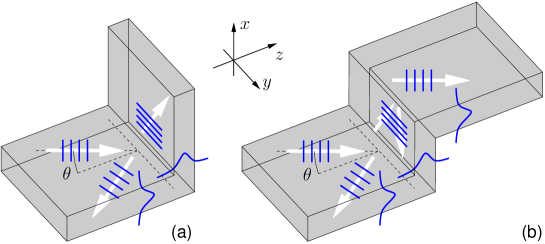
In a conventional 2-D setting, any abrupt discontinuities in a high-contrast dielectric optical slab waveguide typically lead to pronounced radiative losses. This applies also to waveguides with sharp corners. Smooth transitions in the form of waveguide bends [1, 2] help to reduce the losses, but also increase the size of the structures. Perhaps this is why the intriguing propagation characteristics [3] of defect waveguides in photonic crystals, and of 90∘ bends made of these, attracted so much attention, despite their complexity what concerns simulation, design, and experimental realization. With this paper we intend to show that very similar effects can be achieved by much more modest means. To this end, corner and step-like structures as illustrated in Figure 1 are considered, for out-of-plane guided, in-plane unguided plane waves at oblique angles of incidence.
Section 2 introduces a rather general setting of a slab waveguide “discontinuity”, comprising an interior region with in principle arbitrary permittivity, that connects half-infinite slab waveguides at arbitrary positions and angles, but aligned such that the entire structure is homogeneous along one lateral coordinate (the - axis in Figure 1). A general form of Snell’s law applies to pairs of slab modes supported by these access channels. Depending on the modal properties of the incoming and outgoing slabs, one identifies critical angles of incidence that border on regimes with vanishing radiative losses, or on regimes with single-polarization or single mode propagation. Constituting the basis for early concepts of integrated optics [4, 5], this effect has been known for more than four decades (cf. e.g. Refs. [6, 7, 8, 9, 10]), but, to the best of our knowledge, has never been applied to configurations other than simple waveguide facets or transitions between co-aligned slabs with different cross sections, in particular not to configurations with orthogonal access slabs, such as for the present corners or steps.
In Sections 3, 4 we specialize this to high contrast silicon / silicon-oxide slabs. The numerical simulations rely on the vectorial implementation of a scheme for 2-D quadridirectional eigenmode propagation (vQUEP) as described in Ref. [11], based on a former scalar QUEP-variant [12], and building on the bidirectional concepts of Refs. [6, 7]. To investigate in how far the concepts extend to a more practical 3-D setting with at least weak lateral confinement, the propagation of semi-guided, laterally wide Gaussian wave bundles is considered in Section 5. The vQUEP solver [11] has been extended accordingly. A preliminary account of the present findings, highlighting the mechanism for full-transmission across the step, has been given in Ref. [13].
For the present paper our primary interest is in the fundamental effect itself. However, structures as discussed here could e.g. enable power transfer between layers at different vertical levels in an 3-D integrated optical environment, e.g. in a framework of silicon photonics [14, 15]. Beyond the standard evanescent wave interaction [16] between the layers, leading to devices measured in centimeters, for vertical distances below 250 nm [16], or to shorter devices, but for a vertical separation of merely a few tens of nanometers [17], other concepts for vertical coupling include specifically tapered core shapes [18, 19], radiative power transfer through grating couplers [20], or even resonant interaction through vertically stacked microrings [21]. We believe that the concepts from the present paper could offer here a viable, simple and robust alternative, in particular for situations where large lateral extensions of optical channels can be afforded, or if entire layers at different levels need to be uniformly “flooded” by light, e.g. for purposes of optical pumping of active devices.
2 Slab waveguide discontinuities at oblique incidence
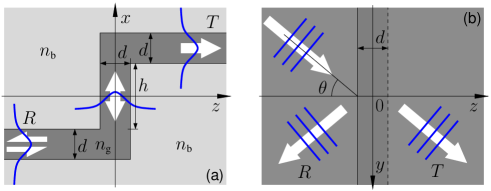
We start with an abstract look at a “discontinuity” in a slab waveguide, as introduced in Figure 2. The structure comprises the slab that supports the incoming and possible reflected waves, possible further slabs that support outgoing waves, and a central region with — what concerns the arguments in these paragraphs — arbitrary properties, hinted at by the dark patch in panel 2(a). In case of the configurations of Figure 1, that region covers the actual corner, or the corners and the vertical segment, respectively. The entire structure is supposed to be constant along the lateral -axis; we choose the -direction as the axis of the incoming waveguide.
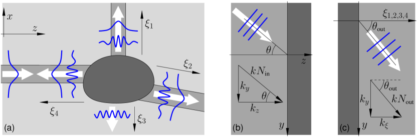
This concerns time harmonic fields with angular frequency , for vacuum wavenumber , vacuum speed of light c , and vacuum wavelength . For the incoming semi-guided wave we assume a polarized guided mode with vectorial profile (see Refs. [7, 11]) and effective mode index , supported by the incoming slab, propagating at an angle in the --plane (cf. Figure 2(b), also Figures 1, 3, 6). The incoming wave thus relates to a field dependence
| (1) |
with , , and . Due to the homogeneity of the problem along , this harmonic -dependence applies to all electromagnetic fields, at all positions; i.e. the global solution can be restricted to a single spatial Fourier component with wavenumber , here given by the angle of incidence .
Next we look at a particular outgoing mode with profile and effective index . As hinted at in Figure 2(a), this can be an actual guided mode supported by one of the slabs with coordinates , , or , but just as well some non-guided, radiated wave propagating in the --plane. The outgoing field (cf. Figure 2(c)) is of the form
| (2) |
where the wave equation [11] requires for the cross-sectional wavenumber , still with fixed by the incoming field.
Depending on the angle of incidence, and specifically for each outgoing mode, one thus has to distinguish between two cases. If the effective mode index is sufficiently large, i.e. if , the outgoing field propagates at an angle with wavenumber , where the effective indices and the angles of incidence and refraction are related by Snell’s law:
| (3) |
Depending on the properties of the supporting slabs, outgoing waves are thus observed each at its own specific angle.
If, on the other hand, the effective mode index is smaller, i.e. if , the outgoing field becomes evanescent with an imaginary wavenumber . For the cross-sectional problem, these waves decay with growing distance . In particular, these evanescent outgoing fields do not carry optical power [22] (but note that they contribute significantly to the total field around the discontinuity).
An increase of the angle of incidence , starting from normal incidence , can thus cause a change of a mode’s type from -propagating to -evanescent. For an outgoing mode with effective index , this happens if . Hence, for given input field and for each individual outgoing mode, by
| (4) |
one can define a characteristic angle , such that this outgoing mode does not carry power for incidence at beyond that critical angle.
With a view to the corners and steps of Figure 1, we now consider a structure where simple symmetric three-layer dielectric slabs, with core and cladding refractive indices and , constitute the (identical) access waveguides (cf. Figures 3, 6). The dimensions are assumed to be such that merely the fundamental modes of both polarizations, with effective indices and , are guided, where . The structure is excited by the fundamental TE mode. In line with the former arguments, one can then conclude:
-
•
All modes of these waveguides that relate to radiative waves, with oscillatory behaviour in the cladding regions (“cladding modes”), have effective indices below the upper limit of the radiation continuum. Their characteristic angles (4) are smaller than the critical angle , defined by , associated with the background refractive index. Consequently all radiation losses vanish for incidence at angles .
-
•
All TM polarized modes supported by these waveguides have effective mode indices below . Their characteristic angles (4) are thus smaller than the critical angle , defined by , associated with the fundamental TM wave. Consequently, for incidence at angles , all incoming optical power is carried away by outgoing fundamental guided TE waves.
Note that these arguments, as well as the former less specific statements, rely solely on the modal properties (1), (2) of the access waveguides, i.e. the reasoning applies to configurations with — in principle — arbitrary interior and arbitrary extension of the region that connects the slab waveguide outlets.
2.1 Formal problem
We complement these more general considerations with a brief look at the rigorous equations, as discussed in Refs. [23, 11]. The problem is governed by the Maxwell curl equations in the frequency domain for the electric field and magnetic field , for uncharged dielectric, nonmagnetic linear media with relative permittivity , for vacuum permittivity and permeability :
| (5) |
The properties of a -homogeneous structure , and of a corresponding harmonic -dependence
| (6) |
of all fields, with the wavenumber given by the incident wave, then lead to a system of vectorial equations on the --cross section plane, here formulated for the two “transverse” electric field components,
| (7) |
with an effective permittivity depending on the angle of incidence:
| (8) |
Eqs. (7), (8) are to be solved on a 2-D domain, with boundary conditions that are transparent for outgoing guided and nonguided waves, and that can accommodate the given influx. Note that the problem coincides formally with the equations for the modes of channel waveguides with 2-D cross sections. The wavenumber appears in place of the channel mode propagation constant. Here, however, the equations need to be solved for the nonstandard boundary conditions, and need to be treated as a nonhomogeneous problem with the influx as a right-hand side, not as an eigenvalue problem as in the case of channel mode analysis.
Details of the quasi-analytical solver (vQUEP, [24]), that has been applied to generate the numerical results of this paper, can be found in Refs. [12, 11]. In all cases the numerical parameters have been selected such that results are converged on the scale of the figures as given, where the power balance (conservation of energy) serves as one of the criteria for convergence. With the exception of the configurations with pronounced radiative losses (small angles of incidence in Figure 4), relatively tight computational windows are sufficient, still with transparent-influx-boundary-conditions that incorporate the incoming waves (other non-guided, radiated fields are suppressed). Similar to guided mode analysis, also here the optical fields are well confined around the guiding cores.
The vanishing of radiative losses for wave incidence beyond the critical angle can be understood just as well in terms of these formal equations [23]. In regions with local constant permittivity , Eqs. (7) reduce to the scalar Helmholtz equation , valid separately for all components of the optical electromagnetic fields, with the angle-dependent effective permittivity (8). Wave incidence beyond the critical angle then leads to a negative local effective permittivity, and consequently to evanescent wave propagation, in the cladding regions with refractive index .
The problem (7) should be distinguished from the standard 2-D Helmholtz problems for TE and TM waves, where the global solutions can be represented by a principal scalar field. The latter emerge from Eqs. (5) if both the structure and the solutions are assumed to be constant along one coordinate axis. In our case that corresponds to normal wave incidence . Still the familiar scalar TE- and TM-slab modes constitute local solutions of Eq. (7), if their vectorial mode profiles are properly rotated [7, 11], and if their cross sectional propagation constants , are modified according to the global wavenumber .
3 Corner discontinuity
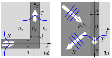
Next we specialize to the corner configurations. Figure 3 introduces a set of parameters that relate to silicon thin film cores in a silicon-oxide background at a typical near infrared wavelength.
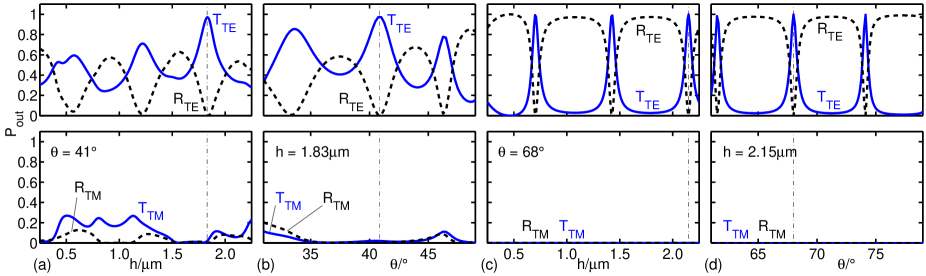
Figures 4, 5, and Table 1 collect the results of a series of rigorous vQUEP simulations for the corner structures. Figure 4 shows the variation of the reflectances , and transmittances , of the fundamental polarized modes with the angle of incidence. As to be expected, only moderate levels of reflection and transmission (cf. Table 1) are observed at normal incidence , with most of the optical power being lost to radiated fields. Pronounced radiative losses are also present at larger angles below , where similar amounts of power are carried upwards by TE- and TM-polarized waves.
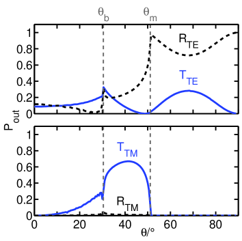
As predicted in Section 2, radiation losses vanish entirely for , beyond the critical angle for propagating waves in the cladding. Power conversion to outgoing TM waves reaches a strong maximum in between and , and is suppressed entirely beyond the critical angle for propagating TM waves, where all outgoing waves are purely TE polarized: for . For even higher angles of incidence one observes a maximum in the TE transmission, which vanishes for grazing incidence as approaches .
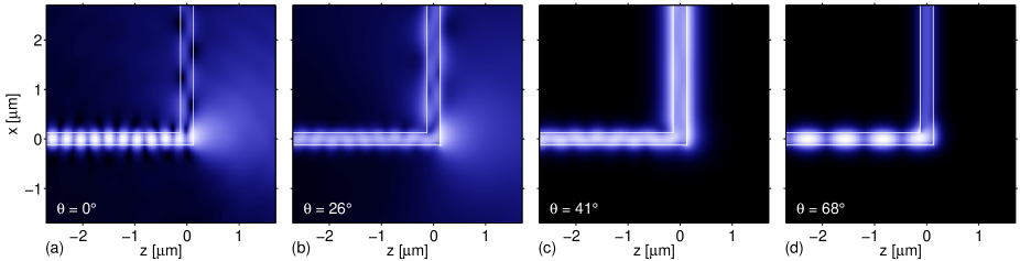
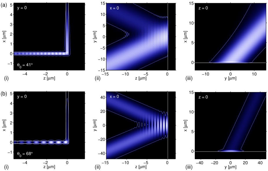
Figure 5 provides a few examples of fields observed for these typical cases. The plots show absolute values of the electric field vector , with the color scales adjusted such that variations in regions with small field strengths become visible. Note that, irrespective of the critical angles, these rigorous solutions contain contributions from the complete sets of local vectorial slab modes, of both polarizations, which are used as the expansions bases [11]. If beyond a related critical angle, however, the then evanescent modes stay localized around the corner region, not contributing to the “far-fields” in the outlets.
While pronounced radiative losses are evident in parts (a) and (b) for , all fields remain confined around the core regions in (c) and (d) for angles . Outgoing TM waves lead to strong electric fields immediately outside the cores of the vertical channel (“highlighted” core edges) in panels (b) and (c), but are absent for the scalar problem at normal incidence (a) and for in (d).
Table 1 compares values for reflectances and transmittances, together with selected parameters, for the configurations of all field plots in this paper. Although here we consider the corners merely as building blocks for the steps of the next sections, a lossless corner structure as the one of Figure 5(c), that channels a total of of the horizontal input into the vertical, might be of practical interest in its own.
| corner | step | u-turn, bridge, stair, s-bend | |||||||||||
| , | |||||||||||||
| n/a | n/a | n/a | n/a | n/a | n/a | ||||||||
| Figure | 5(a) | 5(b) | 5(c) | 9(a) | 5(d) | 9(b) | 8(a) | 10(a) | 10(b) | 8(b) | 10(c) | 10(d) | 11(a, b, c, d) |
4 Step discontinuity
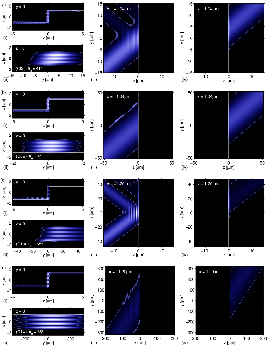
Combination of two of the former corners gives a step structure that connects optical layers at different elevations. Figure 6 introduces coordinates and parameters. Aiming at efficient power transfer, we focus on two of the lossless cases from Section 3, for (Figure 5(c), this will be named configuration C0) and for (Figure 5(d), labeled configuration C1). Both relate to transmission maxima in Figure 4. For each case we assume that the two combined corners are identical.
With the vertical distance between the horizontal layers, only one new parameter appears. Parts (a) and (c) of Figure 7 show the transmittance and reflectance of the step as a function of this distance, calculated by rigorous vQUEP simulations for the full step structure. For both configurations, the angles of incidence exceed the critical angle , hence the steps are lossless.
We look at configuration (C1) first. Since the related corner structures (cf. Figure 5(d), entry in Table 1) transmit and reflect only TE waves, only the upward and downward propagating versions of the fundamental TE mode mediate between the two corners in the vertical part of the step. One might thus compare the step with a standard Fabry-Perot interferometer [25], where the corners play the role of the (identical) partial reflectors. Consequently, the scan over the vertical separation reveals multiple-beam fringes resulting from the interference of the repeatedly up- and downwards reflected TE modes. Maxima with virtually full transmission appear for certain equidistant heights.
Figure 8(b) shows the field pattern for an optimum configuration with full TE-to-TE transmission over a vertical distance of . The field is confined around the core regions, without any beating pattern, i.e. with purely forward waves, in the horizontal segments, and with strong resonant, mostly standing waves in the vertical slab.
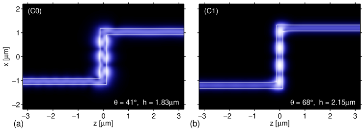
Regarding configuration (C0), at and for TE input, the corners transmit the fundamental modes of both polarizations (with a dominant TM part, cf. the entry of Figure 5(c) in Table 1). Hence, in a step structure made of these corners, one must expect that TM as well as TE waves play a role in the interference in the vertical segment. Accordingly, the scan over the vertical separation in Figure 8(a) shows a much less regular dependence. Still, for a distance , a lossless configuration with virtually full transmission can be identified. The transmission is mostly TE polarized (reciprocity arguments apply [11]), with a TM contribution of about . The field plot in Figure 8(a) shows a major TM contribution to the resonance in the vertical slab, visible through the strong electric field contributions next to the vertical core edges, similar to Figure 5(c).
In principle, given the properties of the constituting corners in the form of scattering matrices, optical transmission through the step structures can be analyzed analytically. For configuration (C1), where propagating TM waves are suppressed, the corners are represented by a matrix that relates to incoming- and outgoing TE waves. Configuration (C0) requires a matrix to accommodate TE as well as TM waves. The model would be applicable to steps of sufficient height, where evanescent fields around the corner regions do not play a role.
As a resonant effect, the property of full transmission must be expected to be sensitive, to some degree, to all parameters that enter. With a view to Section 5 we select the input angle for a further parameter scan. According to panels (b) and (d) of Figure 7, although less perfect in peak performance, configuration (C0) might turn out to be more robust than (C1), here concerning variations of the angle of incidence.
5 Semi-guided beams
All examples discussed in Sections 3 and 4 concern semi-guided plane waves that extend infinitely in the direction. We now look at bundles of the former solutions, for a typically small range of angles of incidence, or of wavenumbers , respectively, with the aim of modeling the incidence of semi-guided, laterally wide but localized beams on the corners and steps. These are wave packets of the form
| (9) |
with a Gaussian weighting of half width , centered around a primary wavenumber , for primary angle of incidence , and an (arbitrary) amplitude . Phase factors have been introduced to position the focus in the --plane at . The central term in curly brackets represents the numerical 2-D vQUEP solution, formally separated into a contribution of the incoming field with mode profile , and a remainder . The integrals are evaluated by numerical quadrature [26]. We thus arrive at approximations of -localized true 3-D solutions, as a basis for the results in Figures 9 and 10.
For a proper choice of wave packet parameters it is instrumental to evaluate the incident part (everything except ) of Eq. (9) a little further. Assuming a small spectral width , and neglecting the effect of the rotation of the vectorial mode profile (by replacing by ), the incident field can be expressed as
| (10) |
with . In the --plane this is a Gaussian beam with fields of full width along at -level, where . By introducing the cross section position and longitudinal position , relative to the focus, as new coordinates through , , one can write the incoming field in the more succinct form
| (11) |
Here the cross-section-width (full width of the field at -level, at focus, in the direction perpendicular to the beam axis) is related to the -width by . Both quantities might be practically relevant, hence both values are listed in Table 1.
Figures 9 and 10 collect corresponding results for our corner and step structures. The plots show the electromagnetic energy density as a physically more relevant quantity. Uniform color scales have been adopted for all three or four panels that relate to different views of the same configuration. In some cases the strong resonant fields visible in the longitudinal views lead to rather dark incoming/outgoing beams (although these carry power of unit order). The single contour at of the energy density maximum is meant to better accentuate the form of these beams.
According to the values in Table 1, both corner configurations work almost identically for bundles with cross section width and for incoming plane waves. The reflected and transmitted beams in Figure 9 remain nicely confined. This can be explained by the mere weak angular dependence of the transmission curves in Figure 4 around the maxima selected for the corner configurations (C0) and (C1).
In contrast, for the same wave bundles of width , the performance of the step structures deteriorates, when compared to the case of plane wave incidence. Here the strong angular dependence of the resonant transmission maxima in Figure 7 becomes relevant. The reflected beams in parts (a, iii) and (c, iii) of Figure 10 show pronounced sidelobes. Merely the central part of the incoming bundle appears to be transmitted. The effect is more pronounced for configuration (C1) than for (C0) due to the narrower transmission peak in Figure 7(d).
Hence we choose wider input beams for both configurations as our last examples. The cross section widths of (C0) and selected for panels 10(b, d) roughly correspond to an angular range around with TE-transmission above , i.e. , and , , respectively, are adjusted such that for all , for . According to Table 1, for incoming beams this wide, the step configurations come reasonably close to their ideal plane-wave performance.
6 Concluding remarks
Semi-guided plane waves at sufficiently high angles of incidence propagate across arbitrary straight slab waveguide discontinuities without any radiation losses. This effect can be understood in terms of a variant of Snell’s law, that relates effective mode indices and angles of incidence and refraction in pairs of access channels. For a quantitative analysis of these configurations, the frequency-domain Maxwell equations reduce to a vectorial 2-D system, to be solved on a computational window with transparent-influx boundary conditions. Our rigorous quasi-analytical solver enables the convenient analysis of structures with general rectangular permittivity distributions. Simulations of high-contrast Si / SiO2 corners lead to the identification of two example configurations with local transmission maxima. A Fabry-Perot-like resonance effect permits to combine two identical corners into step configurations with full transmission of the incoming semi-guided plane wave, i.e. with (numerically) ideal behaviour. Bundles of the former solutions can serve as examples of what happens to semi-guided, laterally localized beams, when incident on the corners or step structures. Our examples show that transmission properties very close to the laterally infinite case can be realized with beams of sufficient width.
Once a working step configuration has been identified, extension to further, perhaps also intriguing examples is obvious. Due to the waveguide symmetry, the transmission properties of the corners is not affected if one changes their direction. This enables u-turn-like structures as in Figure 11(a). Resonant vertical segments in the form of steps or u-turns can be connected by pieces of horizontal slabs of arbitrary length. One is thus led to the bridge-, staircase-, or s-bend-like configurations of Figure 11(b, c, d). Our vQUEP simulations predict transmittance levels in all cases.
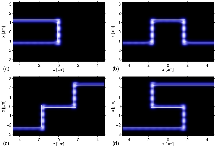
(, ), with an (arbitrary) -distance of between the vertical sections in (b, c, d).
With the exception of the height scan of Section 4, design of the step structures is straightforward, without the necessity of further tuning of parameters. Still there is ample room for optimization: Apart from variations of layer thicknesses, other shapes could be investigated for the refractive index profile of the corner regions. One might aim at a higher transmittance of the single corners, and consequently at a wider angular range of high transmittance for the steps with higher transmission of narrower bundles, preferably for single polarization configurations such as the present (C1). One might also consider structures with true lateral guiding. This would require the preparation of wide channels with weak lateral contrast (e.g. by shallow etching, indiffusion, direct laser writing, or other processes) along the path of the present beams.
Acknowledgments
Financial support from the German Research Foundation (Deutsche Forschungsgemeinschaft DFG, projects HA 7314/1-1, GRK 1464, and TRR 142) is gratefully acknowledged.
References
- [1] E. A. J. Marcatili. Bends in optical dielectric guides. The Bell System Technical Journal, September:2103–2132, 1969.
- [2] K. R. Hiremath, M. Hammer, R. Stoffer, L. Prkna, and J. Čtyroký. Analytical approach to dielectric optical bent slab waveguides. Optical and Quantum Electronics, 37(1-3):37–61, 2005.
- [3] A. Mekis, J. C. Chen, I. Kurland, S. Fan, P. R. Villeneuve, and J. D. Joannopoulos. High transmission through sharp bends in photonic crystal waveguides. Physical Review Letters, 77:3787–3790, 1996.
- [4] R. Ulrich and R. J. Martin. Geometrical optics in thin film light guides. Applied Optics, 10(9):2077–2085, 1971.
- [5] P. K. Tien. Integrated optics and new wave phenomena in optical waveguides. Reviews of Modern Physics, 49(2):361–419, 1977.
- [6] T. P. Shen, R. F. Wallis, A. A. Maradudin, and G. I. Stegeman. Fresnel-like behavior of guided waves. Journal of the Optical Society of America A, 4(11):2120–2132, 1987.
- [7] W. Biehlig and U. Langbein. Three-dimensional step discontinuities in planar waveguides: Angular-spectrum representation of guided wavefields and generalized matrix-operator formalism. Optical and Quantum Electronics, 22(4):319–333, 1990.
- [8] S. Misawa, M. Aoki, S. Fujita, A. Takaura, T. Kihara, K. Yokomori, and H. Funato. Focusing waveguide mirror with a tapered edge. Applied Optics, 33(16):3365–3370, 1994.
- [9] D. N. Chien, K. Tanaka, and M. Tanaka. Guided wave equivalents of Snell’s and Brewster’s laws. Optics Communications, 225(4–6):319–329, 2003.
- [10] F. Çivitci. Integrated Optical Modules for Miniature Raman Spectroscopy Devices. University of Twente, Enschede, The Netherlands, 2014. Ph.D. Thesis.
- [11] M. Hammer. Oblique incidence of semi-guided waves on rectangular slab waveguide discontinuities: A vectorial QUEP solver. Optics Communications, 338:447–456, 2015.
- [12] M. Hammer. Quadridirectional eigenmode expansion scheme for 2-D modeling of wave propagation in integrated optics. Optics Communications, 235(4–6):285–303, 2004.
- [13] M. Hammer, A. Hildebrandt, and J. Förstner. How planar optical waves can be made to climb dielectric steps. Optics Letters, 40(16):3711–3714, 2015.
- [14] R. Soref. The past, present, and future of silicon photonics. IEEE Journal of Selected Topics in Quantum Electronics, 12(6):1678–1687, 2006.
- [15] P. Koonath, T. Indukuri, and B. Jalali. Monolithic 3-D silicon photonics. Journal of Lightwave Technology, 24(4):1796–1804, 2006.
- [16] R. A. Soref, E. Cortesi, F. Namavar, and L. Friedman. Vertically integrated silicon-on-insulator waveguides. IEEE Photonics Technology Letters, 3(1):22–24, 1991.
- [17] J. K. Doylend, A. P. Knights, C. Brooks, and P. E. Jessop. CMOS compatible vertical directional coupler for 3D optical circuits. In Proceedings of SPIE, volume 5970, pages 59700G–10, 2005.
- [18] R. Sun, M. Beals, A. Pomerene, J. Cheng, C.-Y. Hong, L. Kimerling, and J. Michel. Impedance matching vertical optical waveguide couplers for dense high index contrast circuits. Optics Express, 16(16):11682–11690, 2008.
- [19] J. F. Bauters, M. L. Davenport, M. J. R. Heck, J. K. Doylend, A. Chen, A. W. Fang, and J. E. Bowers. Silicon on ultra-low-loss waveguide photonic integration platform. Optics Express, 21(1):544–555, 2013.
- [20] P. Dong and A. G. Kirk. Compact grating coupler between vertically stacked silicon-on-insulator waveguides. In Proceedings of SPIE, volume 5357, pages 135–142, 2004.
- [21] J. T. Bessette and D. Ahn. Vertically stacked microring waveguides for coupling between multiple photonic planes. Optics Express, 21(11):13580–13591, 2013.
- [22] M. Lohmeyer and R. Stoffer. Integrated optical cross strip polarizer concept. Optical and Quantum Electronics, 33(4/5):413–431, 2001.
- [23] F. Çivitci, M. Hammer, and H. J. W. M. Hoekstra. Semi-guided plane wave reflection by thin-film transitions for angled incidence. Optical and Quantum Electronics, 46(3):477–490, 2014.
-
[24]
M. Hammer.
METRIC — Mode expansion tools for 2D rectangular integrated
optical circuits.
http://metric.computational-photonics.eu/. - [25] M. Born and E. Wolf. Principles of Optics, 7th. ed. Cambridge University Press, Cambridge, UK, 1999.
- [26] W. H. Press, S. A. Teukolsky, W. T. Vetterling, and B. P. Flannery. Numerical Recipes in C, 2nd ed. Cambridge University Press, 1992.