Present address: ]Department of Physics, The University of Tokyo, Tokyo 113-0033, Japan
Two-Dimensional Valley Electrons and Excitons in Noncentrosymmetric 3R MoS2
Abstract
We find that the motion of the valley electrons – electronic states close to the K and points of the Brillouin zone – is confined into two dimensions when the layers of MoS2 form the 3R stacking, while in the 2H polytype the bands have dispersion in all the three dimensions. According to our first-principles band structure calculations, the valley states have no interlayer hopping in 3R-MoS2, which is proved to be the consequence of the rotational symmetry of the Bloch functions. By measuring the reflectivity spectra and analyzing an anisotropic hydrogen atom model, we confirm that the valley excitons in 3R-MoS2 have two-dimensional hydrogen-like spectral series, and the spreads of the wave function are smaller than the interlayer distance. In contrast, the valley excitons in 2H-MoS2 are well described by the three-dimensional model and thus not confined in a single layer. Our results indicate that the dimensionality of the valley degree of freedom can be controlled simply by the stacking geometry, which can be utilized in future valleytronics.
pacs:
73.22.-f, 71.20.Nr, 71.35.-y, 78.20.-eI Introduction
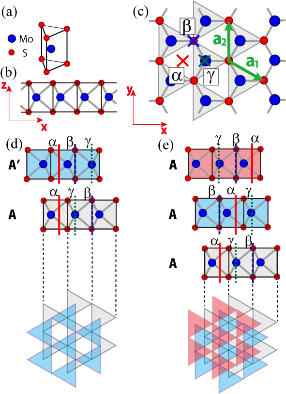
The monolayer systems of group-VI dichalcogenides, (=Mo, W; =S, Se, Te) Novoselov-PNAS2005 have received considerable interest as unique alternatives of graphene for their various intriguing properties Wang-Kis-review2012 : direct band gap of 2 eV Mak-Heinz-PRL2010 ; Splendiani-Wang-NANOlett2010 ; Li-Galli-JPhysChem2007 ; Lebegue-Eriksson-PRB2009 ; Ding-Tang-PhysicaB2011 ; Kuc-Zibouche-Heine-PRB2011 ; Liu-Kumar-IEEE2011 ; Zhu-Schwingenscholgl-PRB2011 ; Ataca-Ciraci-JPhysChem2011 ; Kadantsev-Hawrylak-SSComm2012 , high photoluminescence yield Mak-Heinz-PRL2010 ; Splendiani-Wang-NANOlett2010 , high on/off switching ratio in field effect transistors Kis-MoS2-single ; Yoon-MoS2-single , and electric field-induced superconductivity Taniguchi-super ; Ye-Akashi-super . Most notably, their staggered-honeycomb-like lattice structure (the structure and the unit cell are shown in Fig. 1 (a)–(c)) hosts a model system for valley-dependent phenomena Xiao-PRL2012 originally proposed for graphene Rycerz-valley-filter ; Xiao-graphene-PRL2007 ; Yao-graphene-PRB2008 . The bottom of the conduction band and the top of the valence band are located at the K points of the hexagonal Brillouin zone in . Since the K and K points are not equivalent, the electronic states in the opposite pockets can carry an additional quantum number, the valley index. Furthermore, the spin-orbit coupling results in sizable valley-dependent spin splitting at the valence top (VT). On the basis of the strong coupling between the spin, orbital and valley degrees of freedom, the control of the carrier population of each valley by orbital/spin-sensitive probes has been proposed. Indeed, valley-selective excitation of the electrons and excitons by circularly polarized light has been demonstrated Mak-Heinz-NNano2012 ; Zeng-Cui-Nnano2012 ; Cao-Feng-NComm2012 ; Jones-Xu-WSe2-NNano2013 ; Mak-valley-Hall-Science2014 . Further understanding and stable control of the valley-dependent electronic properties could bring us to the valleytronics—a way of encoding information into the valley degree of freedom, which can be much faster and more efficient than conventional optoelectronics Rycerz-valley-filter ; Xiao-PRL2012 ; Xu-Heinz-review-NPhys2014 .
The above progress led to renewed attention to the rich polymorphism of multilayered Wilson-Yoffe-review ; Wang-Kis-review2012 in view of the valley physics. In inversion-symmetric bilayers with the 2H stacking [Fig. 1 (d)], the net valley-dependent spin polarization is absent. This property has been proposed to be utilizable for switching of the polarization with a symmetry-breaking electric field Wu-efield-NPhys2013 ; Yuan-Saeed-NPhys2013 or mechanical bending Ramasubramaniam-bend . It has also been stated that a layer degree of freedom (upper/lower layer) couples to the valley degrees of freedom Gong-ME-NComm2013 ; Jones-locking-NPhys2014 and this coupling should cause magnetoelectric effects Gong-ME-NComm2013 . On the other hand, very recently, Suzuki et al. Suzuki-MoS2 observed valley-dependent spin polarization in multilayered MoS2 by utilizing the noncentrosymmetric 3R stacking [Fig. 1 (e)]. This success paves a very different way to the control of the valley carriers: Valleytronics by engineering the stacking geometry. However, knowledge of the valley electronic states in the 3R systems is still scarce, which hampers further advances in the field and applications of multilayered MoS2.
In this article, we study the valley electronic states in MoS2 with the 3R stacking and compare them with those in 2H-MoS2. Combining ab initio band structure calculations and group-theoretical analysis, we show that the interlayer hopping amplitude of the valley states is exactly zero in 3R-MoS2, i.e. the electrons are confined within the two-dimensional (2D) layers. Furthermore, we study how this confinement affects the exciton spectrum with an anisotropic hydrogen atom model. Finally, we compare the theoretical results to the reflectivity spectra measured on both 3R-MoS2 and 2H-MoS2 compounds. The revealed mechanism of the single-layer confinement of the valley electrons respects only the crystal and orbital symmetries and therefore is commonly applicable to the family of 3R-, which should facilitate the dimensionality control of the valley states in the transition-metal dichalcogenides.
II Theory on the valley electronic states
II.1 First-principles calculation
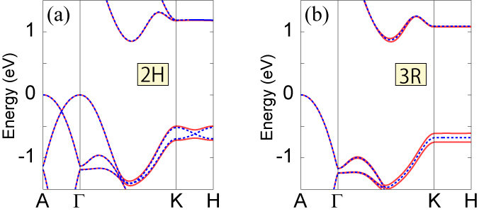
First, we calculated the band structures of bulk 2H- and 3R-MoS2 using the wien2k code employing the full-potential linearized augmented plane-wave method wien2k . We used the Perdew-Burke-Ernzerhof exchange-correlation functional PBE and included the scalar-relativistic effects scalar-rel and spin-orbit coupling SO as implemented in the wien2k code. Experimental lattice parameters and atomic configurations were taken from Refs. MoS2-struct-exp1, and MoS2-struct-exp2, . The muffin-tin radii for Mo and S atoms, and , were set to 2.44 and 2.10 a.u., respectively. The maximum modulus for the reciprocal lattice vectors was chosen so that =7.00.
The calculated band structures are shown in Fig. 2. The apparent difference seen around the point in valence bands is due to Brillouin-zone folding for the 2H case with respect to plane and hence trivial. Notably, along the K–H path, the band at the conduction bottom (CB) is flat for the both polytypes. On the other hand, the VT bands for the 2H polytype shows small but nonzero dispersion, whereas those for 3R is flat. This feature has been first found in Ref. Suzuki-MoS2, but its origin has remained unexplored. Below, we clarify its mechanism analytically.
II.2 Group-theoretical analysis
In order to understand the microscopic origin of the flat bands along the K–H path, let us first look into the symmetries of the electronic states in a monolayer of type in Fig. 1. The little group of K point includes three fold rotation (). Under the rotation around the axis passing through the center of the honeycomb unit [ in Fig. 1(c)], the VT (CB) state, which is formed by Mo 4 (4) orbital having orbital angular momentum (), gets phase 1 () Cao-Feng-NComm2012 .
| A | A’ | |||||||||||
|---|---|---|---|---|---|---|---|---|---|---|---|---|
| VT | CB | VT | CB | |||||||||
| 1 | ||||||||||||
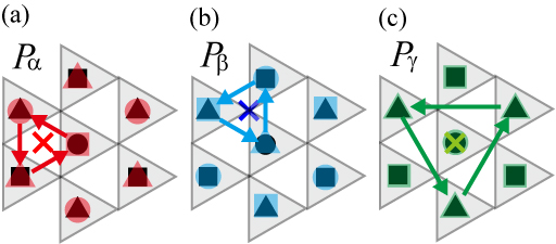
As a matter of fact, there are two more rotational axes inequivalent to : and passing through S and Mo sites, respectively [Fig. 1(c)]. In order to calculate the phase factors for these axes, let us decompose the rotation into two successive operations: permutation of the atomic sites and rotation of the local coordinates at each lattice point . The around axis is defined as (), where denotes the corresponding site permutation. The contribution to the total phase from is simply with =. The contribution from can be calculated by examining how the Bloch wave function transforms under the site permutation. In Fig. 3, the phase of the K-point Bloch state is depicted, where three values (, and ) are represented by circle, triangle and square, respectively. By operating , e.g., the configuration depicted with solid symbols is transformed to that with shaded symbols [panel (a)]. Comparing these symbols on each site, the phase contribution for is deduced. Applying similar arguments to = and , and to the monolayer of type , we get the results summarized in Table 1. Note that the phases for are inverse of those for because their valley states are related by spatial inversion and time reversal.
On the basis of the axis-dependent phases derived above footnote-Yao , let us next consider the interlayer hopping amplitude defined by
| (1) |
for the bulk material. Here, denotes the K-point Bloch functions at th layer, which are eigenstates in the limit where the layer is isolated from others. is the total Hamiltonian of the bulk crystal. Suppose denotes a certain three-fold rotation under which is invariant, then
| (2) | |||||
Here, and denotes the phase summarized in Table 1 for the th layer. Note that and in the second and last lines depend on the stacking pattern and rotational axis of . In the 2H stacking, without loss of generality, we can assume the first and second layers to be and , respectively. In this case, the possible combinations are , and [Fig. 1 (d)], all of which yield and , respectively. In the 3R stacking, where only layers of type are stacked, , , [Fig. 1 (e)], and therefore . According to Eq. (2), the nonzero forces to be zero, which consistently explains the dispersionless bands along the K–H direction in the 3R polytype.
III Valley excitons
III.1 Experiment
The difference in the band structures of 2H- and 3R-MoS2 should cause different optical properties of their valley excitations. To verify this experimentally, we measured the normal incidence reflectivity spectra on the cleaved (001) surfaces of both polytypes at =20 K (see Fig. 4). The details of the crystal growth were reported in Ref. Suzuki-MoS2, . Since the reflectivity were measured in the limited photon energy range of =1.5–3 eV, the spectra were extended up to 30 eV using the data published for 2H-MoS2 MoS2_KK to facilitate proper Kramers-Kronig transformation.
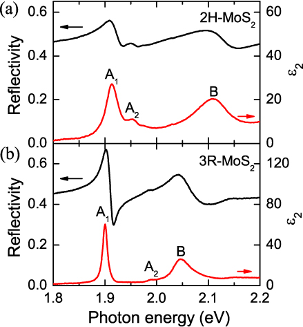
The imaginary part of the dielectric function calculated from the reflectivity is shown in Fig. 4. Although the two main features in the spectra, the and exciton peaks corresponding to the optical excitations from the spin-orbit split VT to the CB, look similar, there are several important differences between the two spectra. First, the energy separation between the and the peaks is larger for the 2H compound (197 meV) compared with the 3R polytype (148 meV), which agrees with the theoretical prediction for the splitting at the VT (see Fig. 2 and Ref. Suzuki-MoS2, ). Beside the main excitonic resonances, smaller peaks were observed on the high energy shoulder of the exciton, labeled as . In a hydrogen-atom-like model of excitons, and are assigned to the 1 and 2 bound states of the electron-hole pair. In the 3R case, and peaks are more separated and their intensity ratio is larger than in the 2H structure.
| 2H | Ours | 16.0 | 10.2 | 0.27 | 1.87 | |
| Ref. epsilon-ref1, | 13.5 | 8.5 | - | - | ||
| Ref. epsilon-ref2, | 16 | 10 | - | - | ||
| Ref. mass-ref1, | - | - | 0.22 (K–), 0.23 (K–M) | 1.7 | ||
| 3R | Ours | 15.9 | 10.1 | 0.24 | 28 |
III.2 Model analysis
To understand these differences, we employed an anisotropic hydrogen atom model anisotropic-hydrogen :
| (3) |
where and are the components of the dielectric constant tensor perpendicular and parallel to the -direction respectively, and and are those of the reduced effective-mass tensor of excitons at the K-point. Note that in a monolayer system, the screened electron-hole interaction is rather different from that in Eq. (3) owing to the surrounding vacuum Keldysh ; nonRydberg . Bulk environment allows us to use the present model as in early studies MoS2-thin-crystals ; exciton-spectr .
The values of , , and were extracted from ab initio calculations using the wien2k code. Dielectric constants were calculated using the random-phase approximation Ehrenreich ; Adler ; Wiser ,
where denotes the volume of the simulation cell, and are indices of the occupied and unoccupied bands, respectively, is the wave vector, denotes the unit vectors, denotes the spin index, denotes the Kohn-Sham wave functions, and denotes their orbital energies. The effective masses were estimated from a parabolic curve fitting of the band dispersions of electrons and holes around the K point within the range of ( for of the 3R polytype). To obtain the effective masses accurately, , , and were set to 2.20 a.u., 1.89 a.u., and 9.00, respectively.
Calculated dielectric constants and reduced effective masses are presented in Table 2, which agree well with previous calculations epsilon-ref1 ; epsilon-ref2 ; mass-ref1 . Since both VT and CB are flat along the K–H line, is quite large in the 3R stacking, whereas it is small in the 2H stacking in which only CB is flat. Note that the effective masses were determined in the close vicinity of the K point, and the valence and conduction bands in 3R-MoS2 have less than 2 meV dispersion along the K–H line. Since this range is much smaller than the binding energy of or exciton, in the following analyses, we regard the 3R bands completely flat, i.e. .
| 2H | Theory | 34 | 8.9 | 25 | 8.2 |
| Expt. | 41.70.8 | 3.70.5 | |||
| 3R | Theory | 81 | 8.9 | 72 | 27 |
| Expt. | 89.60.3 | 395 |
Within the model of Eq. (3), the binding energies and oscillator strengths of the and excitons were estimated. For the 2H case, we referred to a previous report presenting a numerical solution of the model for a range of parameters exciton-spectr . For the 3R case, we instead took the exact solution of the 2D hydrogen atom according to the above consideration. The ratio of the oscillator strengths was derived with the Fermi golden rule Intensity using the present energy eigenvalues and the reduced effective masses. The obtained values are presented in Table 3 together with our experimental ones extracted from fits with Lorentzian peaks (Fig. 4). The substantial differences in the energy levels and in the oscillator strengths between the exciton spectra of the 2H and 3R structures were captured by the model calculation. Since all the parameters in the 2H and 3R cases are similar to each other except , we attribute the differences solely to the 2D confinement of the electrons and holes in the 3R compound.
To see another aspect of the 2H and 3R excitons with respect to their dimensionality, we examined the exciton radii by using a simple trial wave function exciton-variational for the eigenstate of Eq. (3),
| (5) |
with the parameters and , which represent exciton in-plane and out-of-plane radii, respectively, optimized in a variational manner. For the 3R exciton, we used a finite listed in Table 2 to estimate an upper bound of . The obtained values of are almost the same values for the 2H and 3R structures: 19 and 15 Å, respectively. In contrast, the values of are 8.9 and 2.7 Å for the 2H and 3R structures, respectively. Comparing these values with the interlayer distance (6.1 Å for both structures), we can see that the 3R exciton is tightly confined in a single layer while the 2H exciton extends to the neighboring layers.
IV Discussions
The present results establish the 2D nature of the valley exciton in bulk MoS2 with the 3R stacking. Note that an apparently similar confinement effect has also been discussed for the 2H stacking as the spin-layer locking effect Gong-ME-NComm2013 ; Jones-locking-NPhys2014 . Since the magnitude of confinement is governed by the factor with being the spin-orbit coupling coefficient Gong-ME-NComm2013 , its strength essentially relies on atomic number of . Distinctively, the layer-confinement effect in the 3R stacking is a quantum interference effect caused by the symmetry of the crystal and therefore is guaranteed to be relevant in general systems with the same structure. The complete confinement of the 3R valley states should also provide us with an arena of exploring novel interplay of low dimensionality and valley-physics.
Compared to the 2H or monolayer MoS2, the 3R polytype has a significant merit that valley polarized carriers are more robust in the latter form. The carriers are protected from relaxation processes resulting from interlayer transitions, contrary to the 2H systems. In the previous work Suzuki-MoS2 , we have found an indication that interlayer transitions are much suppressed and the valley excitons have much longer lifetime in 3R-MoS2. Now we have clarified that the interlayer hopping amplitude is exactly zero and thus the protection is robust; also, it is common to all 3R-. Note that the 2D states in the 3R systems are different from those in the monolayer systems. In the former, the thickness of the sample allows us to generate valley polarized carriers away from the substrate, which will reduce impacts of the substrate potential. Hence, for example, we can use the 3R crystals as a medium (or lead wires, e.g.) for the valley device, through which the valley-polarized carriers are robustly transmitted. The unique property of the 3R stacking could thus bring about more effective valley-information transmission and generation toward dissipation-less low-energy optoelectronic devices.
V Summary
To summarize, we showed rigorous absence of the interlayer hopping for the valley electrons in 3R-MoS2, which was substantiated with a group theoretical argument. Through the measurement of the reflectivity spectra and analysis with an anisotropic hydrogen atom model, the absence of the hopping has been shown to make the exciton absorption spectrum 2D hydrogen-like and the exciton wave function confined in a single layer. Our results exemplify the control of spatial dimensionality of the valley excitations in 2H- and 3R-, which may help to develop new valleytronics devices.
Acknowledgements.
This work was supported by the Strategic International Collaborative Research Program (SICORP-LEMSUPER), Japan Science and Technology Agency, Funding Program for World-Leading Innovative R & D on Science and Technology (FIRST Program) and Grant-in-Aid for Scientific for Specially Promoted Research (No. 25000003) from JSPS. R. S. was supported by Leading Graduate Program (MERIT) from MEXT. S. B. was supported by Hungarian Research Funds OTKA PD111756 and K108918.Appendix A FITTING OF THE IMAGINARY PART OF THE DIELECTRIC FUNCTION
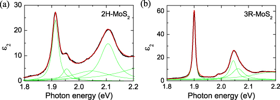
The imaginary part of the dielectric function deduced from the measured reflectivity is fitted by a sum of Lorentzian peaks. The fits shown in Fig. 5 describe the experimental spectra well. The contributions from the higher energy transitions are also included.
References
- (1) K. S. Novoselov, D. Jiang, F. Schedin, T. J. Booth, V. V. Khotkevich, S. V. Morozov, and A. K. Geim, Two-dimensional atomic crystals, Proc. Natl. Acad. Sci. U. S. A. 102, 10451 (2005)
- (2) Q. H. Wang, K. K. Zadeh, A. Kis, J. N. Coleman, and M. S. Strano, Electronics and optoelectronics of two-dimensional transition metal dichalcogenides, Nat. Nanotechnol. 7, 699 (2012).
- (3) K. F. Mak, C. Lee, J. Hone, J. Shan, and T. F. Heinz, Atomically Thin MoS2: A New Direct-Gap Semiconductor, Phys. Rev. Lett. 105, 136805 (2010)
- (4) A. Splendiani, L. Sun, Y. Zhang, T. Li, J. Kim, C. Y. Chim, G. Galli, and F. Wang, Emerging Photoluminescence in Monolayer MoS2, NANO Lett. 10, 1271 (2011).
- (5) T. Li and G. Galli, Electronic Properties of MoS2 Nanoparticles, J. Phys. Chem. C 111, 16192 (2007).
- (6) S. Lebègue and O. Eriksson, Electronic structure of two-dimensional crystals from ab initio theory, Phys. Rev. B 79, 115409 (2009).
- (7) Y. Ding, Y. Wang, J. Ni, L. Shi, S. Shi, W. Tang, First principles study of structural, vibrational and electronic properties of graphene-like MX2 (M=Mo, Nb,W,Ta; X=S, Se,Te) monolayers, Physica B 406, 2254 (2011).
- (8) A. Kuc, N. Zibouche, and T. Heine, Influence of quantum confinement on the electronic structure of the transition metal sulfide S2, Phys. Rev. B 83, 245213 (2011).
- (9) L. Liu, S. B. Kumar, Y. Ouyang, and J. Guo, Performance Limits of Monolayer Transition Metal Dichalcogenide Transistors, IEEE Trans. Electron Devices 58, 3042 (2011).
- (10) Z. Y. Zhu, Y. C. Cheng, and U. Schwingenschlögl, Giant spin-orbit-induced spin splitting in two-dimensional transition-metal dichalcogenide semiconductors, Phys. Rev. B 84, 153402 (2011).
- (11) E. S. Kadantsev and P. Hawrylak, Electronic structure of a single MoS2 monolayer, Solid State Commun. 152, 909 (2012)
- (12) C. Ataca, H. Şahin, and S. Ciraci, Stable, Single-Layer MX2 Transition-Metal Oxides and Dichalcogenides in a Honeycomb-Like Structure, J. Phys. Chem. 116, 8983 (2012).
- (13) B. Radisavlijevic, A. Radenovic, J. Brivio, V. Guacometti, and A. Kis, Single-layer MoS2 transistors, Nat. Nanotechnol. 6, 147 (2011).
- (14) Y. Yoon, K. Ganapathi, and S. Salahuddin, How Good Can Monolayer MoS2 Transistors Be? NANO Lett. 11, 3768 (2011).
- (15) K. Taniguchi, A. Matsumoto, H. Shimotani, and H. Takagi, Electric-field-induced superconductivity at 9.4 K in a layered transition metal disulphide MoS2, Appl. Phys. Lett. 101, 042603 (2012).
- (16) J. T. Ye, Y. J. Zhang, R. Akashi, M. S. Bahramy, R. Arita, Y. Iwasa, Superconducting Dome in a Gate-Tuned Band Insulator, Science 338, 1193 (2012).
- (17) D. Xiao, G. B. Liu, W. Feng, X. Xu, and Wang Yao, Coupled Spin and Valley Physics in Monolayers of MoS2 and Other Group-VI Dichalcogenides, Phys. Rev. Lett. 108, 196802 (2012).
- (18) A. Rycerz, J. Tworzydlo, and W. J. Beenakker, Valley filter and valley valve in graphene, Nat. Phys. 3, 172 (2007).
- (19) D. Xiao, W. Yao, and Q. Niu, Valley-Contrasting Physics in Graphene: Magnetic Moment and Topological Transport, Phys. Rev. Lett. 99, 236809 (2007).
- (20) W. Yao, D. Xiao, and Q. Niu, Valley-dependent optoelectronics from inversion symmetry breaking, Phys. Rev. B 77, 235406 (2008).
- (21) H. Zeng, J. Dai, W. Yao, D. Xiao, and X. Cui, Valley polarization in MoS2 monolayers by optical pumping, Nat. Nanotechnol. 7, 490 (2012).
- (22) K. F. Mak, K. He, J. Shan, and T. F. Heinz, Control of valley polarization in monolayer MoS2 by optical helicity, Nat. Nanotechnol. 7, 494 (2012).
- (23) T. Cao, G. Wang, W. Han, H. Ye, C. Zhu, J. Shi, Q. Niu, P. Tan, E. Wang, B. Liu, and J. Feng, Valley-selective circular dichroism of monolayer molybdenum disulphide, Nat. Commun. 3, 887 (2012).
- (24) A. M. Jones, H. Yu, N. J. Ghimire, S. Wu, G. Aivazian, J. S. Ross, B. Zhao, J. Yan, D. G. Mandrus, D. Xiao, W. Yao, and X. Xu, Optical generation of excitonic valley coherence in monolayer WSe2, Nat. Nanotechnol. 8, 634 (2013).
- (25) K. F. Mak, K. L. McGill, J. Park, and P. L. McEuen, The valley Hall effect in MoS2 transistors, Science 344, 1489 (2014).
- (26) X. Xu, W. Yao, D. Xiao, and T. F. Heinz, Spin and pseudospins in layered transition metal dichalcogenides, Nat. Phys. 10, 343 (2014).
- (27) J. A. Wilson and A. D. Yoffe, The transition metal dichalcogenides discussion and interpretation of the observed optical, electrical and structural properties, Adv. Phys. 18, 193 (1969).
- (28) S. Wu, J. S. Ross, G.-B. Liu, G. Aivazian, A. Jones, Z. Fei, W. Zhu, D. Xiao, W. Yao, D. Cobden, and X. Xu, Electrical tuning of valley magnetic moment through symmetry control in bilayer MoS2, Nat. Phys. 9, 149 (2012).
- (29) H. Yuan, M. S. Bahramy, K. Morimoto, S. Wu, K. Nomura, B.-J. Yang, H. Shimotani, R. Suzuki, M. Toh, C. Kloc, X. Xu, R. Arita, N. Nagaosa, and Y. Iwasa, Zeeman-type spin splitting controlled by an electric field, Nat. Phys. 9, 563 (2013).
- (30) P. Koskinen, I. Fampiou, and A. Ramasubramaniam, Density-Functional Tight-Binding Simulations of Curvature-Controlled Layer Decoupling and Band-Gap Tuning in Bilayer MoS2 Phys. Rev. Lett. 112, 186802 (2014).
- (31) Z. Gong, G.-B. Liu, H. Yu, D. Xiao, X. Cui, X. Xu, and W. Yao, Magnetoelectric effects and valley-controlled spin quantum gates in transition metal dichalcogenide bilayers, Nat. Commun. 4, 2053 (2013).
- (32) A. M. Jones, H. Yu, J. S. Ross, P. Klement, N. J. Ghimire, J. Yan, D. G. Mandrus, W. Yao, and X. Xu, Spin-layer locking effects in optical orientation of exciton spin in bilayer WSe2, Nat. Phys. 10, 130 (2014).
- (33) R. Suzuki, M. Sakano, Y. J. Zhang, R. Akashi, D. Morikawa, A. Harasawa, K. Yaji, K. Kuroda, K. Miyamoto, T. Okuda, K. Ishizaka, R. Arita, and Y. Iwasa, Valley-dependent spin polarization in bulk MoS2 with broken inversion symmetry, Nat. Nanotechnol. 9, 611 (2014).
- (34) P. Blaha, K. Schwarz, G. K. H. Madsen, D. Kvasnicka and J. Luitz, WIEN2k, An Augmented Plane Wave + Local Orbitals Program for Calculating Crystal Properties (Karlheinz Schwarz, Techn. Universität Wien, Austria), 2001. ISBN 3-9501031-1-2 ; http://www.wien2k.at.
- (35) J. P. Perdew, K. Burke, and M. Ernzerhof, Generalized Gradient Approximation Made Simple, Phys. Rev. Lett. 77, 3865 (1996).
- (36) D. D. Koelling and B. N. Harmon, A technique for relativistic spin-polarised calculations, J. Phys. C 10, 3107 (1977).
- (37) J. Kuneš, P. Novak, R. Schmid, P. Blaha, and K. Schwarz, Electronic structure of fcc Th: Spin-orbit calculation with 6 local orbital extension, Phys. Rev. B 64, 153102 (2001).
- (38) K. D. Bronsema, J. L. de Boer, and F. Jellinek, On the structure of molybdenum diselenide and disulfide, Z. anorg. allg. Chem. 540, 15 (1986).
- (39) A. A. Golubichanaya, A. G. Duksina, and V. L. Kalikhman, Variation of the antifriction and electrical properties of a number of solid lubricants with the oxidation temperature, Inorg. Mater., 15, 1156 (1979).
- (40) Note that there are also recent publications Liu-Yao-qdot ; Liu-review utilizing the difference of the phase with and (according to a different notation). The former have addressed coupling between the K and points in the monolayer quantum dot. The latter have discussed the interlayer hopping for the 2H stacking, giving the result consistent with ours.
- (41) G.-B. Liu, H. Pang, Y. Yao, and W. Yao, Intervalley coupling by quantum dot confinement potentials in monolayer transition metal dichalcogenides, New J. Phys. 16, 105011 (2014).
- (42) G.-B. Liu, D. Xiao, Y. Yao, X. Xu, and W. Yao, Electronic structures and theoretical modelling of two-dimensional group-VIB transition metal dichalcogenides, Chem. Soc. Rev. 44, 2643 (2015).
- (43) A. R. Beal, and H. P. Hughes, Kramers-Kronig analysis of the reflectivity spectra of 2H-MoS2, 2H-MoSe2 and 2H-MoTe2 J. Phys. C.: Solid State Phys., 12, 881 (1979).
- (44) G. Dresselhaus, Effective mass approximation for excitons, J. Phys. Chem. Solids 1, 14 (1956).
- (45) L. V. Keldysh, Coulomb interaction in thin semiconductor and semimetal films, JETP Lett. 29, 658 (1979).
- (46) A. Chernikov, T. C. Berkelbach, H. M. Hill, A. Rigosi, Y. Li, O. B. Aslan, D. R. Reichman, M. S. Hybertsen, and T. F. Heinz, Exciton Binding Energy and Nonhydrogenic Rydberg Series in Monolayer WS2, Phys. Rev. Lett. 113, 076802 (2014).
- (47) B. L. Evans and P. A. Young, Exciton Spectra in Thin Crystals, Proc. R. Soc. Lond. A 298, 74 (1967).
- (48) A. Baldereschi and M. G. Diaz, Anisotropy of excitons in semiconductors, Nuovo Cimento 68B, 217 (1970).
- (49) H. Ehrenreich and M. H. Cohen, Self-Consistent Field Approach to the Many-Electron Problem, Phys. Rev. 115, 786 (1959).
- (50) S. L. Adler, Quantum Theory of the Dielectric Constant in Real Solids, Phys. Rev. 126, 413 (1962).
- (51) N. Wiser, Dielectric Constant with Local Field Effects Included, Phys. Rev. 129, 62 (1963).
- (52) T. Cheiwchanchamnangij and W. R. L. Lambrecht, Quasiparticle band structure calculation of monolayer, bilayer, and bulk MoS2, Phys. Rev. B 85, 205302 (2012).
- (53) A. H. Reshak and S. Auluck, Calculated optical properties of 2H-MoS2 intercalated with lithium Phys. Rev. B 68, 125101 (2003).
- (54) H. Peelaers and C. G. Van de Walle, Effects of strain on band structure and effective masses in MoS2, Phys. Rev. B 86, 241401(R) (2012).
- (55) R. J. Elliott, Intensity of Optical Absorption by Excitons, Phys. Rev. 108, 1384 (1957).
- (56) W. Kohn and J. M. Luttinger, Theory of Donor States in Silicon, Phys. Rev. 98, 915 (1955).