Double island Coulomb blockade in (Ga,Mn)As-nanoconstrictions
Abstract
We report on a systematic study of the Coulomb blockade effects in nanofabricated narrow constrictions in thin (Ga,Mn)As films. Different low-temperature transport regimes have been observed for decreasing constriction sizes: the ohmic, the single electron tunnelling (SET) and a completely insulating regime. In the SET, complex stability diagrams with nested Coulomb diamonds and anomalous conductance suppression in the vicinity of charge degeneracy points have been observed. We rationalize these observations in the SET with a double ferromagnetic island model coupled to ferromagnetic leads. Its transport characteristics are analyzed in terms of a modified orthodox theory of Coulomb blockade which takes into account the energy dependence of the density of states in the metallic islands.
pacs:
72.25.-b, 73.23.Hk, 73.63.Kv,I Introduction
(Ga,Mn)As, discovered by Ohno et al. Ohno et al. (1996) nearly two decades ago, is by now the best studied ferromagnetic semiconductor Dietl and Ohno (2014); Jungwirth et al. (2006); Sato et al. (2010). An interesting aspect of this material are large magnetoresistance effects which were discovered in nanofabricated narrow constrictions in thin (Ga,Mn)As films Rüster et al. (2003); Giddings et al. (2005); Schlapps et al. (2006); Ciorga et al. (2007); Pappert et al. (2007); Wunderlich et al. (2006). While the effects were initially interpreted in terms of the tunneling magnetoresistance (TMR) Rüster et al. (2003) and tunneling anisotropic magnetoresistance (TAMR) Giddings et al. (2005), it was proven later that the interplay with Coulomb blockade is also relevant in narrow (Ga,Mn)As constrictions Wunderlich et al. (2006); Schlapps et al. (2009). The origin of this Coulomb blockade anisotropic magnetoresistance (CBAMR) effect are substantial nanoscale fluctuations in the hole density Dietl and Ohno (2014) forming puddles of high hole density separated by low conducting regions. (Ga,Mn)As is known to be a strongly disordered material. Its hole density is close to the metal-insulator-transition. Little variations in the hole density caused by local potential fluctuations can lead to an intrinsic structure consisting of metallic islands separated by insulating areas. It was shown that the magnetoresistance depends, in the presence of Coulomb blockade, not only on an applied gate voltage but can also be tuned by changing the direction of the applied magnetic field Wunderlich et al. (2006); Schlapps et al. (2009). The latter results from the dependence of the Fermi energy on changes in the magnetization and was modeled phenomenologically by Wunderlich et al. Wunderlich et al. (2006). If transport occurs through a narrow nanoconstriction, single electron tunneling (SET) between islands of high carrier density becomes relevant. Thus it is not surprising that the bias and temperature dependence of the magnetoresistance for different magnetization directions could be fitted with a model for granular metals in which metallic islands are separated by insulating regions Schlapps et al. (2009). Because of the nanoscale size of the involved ”metallic” islands, the Coulomb-charging energy is the dominating energy for transport across the nanoconstriction at low temperatures and small bias voltages . Since usually more than one island is involved in transport, Coulomb blockade diamonds, where the resistance is plotted as a function of both bias and gate voltage, revealed a very complex and irregular pattern. Up to now a detailed experimental and theoretical analysis of the Coulomb blockade effects in (Ga,Mn)As nanoconstrictions in the single-electron-transistor regime is still missing.
The aim of this work is a systematic study of the Coulomb blockade effects in nanofabricated narrow constrictions in thin (Ga,Mn)As films. By means of a two step electron beam lithography (EBL) technique we fabricated well defined nanoconstrictions (NC) of different sizes. Depending on channel width and length, for a specific material, different low-temperature transport regimes could be observed, namely the ohmic regime, the single electron tunnelling regime and a completely insulating regime. In the SET regime, complex stability diagrams with nested Coulomb diamonds and anomalous conductance suppression in the vicinity of charge degeneracy points have been observed. In order to understand these observations we propose, for a specific nanoconstriction, a model consisting of two ferromagnetic islands coupled to ferromagnetic leads. We study its transport characteristics within a modified orthodox theory of Coulomb blockade which takes into account the energy dependence of the density of states in the metallic islands.
The paper is structured as follows: Sect. II explains the fabrication process of the samples. In Sect. III the measurement setup is presented. The next section, Sect. IV summarizes the results of the measurements, giving a first interpretation in terms of a double island structure within a classical orthodox model of Coulomb blockade Averin and Likharev (1986, 1991); Grabert (1991); Grabert and Devoret (1992); Sohn et al. (1997); Barnaś and Weymann (2008). In Sect. V, we present the details of the ferromagnetic double island model, study its transport characteristics and make a direct comparison with the experimental results in Sect. VI.1. Conclusions are drawn in Sect. VII.
II Sample fabrication
Our NC-devices were fabricated in a top-down approach starting from a (Ga,Mn)As-layer with a Mn-content of approximately 5. The (Ga,Mn)As layer we used had a thickness of and was grown by low-temperature molecular beam epitaxy on top of a (001)-GaAs substrate. In contrast to the experiments of Schlapps et al. Schlapps et al. (2009) we used as-grown (Ga,Mn)As samples without additional annealing before the sample preparation. First of all, we defined contact-pads for the source- and drain-contacts as well as alignment-marks for the nanopatterning. This was done using optical lithography followed by thermal evaporation of 10 nm Ti and 90 nm Au in a standard lift-off technique. After that, the NC was defined by means of EBL and subsequent chemically assisted ion-beam etching using Cl2. A two-step EBL-process, which allows a precise control of the geometry of the nanocontact and a reliable processing, was developed and is described in Appendix A
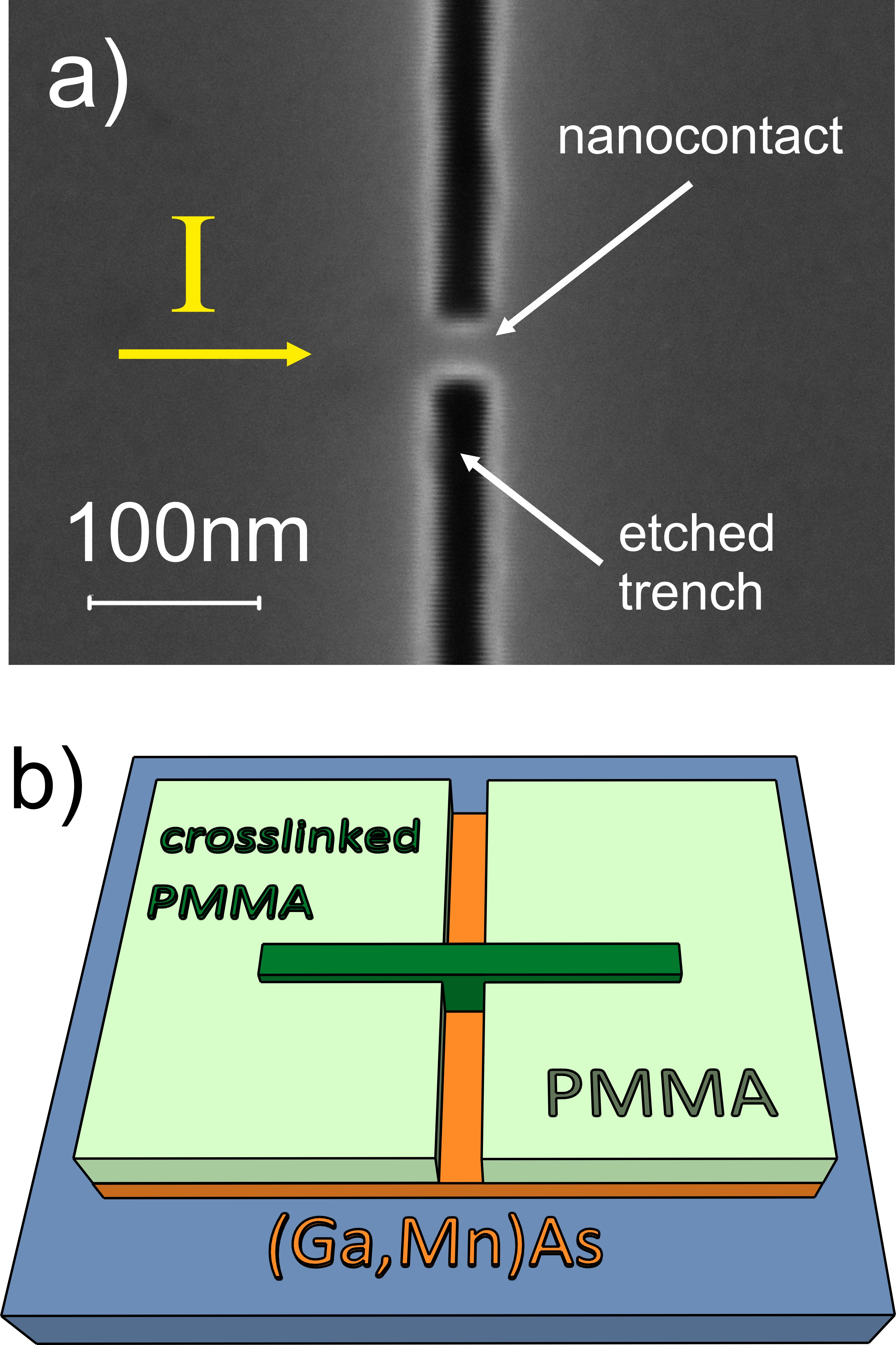
The structure of the PMMA mask, used for the two-step process, is sketched in Fig. 1a). It mainly consists of the crosslinked PMMA-line (dark green) of the first, high dose (30.000 C/cm) exposure step as well as of a narrow gap line from the second, usual exposure step, which separates the (Ga,Mn)As layer into two parts used as source- and drain-contacts. The two parts are connected with each other only at the NC, where the lines of the two exposure steps cross each other. This procedure allows us to define the width as well as the length of the NC by two single lines within independent exposure steps. This completely rules out the inter-proximity-effect between different exposed elements and reduces the minimum size of the NC to the smallest achievable linewidth of the two EBL steps. Compared to a single step process our approach is robust with respect to minor electron dose variations and thus well reproducible. Because of this, we were able to fabricate a large number of comparable devices and even to control the geometry of the NC with a precision of a few nanometers. Fig. 1b) shows an electron micrograph of the central part of a typical NC-device taken after the chemically assisted ion beam etching and resist removal using a low energy oxygen-plasma. After the nanopatterning we covered the whole sample with a thick -layer grown by a low temperature atomic layer deposition process at a temperature of C. The -layer acts on the one hand as the gate-dielectric and on the other hand it protects the tiny NC against oxidation. The top-gate contact was defined by optical lithography and covers not only the NC but also the center part of the whole device. It consists, similarly to the source- and drain-contacts, of a thick Ti/Au-stack evaporated thermally and structured using a standard lift-off technique.
An effective way to influence the transport behavior is to apply an annealing step after the nanopatterning. We used an annealing temperature of and durations from to . The post patterning annealing removes probably some of the defects induced by chemically assisted ion-beam etching. This can change an initially insulating sample to one in which Coulomb effects prevail or even to a conducting one. Annealing before the nanopatterning Schlapps et al. (2009); Edmonds et al. (2004), which removes defects induced during low temperature molecular beam epitaxy growth, is less effective than the post patterning annealing. Hence, the intrinsic structure of the NC is dominated by defects induced during the nanopatterning rather than by defects stemming from the low temperature molecular beam epitaxy growth.
III Measurement setup
All low temperature measurements presented in this work were carried out at a temperature of about using a -dilution fridge, equipped with a superconducting coil magnet. In combination with a rotatable sample holder, we were able to apply magnetic fields up to in any direction parallel to the sample plane. In order to saturate the magnetization of the device and to fix its direction, we applied a constant in-plane magnetic field with a magnitude of along one of the easy axes of the extended (Ga,Mn)As layer. This leads to a situation as sketched in Fig. 5a). The electrical transport experiments were carried out in a two terminal setup. We performed ac and dc measurements simultaneously by applying a dc bias-voltage modulated with a small oscillating ac component . The current flowing through the device was measured using a current amplifier which also converts the current into a corresponding voltage signal. The dc measurement using a digital multimeter provides the well known characteristic, while the ac measurement using a lock-in amplifier offers the differential conductance of the device. Our device could be tuned additionally by an external dc voltage () applied to the top-gate electrode of the device.
IV Experimental Results
IV.1 Room temperature properties
As mentioned in the introduction, all nanoconstricted (Ga,Mn)As-devices investigated in previous studies have shown a rather complex and irregular Coulomb diamond pattern Wunderlich et al. (2006); Schlapps et al. (2009). This has been explained by assuming that several metallic islands are involved in transport across the NC. Hence, shrinking the size of the NC should reduce the number of islands within the NC and bring up a more regular Coulomb diamond pattern. Looking for such samples, we investigated many different devices with widths and lengths of the NC ranging from to . Our experiments revealed that the transport properties of these devices are very sensitive to the width of the NC while its length has only a minor influence. Wider samples () show a mainly ohmic behavior while the most narrow ones () are fully insulating. Only samples with intermediate widths of show the typical SET-like behavior, discussed below. In many cases the room temperature resistance of the nanocontact already indicates whether the constriction is insulating, in the Coulomb blockade regime, or ohmic: For values (with the sheet resistance of k at 4.2 K) between 10 and 15 the constriction was in most cases in the Coulomb blockade regime for this specific material. However, similar to the earlier experiments, all of our SET-like samples, even the shortest and narrowest ones, have shown, on a first glance, an irregular Coulomb diamond pattern. Below we discuss in more detail transport in the Coulomb blockade regime.
IV.2 Coulomb blockade regime
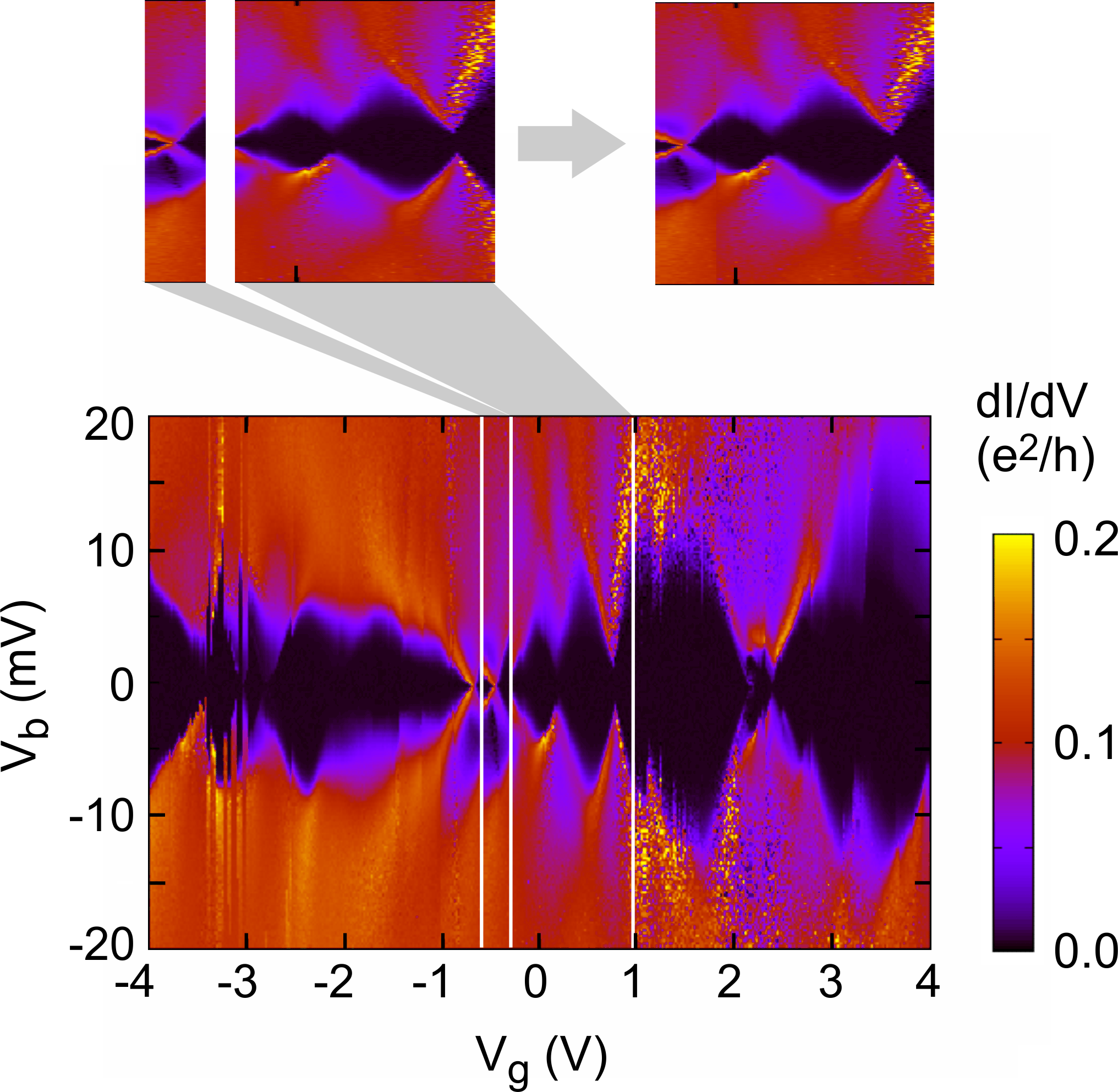
In Fig. 2 we present a highly resolved stability diagram of one of our NC-devices in the SET regime. The first impression is that the Coulomb diamond pattern is very irregular and exhibits frequent vertical discontinuities. Three of them are highlighted by white lines. These abrupt shifts can be assigned to charging or discharging of local traps in close vicinity to the NC, which, with their electrostatic potential, act as local gates. Their effect can thus be described as an abrupt jump along the gate voltage axis. This observation suggests a method to reconstruct the stability diagrams with unperturbed Coulomb diamonds. We cut the dataset in Fig. 2 along the white lines and shift the segments on the -axis until the diamonds fit onto each other. An example of this procedure is shown in the top inset of Fig. 2. In this way we obtain, for some parts of the -scale, Coulomb diamonds which are essentially cleared of potential jumps due to charge fluctuations in local traps. The dataset displayed in Fig. 3 has been reconstructed from the data shown in Fig. 2 and represents the starting point of our more detailed analysis.
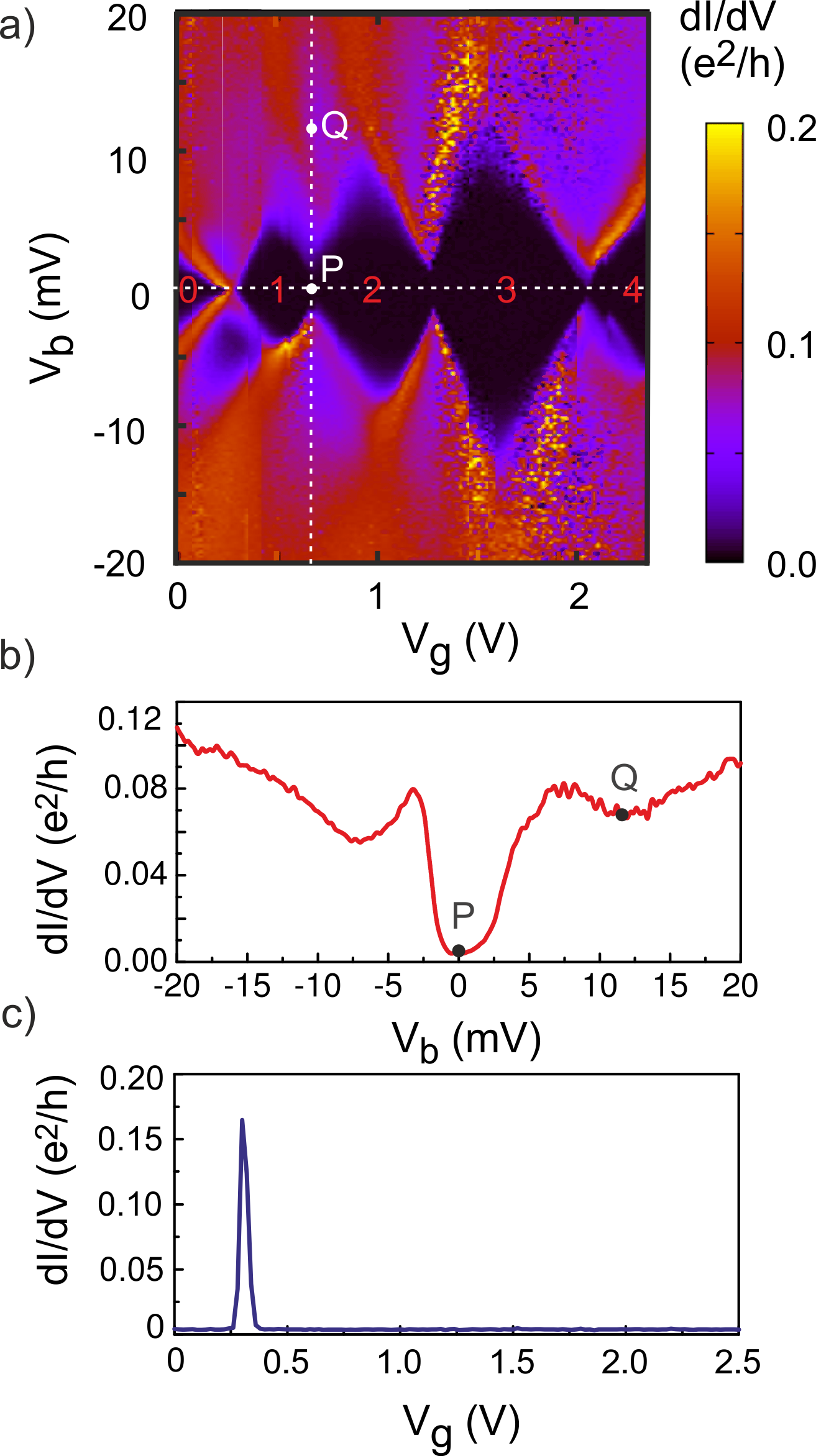
The stability diagram shown in Fig. 3 presents characteristic features typical for metallic single electron transistorsAverin and Likharev (1986, 1991); Grabert (1991); Grabert and Devoret (1992); Sohn et al. (1997) but also several anomalies. As expected, a series of diamonds of exponentially low differential conductance (black regions with fixed particle number) are surrounded by ridges of high conductance. Moreover, by further increasing the bias, the differential conductance does not drop to zero, see e.g. Fig. 3b), allowing to exclude the single particle energy quantization typical for quantum dots. Unexpectedly, though, i) the size and the shape of the Coulomb diamonds is not regular, ii) some of the diamonds are not closing at zero bias (e.g. corners between diamond 1 and 2 or between diamond 2 and 3 as seen from the gate trace in Fig. 3c)).
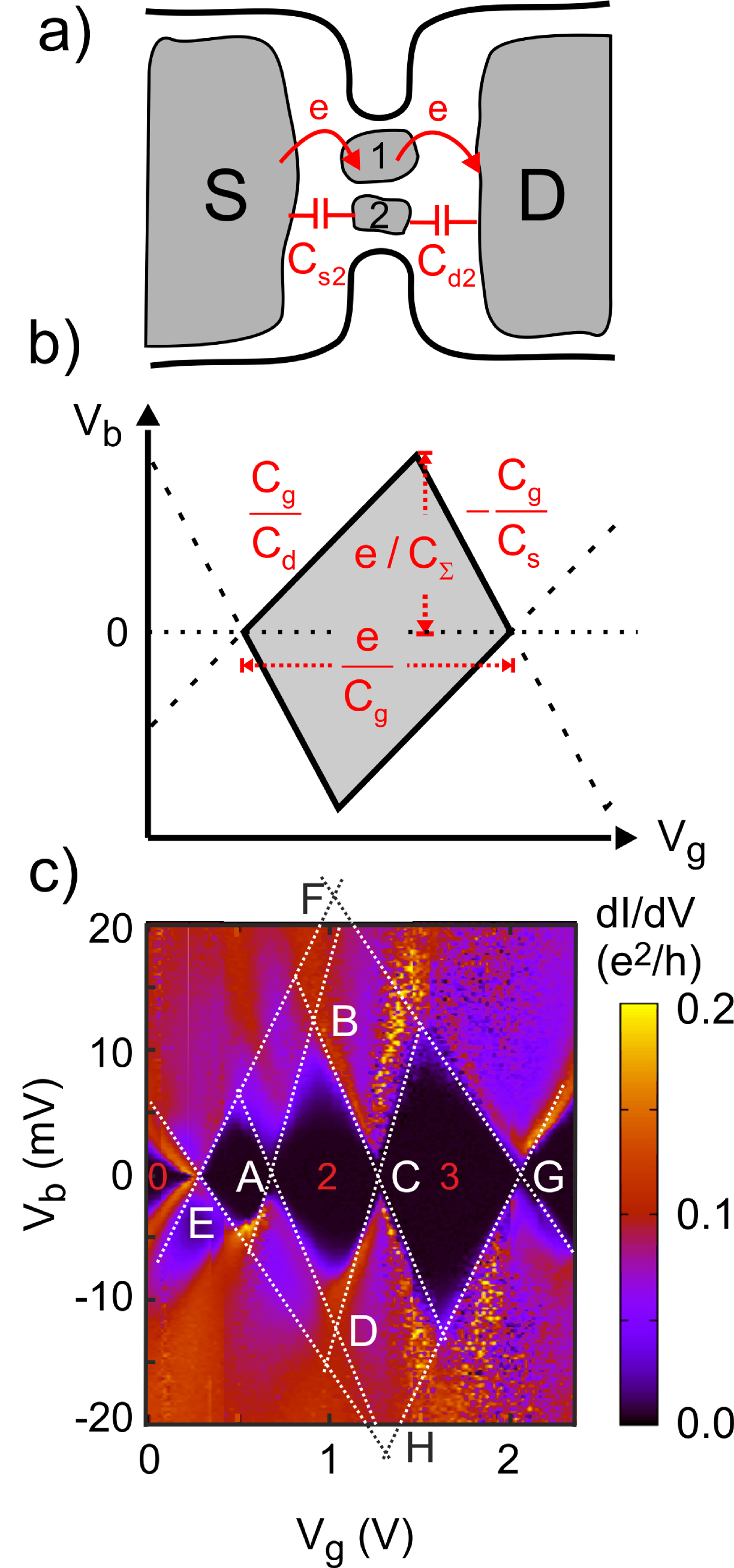
Concerning the first anomaly, it is striking that all the diamonds exhibit an individual height as well as an individual width. Additionally the diamond labeled 1 and the diamond labeled 3 are asymmetric: according to the classical orthodox theory Averin and Likharev (1986), one would expect that all Coulomb diamonds associated to a single island have the same size and shape, and that opposing edges of a Coulomb diamond were parallel. In the orthodox picture the two different slopes of a Coulomb diamond are related to the capacitive coupling of the island to the source- () and drain-leads (), as well as to the gate electrode (). Assuming , the slope of the source-line is given by while the slope of the drain-line is given by (see Fig. 4). In our case only the diamond numbered 2 has parallel source and drain lines. The diamonds labeled 1 and 3, however, exhibit four different slopes, so that we would extract from each two different values for and or two different values for , respectively. This suggests that our NC consists actually of two metallic islands producing a set of nested diamonds.
Fig. 4a) shows a simple schematic to illustrate our interpretation: the two islands are arranged in parallel, so that an electron can tunnel from the source-lead directly to each of the two islands and from there in a subsequent tunneling process directly to the drain-lead. By taking into account the slopes of the diamond edges as well as the distance between neighboring charge degeneracy points we can obtain two different sets of parameters (, , ) from our experimental data. Each set of parameters characterizes one of the two islands. One set can be extracted from the regularly shaped diamond 2. For the other one, we have to reconstruct a second regular Coulomb diamond by extending the outer edges of diamond 1 and 3 until they cross each other, see Fig. 4c). The extracted parameters are summarized in Table 1. Our analysis is limited to certain gate voltage ranges. We attribute this limitation to possible differences in the shape and even in the number of participating island associated to different gate voltage regions. Nevertheless, the simple orthodox model gives already a satisfactory agreement between experimental and theoretical -stability diagrams and suggests that transport, in this gate voltage range, occurs primarily in parallel across two islands of different size in the reconstructed gate voltage segments. However, the model presented so far can not account for the second anomaly, i.e. a pronounced transport blocking observed in the vicinity of the charge degeneracy point between the diamonds 1-2 and 2-3, see also Fig. 2b). On the other hand, the gap is not present at the charge degeneracy point 0-1 and is barely visible at 3-4, see also Fig. 3c). Hence, the gap is assigned to the island with the smaller charging energy. In order to account for this experimental observation, we resort below to a more sophisticated transport model that includes the ferromagnetic nature of the material.
| small CD (ABCD) | large CD (EFGH) | |
|---|---|---|
V Theoretical modeling
In this section we extend the orthodox theory of Coulomb blockade Averin and Likharev (1986, 1991); Grabert (1991); Grabert and Devoret (1992); Sohn et al. (1997) in order to account for the ferromagnetic properties of the (Ga,Mn)As samples. Although transport through magnetic islands has been addressed in the literature, Barnaś and Weymann (2008) scarce consideration has been given, to our knowledge, to the role played by an energy dependent density of states in the metallic islands. The latter, instead, is crucial to explain the anomalous current blocking observed in the present experiment.
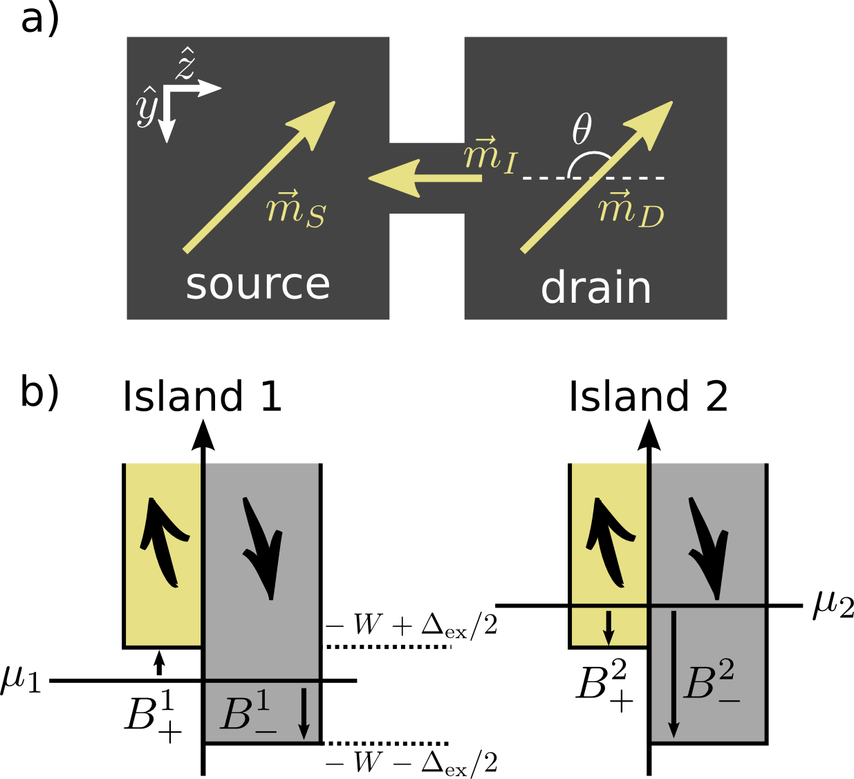
To this end we assume that both leads and the metallic islands are spin polarized. Fig. 5a) shows a sketch of the magnetization directions expected in the experiments. The magnetization of the ferromagnetic (Ga,Mn)As leads is rather weak, and can be tuned by an external magnetic field. It forms in our experiment an angle of (easy direction) with the transport direction, set by the longitudinal axis of the NC (-axis, cf. Fig. 5a)). In the constriction, however, the spin polarization axis is strongly influenced by strain effects and is expected to be along the NC longitudinal axis.
In order to explain the blockade effects we claim that the angle between the leads and the constrictions magnetization lies in the range . In other words current suppression originates from the fact, that the majority spin carriers in the islands and in the leads have effectively the opposite polarization. Since only one of the two superimposed Coulomb diamond structures shows a noteworthy blockade effect, we conclude, within our model, that the structure with the blockade stems from transport through a fully polarized island, while the second island is only partially polarized.
We describe the islands polarization with an upward shift in energy of the minority spin band with respect to the majority spin band, see Fig. 5b). The electro-chemical potential is the external parameter which determines whether the island is partially or fully polarized. Partial polarization is obtained if the chemical potential () lies above the bottom of the minority spin band, full polarization when the chemical potential lies between the bottom of the majority and of the minority spin bands.
In our model the tunneling of a source electron of the majority spin species (conventionally the spin up) to a fully down polarized island is highly suppressed for low bias voltages since no spin up states are available near the Fermi level. For bias voltages which are large enough to access also the minority spin band (, cf. Fig. 5b)), the suppression is lifted and an increase of the current is expected. For the partially polarized island both spin species can be accessed already at the Fermi energy and no suppression is observed.
V.1 Model Hamiltonian
We describe the nanoconstriction with a system-bath model aimed at mimicking the structure of the two islands contacted to source and drain leads sketched in Fig. 4a). The total Hamiltonian is
| (1) |
where
| (2) |
denotes the Hamiltonian of the two spin polarized leads. We assume to have a flat, but spin dependent, density of states ()
| (3) |
which depends on the polarization of the leads (). The metallic islands () in the nanoconstriction are modeled by
| (4) |
and have in general a different spin quantization axis as the contacts. We define for spin , respectively, using the spin-quantization axis of the nanoconstriction. As already mentioned, we account for the ferromagnetic properties of the metallic islands by assigning spin dependent energy levels, , and consequently a relative shift of the density of states for the two spin directions, (Fig. 5b)). The long range Coulomb interactions are included within a constant interaction model, where is the charging energy of the island . The effective coupling of the gate electrode to the metallic islands is taken into account by the term proportional to , with being an effective gate coupling parameter and the gate voltage. The two metallic islands and the leads are weakly coupled by the tunneling Hamiltonian
| (5) |
where we defined the function , . It results from the non-collinear spin quantization axis of the islands and the leads. Since the two axis are rotated by an angle of in the --plane with respect to each other, the transformation conserves the spin during tunneling.
V.2 Density of states of the metallic islands
Some of the experimental observations can only be understood if the energy dependence of the density of states, in particular the presence of different band edges for minority and majority spins, is accounted for. Specifically, we define the spin-dependent density of states of island as:
| (6) |
where is the spin independent contribution to the bandwidth, and the exchange band splitting of the ferromagnetic metallic island. The parameter defines the strength of the density of sates. Since the is the largest energy scale considered in the following, the upper limit of the density of states can be set to infinity. In the last line of Eq. (6) we have approximated the left Heaviside function by , with the Fermi function; this allows us to further proceed analytically in the calculation of the transport properties. The density of states is also sketched for clarity in Fig. 5b). For later reference we define as the energy difference between the bottom of the band of the corresponding spin species and the chemical potential of the island : .
V.3 Transport theory
In the following we briefly outline the main steps leading to the evaluation of the transport characteristics, emphasizing the new ingredients entering our transport theory. For more details we refer to the Appendix B. The framework is the orthodox theory of Coulomb blockade Averin and Likharev (1986, 1991); Grabert (1991); Grabert and Devoret (1992); Sohn et al. (1997), extended to the case of ferromagnetic contacts Barnaś and Weymann (2008) and valid also for fully spin polarized metallic islands. The explicit derivation of the tunnelling rates should illustrate the crucial role played in our theory by the energy dependent density of states.
The theory is based on a master equation for the reduced density matrix of the islands, up to second order in the tunneling Hamiltonian. Since the two metallic islands are assumed not to interact with each other, the corresponding density matrices obey independent equations of motion (see Appendix B). Moreover, the metallic islands are assumed large enough to posses a quasi continuous single-particle spectrum, but small enough that their charging energy dominates the tunnelling processes that change their particle number. We further assume that, in between two tunnelling events, the islands relax to a local thermal equilibrium. Under these assumptions the reduced density matrix of island can be written as
| (7) |
where is the part of the system Hamiltonian associated to the island , is the projection operator on the -particle subspace and is the corresponding (canonical) partition function. By projecting the master equation on the -particle subspace and tracing over the islands degrees of freedom, we keep only the occupation probabilities of finding the island occupied by electrons as dynamical variables. In the stationary limit we find (see Appendix B)
| (8) |
Eventually, the stationary current through lead reads
| (9) |
In Eqs. (8) and (9) the rates are defined as
| (10) |
and are expressed in terms of the normal state resistance and the functions and , with the inverse temperature. We account for the asymmetric bias drop with the bias coupling constants defined as . Further, we defined the grand canonical addition energy
| (11) |
which must be paid in order to increase the electron number on island from . We denote the chemical potential of the leads at bias .
The rates given in Eq. (10) differ from the ones of the orthodox theory of Coulomb Blockade Averin and Likharev (1986, 1991); Grabert (1991); Grabert and Devoret (1992); Sohn et al. (1997) even in their spin dependent variation Barnaś and Weymann (2008) due to the energy dependent density of states and the explicit dependence on the band edges. The latter introduce a new source of current suppression associated to the absence of states with a specific spin species. These rates represent the main theoretical contribution of the present work. For the chemical potential lying far above the bottom of the bands, the theory recovers again the limit of the classical orthodox theory of Coulomb blockade. Namely, in the limit :
| (12) |
VI Theoretical Results
VI.1 Comparison with the experiments
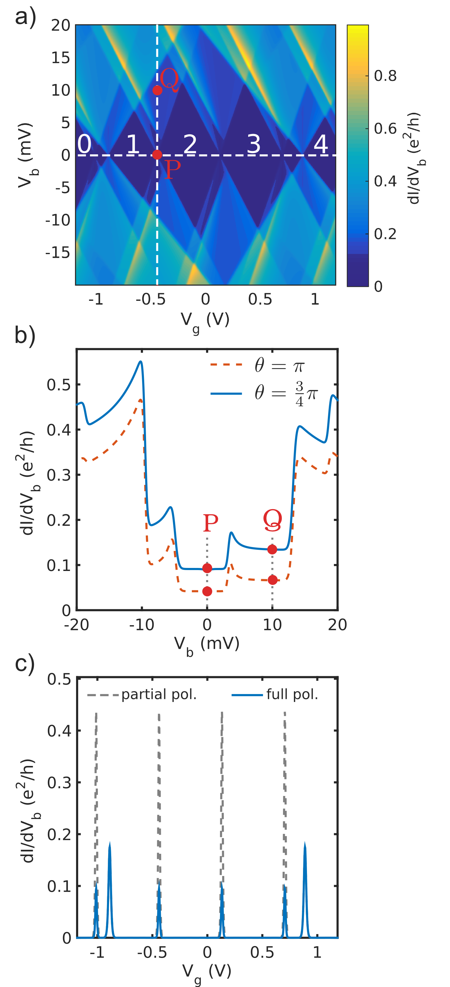
The results of our simulation are reported in Fig. 6a), with the differential conductance shown as a function of the bias and gate voltage. We see the same nested diamond structure as in the experiments. In our theory the diamonds at the charge degeneracy points labeled 0-1 and 3-4 close. Between the diamonds 1-2 and 2-3 the differential conductance is suppressed for bias voltages smaller than a certain threshold bias. Fig. 6b) shows a bias trace calculated at the charge degeneracy point 1-2, for two different angles between the magnetization vectors of the leads, , and the metallic islands, . It shows a suppression of the differential conductance at point (P) with respect to point (Q). The width of the suppression region corresponds to the one observed experimentally in Fig. 3b) and is proportional to , the energy difference between the bottom of the minority spin band and the chemical potential of island (cf. Fig. 5b)). In contrast to the experiments no full blockade can be observed at (P). A change of the orientation of the magnetization directions from (dashed red line) to (solid blue line) is shifting the curve upwards. Besides the constant shift the two curves are qualitatively the same.
To emphasize the effect of the islands degree of polarization on the suppression mechanism, a conductance trace at of a full polarized island is compared to the case of a partial polarized island in Fig. 6c). Partial polarization is achieved by shifting the electrochemical potential of island by meV up in energy. The solid blue line shows the full polarized case, where the two larger peaks correspond to the larger Coulomb diamond (island ). The peak observed in the experiment (Fig. 3c)) we ascribe to transport across this partially polarized island. Although the theoretically predicted second peak is missing in Fig. 3c) we note that the corresponding blockade between diamond 3 and 4 is much less pronounced than between, e.g. 2 and 3. This asymmetry between the degeneracy points 0-1 and 3-4, however, cannot be accounted for by our model which predicts a periodicity of the Coulomb oscillation pattern. The four smaller peaks in Fig. 6c) belong to the smaller Coulomb diamond structure, corresponding to island , i.e. the fully polarized one (Fig. 5b)). Even though the conductance is not completely suppressed as in the experiment, the conductance peaks are strongly reduced with respect to the partially polarized case. In the latter (dashed grey lines) no suppression is present and the conductance peaks of island are by a factor of larger. Below we address a possible reason for the incomplete blocking within the model. Since the parameters of island are kept the same, both for the fully and partially polarized cases the corresponding conductance peaks are not changing. Despite the fact that a comparison of the calculated gate trace to the experimental one in Fig. 3c) reveals some limitations of the model, the essential feature, i.e. the suppression inside the large Coulomb diamond, is reproduced.
VI.2 The mechanism of current suppression
For a better understanding of the mechanism underlying the blockade, we derive analytically the differential conductance for the island at the two points (P) and (Q) marked in Fig. 6b). For simplicity the case is considered, since qualitatively the blockade mechanism is the same in both cases.
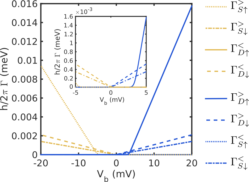
Notice that both P and Q correspond to a gate voltage such that , i.e. at the charge degeneracy point of the - transition. To obtain the differential conductance, according to Eq. (8) and (9), the transition rates are required. For simplicity we have dropped the subscript from the excitation energy since we will refer from now on always to the same island.
In Fig. 7 we show the transition rates as a function of the bias . To simplify the notation, we replaced . Notice their linear dependence on the bias above a certain threshold. Thus, in that bias range one can approximate them as:
| (13) |
where is a constant accounting for the threshold bias, and
| (14) |
Here, is assumed to be independent of the lead. For the point (P) within the first plateau only the rates with , namely and , are nonzero. Hence, according to the principle of detailed balance: . Imposing probability conservation we find . Thus the stationary current equals , which is suppressed for a large spin polarization . Here the polarization is assumed to be equal for both leads.
At the point (Q), only one additional rate, , is contributing (the rate is zero due to the lower bound of the density of states). In this bias range the equations of detailed balance and probability conservation yield The resulting stationary current is then Again the current is suppressed for large spin polarization.
Taking the ratio of the two differential conductance plateaus, i.e. the ratio of Eqs. (43) and (44), we find
| (17) |
Thus, within our simple model, the ratio of the height of the two plateaus is limited by
| (18) |
In other words the ratio of the two differential conductance plateaus is limited in our theory, leading to some discrepancy with the experimentally observed ratio, cf. points (P) and (Q) marked in Fig. 3b). Since the parameters are determined experimentally, the only possibility to change the ratio is to modify the coupling constants . However, the increase of the coupling constants necessary to fit the experimental value, would lead to a huge asymmetry in the stability diagram which is not observed experimentally. Despite the discrepancy between and the experimental ratio, we think that the theory clearly suggests a mechanism which can lead to a suppression of the conductance due to spin polarization in the framework of an orthodox theory of Coulomb blockade. To better fit the experiments a more realistic energy dependence of the density of states which also accounts for valence bands is necessary. With such an energy dependence the rates can change their slope as a function of the bias voltage, leading to an even more pronounced bias dependent suppression of the differential conductance.
VII Conclusion
In this work we have reported on a detailed study of the transport characteristics of nanofabricated narrow constrictions in (Ga,Mn)As thin films. By means of a two step electron beam lithography technique we have fabricated well defined nanoconstrictions of different sizes. Depending on channel width and length, for a specific material, different low-temperature transport regimes have been identified, namely the ohmic regime, the single electron tunnelling regime (SET) and a completely insulating regime. In the SET, complex stability diagrams with nested Coulomb diamonds and anomalous conductance suppression in the vicinity of charge degeneracy points have been measured.
In order to rationalize these observations we proposed, for a specific nanoconstriction, a model consisting of two ferromagnetic islands coupled to ferromagnetic leads. In particular, the angle between the leads and the islands magnetization lies in the range . Moreover, the full polarization of one of the metallic islands is crucial. We studied the transport characteristics of the system in terms of a modified orthodox theory of Coulomb blockade which takes into account the energy dependence of the density of states in the metallic islands. The latter represents an important generalization of existing formulations and is determinant for the qualitative understanding of the present experiments. In fact, the explicit appearance of the minority spin band edge in the expression of the tunnelling rates yields a pronounced conductance suppression at the charge degeneracy points. To account for the full suppression of conductance observed in the experiments the simple model used in this work should be further improved. For example the hole character of the charge carriers and associated spin orbit coupling effects are not captured by our model. Furthermore, it is straightforward to combine the present theory with microscopic models that allow for a realistic description of the islands density of states.
We acknowledge for this work the financial support of the Deutsche Forschungsgemeinschaft under the research programs SFB 631 and SFB 689.
Appendix A Sample fabrication
A.1 Two-step EBL fabrication process
Both steps are based on the standard EBL resist poly-methyl-methacrylate (PMMA). In the first step one exposes the resist using an extremely high line-dose (approx. ) in order to define a narrow crosslinked PMMA-line. This line is very robust and does not get removed by common organic solvents like acetone. Hence, after cleaning the sample in a bath of acetone, the crosslinked PMMA-line remains on top of the sample while the unexposed PMMA is removed from the sample surface. For the second step the sample is again coated with a fresh layer of PMMA resist. This time one uses a common dose (approx. ) in order to expose a second line perpendicular to the crosslinked one. After removing the exposed resist using a standard developer solution consisting of isopropyl alcohol and Methyl-isobutyl-ketone (MIBK), we get the patterned mask for the subsequent ion-beam-etching, shown in Fig. 1a).
Appendix B Equation of motion for a orthodox theory of Coulomb blockade
In this appendix we derive an extension of the orthodox theory of Coulomb blockade for the case of spin polarized contacts as well as of a spin polarized metallic island. In particular we will consider explicitly the lower bound of the density of states in the metallic island.
The transport theory is based on the Liouville-von Neumann equation for the reduced density matrix in the interaction picture
| (19) |
which we expand to second order in the tunneling Hamiltonian . Prior to the system and the leads do not interact and the density matrix can be written as a tensor product of the density matrices of the subsystems
| (20) |
Since the leads are considered thermal baths of noninteracting fermions, reads
| (21) |
Further, we assume that due to fast relaxation processes in the leads, the density matrix can be written as , with . Moreover, due to the independence of the two metallic islands and each component obeys the following equation of motion:
| (22) |
where labels the metallic island.
For the system we assume that the metallic islands are large enough to posses a quasi continuous single-particle spectrum, but small enough that their charging energy dominates the tunnelling processes that change their particle number. Furthermore, it is assumed that the islands will relax to a local thermal equilibrium on a time scale shorter than the inverse of the average electronic tunnelling rate. Under these assumptions, the reduced density matrix can be written as
| (23) |
with , and
| (24) |
is the projection operator on the -particle subspace. Notice that in Eq. (23), due to the projector operator , the only statistically relevant term of the system Hamiltonian is . The term becomes a constant and is canceling out in the density matrix. Inserting explicitly in Eq. (22), we find
| (25) |
In the following we are analyzing the first term of Eq.(25) in more detail, the other terms can be evaluated in complete analogy. The calculation of the trace over the lead degrees of freedom gives
| (26) |
where the time evolution of the creation and annihilation operators of the leads is given by . For the system operators the time evolution can be carried out in a similar way, keeping in mind that the parts proportional to the total number operator can be factorized
| (27) |
In order to perform the trace over the system degrees of freedom another approximation is necessary. By taking the average in the grand canonical ensemble, the particle number is determined by the chemical potential and we can remove the projection operator:
| (28) |
This approximation becomes exact in the limit of . In presence of a quasi-continuous energy spectrum of the islands we can further drop the dependence of the chemical potential, for small relative variations of .
The trace in Eq. (27) can now be evaluated in the standard way and it yields Fermi functions. Inserting the results for the traces in Eq. (25) we obtain:
| (29) |
Since we are only interested in the stationary solution of the master equation, we send and use the Dirac identity
| (30) |
to evaluate the integrals. Due to statistical averages no coherences are possible in the master equation and the two complex conjugated parts can be summed up. We find
| (31) |
Further, we consider the continuum limit of the states in the quantum dot
| (32) |
with being the energy dependent density of states in island with the spin , defined in Eq. (6). For the leads
| (33) |
where is the density of states of lead which is considered in the flat band limit. The integration over the lead degrees of freedom gives:
| (34) |
where . In a last step we insert , see Eq. (6) in the main text, and the remaining integral can be done by using the following identities:
| (35) |
| (36) |
| (37) |
and are defined in the main text just below Eq. (10). Using these identities yields the final result
| (38) |
Appendix C Current
Finally we briefly outline the derivation of the current formula. The current is defined as
| (39) |
In the interaction picture the total particle number operator of lead , , is not evolving in time since it commutes with the unperturbed part of the Hamiltonian. Therefore, the current reads
| (40) |
where we expand up to second order in . The first term of Eq. (40) vanishes since only a odd number of operators appear in the trace. In the second term we replace . Exploiting further the cyclic invariance of the trace we find
| (41) |
In the last step we exploited the anti-hermiticity of . Following the same steps as in the derivation of the master equation, one can identify the rates, and one finds the well known expression of the current
| (42) |
Appendix D Calculation of the differential conductance
Differentiating Eq. (15) with respect to and inserting the definition of Eq. (14) yields the differential conductance of the first plateau:
| (43) |
To calculate the differential conductance at this point we differentiate Eq. (16) with respect the bias voltage and find
| (44) |
where we defined , , , and . In order to find the value of the differential conductance plateau we have to consider the high bias limit and we find
| (45) |
Inserting back the physical constants we find
| (46) |
References
- Ohno et al. (1996) H. Ohno, A. Shen, F. Matsukura, A. Oiwa, A. Endo, S. Katsumoto, and Y. Iye, Applied Physics Letters 69, 363 (1996).
- Dietl and Ohno (2014) T. Dietl and H. Ohno, Rev. Mod. Phys. 86, 187 (2014).
- Jungwirth et al. (2006) T. Jungwirth, J. Sinova, J. Mašek, J. Kučera, and A. H. MacDonald, Rev. Mod. Phys. 78, 809 (2006).
- Sato et al. (2010) K. Sato, L. Bergqvist, J. Kudrnovský, P. H. Dederichs, O. Eriksson, I. Turek, B. Sanyal, G. Bouzerar, H. Katayama-Yoshida, V. A. Dinh, et al., Rev. Mod. Phys. 82, 1633 (2010).
- Rüster et al. (2003) C. Rüster, T. Borzenko, C. Gould, G. Schmidt, L. Molenkamp, X. Liu, T. Wojtowicz, J. Furdyna, Z. Yu, and M. Flatté, Phys. Rev. Lett. 91, 216602 (2003).
- Giddings et al. (2005) A. Giddings, M. Khalid, T. Jungwirth, J. Wunderlich, S. Yasin, R. Campion, K. Edmonds, J. Sinova, K. Ito, K.-Y. Wang, et al., Phys. Rev. Lett. 94 (2005).
- Schlapps et al. (2006) M. Schlapps, M. Doeppe, K. Wagner, M. Reinwald, W. Wegscheider, and D. Weiss, physica status solidi (a) 203, 3597 (2006), ISSN 1862-6319.
- Ciorga et al. (2007) M. Ciorga, M. Schlapps, A. Einwanger, S. Geissler, J. Sadowski, W. Wegscheider, and D. Weiss, New J. Phys. 9, 351 (2007).
- Pappert et al. (2007) K. Pappert, S. Huempfner, C. Gould, J. Wenisch, K. Brunner, G. Schmidt, and L. W. Molenkamp, Nature Physics 3, 573 (2007).
- Wunderlich et al. (2006) J. Wunderlich, T. Jungwirth, B. Kaestner, A. Irvine, A. Shick, N. Stone, K.-Y. Wang, U. Rana, A. Giddings, C. Foxon, et al., Phys. Rev. Lett. 97 (2006).
- Schlapps et al. (2009) M. Schlapps, T. Lermer, S. Geissler, D. Neumaier, J. Sadowski, D. Schuh, W. Wegscheider, and D. Weiss, Phys. Rev. B 80, 125330 (2009).
- Averin and Likharev (1986) D. V. Averin and K. Likharev, J. Low Temp. Phys. p. 345 (1986).
- Averin and Likharev (1991) D. V. Averin and K. K. Likharev, Mesoscopic Phenomena in Solids (Elsevier Science, Amsterdam, 1991).
- Grabert (1991) H. Grabert, Zeitschrift Für Phys. B Condens. Matter 85, 319 (1991).
- Grabert and Devoret (1992) H. Grabert and M. H. Devoret, eds., Sigle Charge Tunneling, NATO ASI Series (Springer US, 1992).
- Sohn et al. (1997) L. Sohn, L. Kouwenhoven, and G. Schön, eds., Mesoscopic Electron Transport, NATO ASI Series (Kluwer, 1997).
- Barnaś and Weymann (2008) J. Barnaś and I. Weymann, J. Phys.: Condens. Matter 20, 423202 (2008).
- Edmonds et al. (2004) K. Edmonds, P. Boguslawski, K. Wang, R. Campion, S. Novikov, N. Farley, B. Gallagher, C. Foxon, M. Sawicki, T. Dietl, et al., Phys. Rev. Lett. 92, 037201 (2004).