A Novel Architecture of Area Efficient FFT Algorithm for FPGA Implementation
Abstract
Fast Fourier transform (FFT) of large number of samples requires huge hardware resources of field programmable gate arrays (FPGA), which needs more area and power. In this paper, we present an area efficient architecture of FFT processor that reuses the butterfly elements several times. The FFT processor is simulated using VHDL and the results are validated on a Virtex-6 FPGA. The proposed architecture outperforms the conventional architecture of a -point FFT processor in terms of area which is reduced by a factor of with negligible increase in processing time.
Index Terms:
FFT, FPGA, Resource optimizationI Introduction
Field programmable gate arrays (FPGA) are programmed specifically for the problem to be solved, hence they can achieve higher performance with lower power consumption than general purpose processors. Therefore, FPGA is a promising implementation technology for computationally intensive applications such as signal, image, and network processing tasks [1].
Fast Fourier transform (FFT) is one of the most widely used operation in digital signal processing algorithms [2] and plays a significant role in numerous signal processing applications, such as image processing, speech processing, software defined radio etc. FFT processors should be of higher throughput with lower computation time. So, for computing larger number of data samples, we have to think about the area of the FFT processor since the number of stage of FFT computation increases with a factor of . In the design of high throughput FFT architectures, energy-efficient design techniques can be used to maximize performance under power dissipation constraints.
Spatial and parallel FFT architecture, also known as array architecture [3], based on the Cooley-Tukey algorithm layout, is one of the potential high throughput designs. However, the implementation of the array architecture is hardware intensive. It achieves high performance by using spatial parallelism, while requiring more routing resources. However, as the problem size grows, unfolding the architecture spatially is not feasible due to serious power and area issue arisen by complex interconnections.
The pipelined architectures are useful for FFTs that require high data throughput [4, 5, 6, 7]. The basic principle of pipelined architectures is to collapse the rows. Radix-2 multi-path delay commutator [8] [9] was probably the most classical approach for pipeline implementation of radix-2 FFT algorithm. Disadvantages include an increase in area due to the addition of memories and delay which is related to the memory usage [10].
In this paper, we propose a novel architecture of area efficient FFT by reusing numbers of butterfly units more than once instead of using butterfly units once [11]. This is achieved by a time control unit which sends back the previously computed data of butterfly units to itself for times and reuses the butterfly units to complete FFT computation. The area requirement is obviously smaller, only radix- elements, than the array architecture and pipelined architectures, being the number of sample points.
II Traditional FFT Algorithm
The Cooley-Tukey FFT algorithm is the most common algorithm for developing FFT. This algorithm uses a recursive way of solving FFT of any arbitrary size . The technique divides the larger FFT into smaller FFTs which subsequently reduce the complexity of the algorithm. If the size of the FFT is then this algorithm makes where and are sizes of the smaller FFTs. Radix-2 decimation-in-time (DIT) is the most common form of the Cooley-Tukey algorithm, for any arbitrary size . can be expressed as a power of 2, that is, , where is an integer. This algorithm is called decimation-in-time since at each stage, the input sequence is divided into smaller sequences, i.e. the input sequences are decimated at each stage. A FFT of -point discrete-time complex sequence , indexed by is defined as:
| (1) |
where . Radix-2 divides the FFT into two equal parts. The first part calculates the Fourier transform of the even index numbers. The other part calculates the Fourier transform of the odd index numbers and then finally merges them to get the Fourier transform for the whole sequence.
Seperating the into odd and even indexed values of , we obtain
| (2) |
III Proposed FFT Algorithm
The area of a FFT processor depends on the total number of butterfly units used. Each butterfly unit consists of multiplier and adder/subtractor blocks. Higher the bit resolution of samples, larger the area of these two mathematical blocks. According to traditional FFT algorithm each stage contains numbers of butterfly units. Therefore, for a traditional FFT processor, the total number of butterfly units is given by
| (3) |
In the proposed algorithm, number of butterfly units are reused for times. Therefore, the modified architecture of FFT processor requires number butterfly units which is given by
| (4) |
.
The proposed architecture of FFT processor reduces the number of butterfly units by a factor of (), which is given by
|
|
(5) |
.
Table I shows that the number of multipliers and adders/subtractors for the proposed FFT is less compared to that of the traditional FFT.
| Traditional FFT | Proposed FFT | |
|---|---|---|
| Butterfly unit (BU) | ||
| Multiplier | ||
| Adder/subtractor |
| Number of samples | Traditional | Proposed |
|---|---|---|
| architecture | architecture | |
| 8 | 12 | 4 |
| 16 | 32 | 8 |
| 32 | 80 | 16 |
| 64 | 192 | 32 |
| 128 | 448 | 64 |
| 256 | 1024 | 128 |
| 512 | 2304 | 256 |
| 1024 | 5120 | 512 |
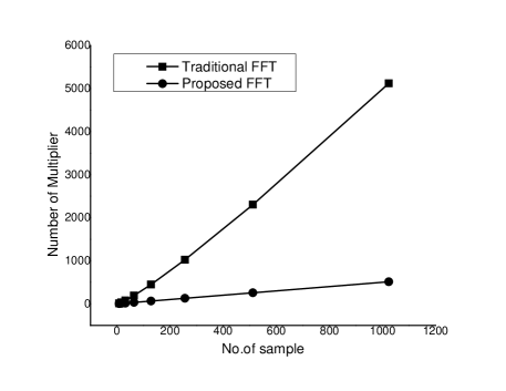
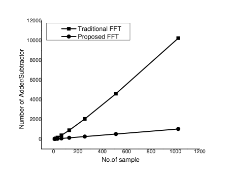
IV Architecture of Proposed FFT Processor
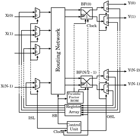
The key feature of the proposed FFT processor is its low area. The proposed architecture reuses number of butterfly units for times. Block diagram of overall architecture of proposed FFT processor are shown in Fig.3. It consists of routing network, butterfly unit, control unit and input output enable blocks.
IV-A The control unit
Here the control unit is used for syncronizing all the blocks of the FFT processor. It counts the number of stage and controls the input, output and feedback databus. The control block generates three signals 1bit Input Select Line (ISL), output select line (OSL) and multi-bit stage bus (SB). This stage bus (SB) contains the stage of FFT computation. The control unit increments the number of stage with the rising edge of the clock signal. at initial stage to select data from extarnal source after that to select data from the feedback path or register array for times and for times to fetch the output data of the butterfly unit to register array. At th time to enable the output data path of the FFT processor.
IV-B Butterfly unit (BU)
From the mathematical diagram, the output samples of the butterfly unit is generated after addition and subtraction operation with the product of even data sample and twiddle factor as shown in Fig.4.

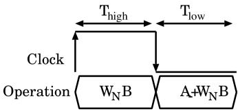
These butterfly units are clock capable. The multiplication operation starts with the rising edge of the clock and addition or subtraction operation is done with the falling edge of the clock signal. So, that total operation of the butterfly unit is done within a single clock cycle as shown in Fig.5.
IV-C Twiddle factor ROM
The twiddle factor ROM stores the twiddle factor co-efficients. Size of this ROM unit is . This block have number of output signal which are connected with number of butterfly unit. The stage bus (SB) is connected with the address bus of ROM.
IV-D Routing network and register array
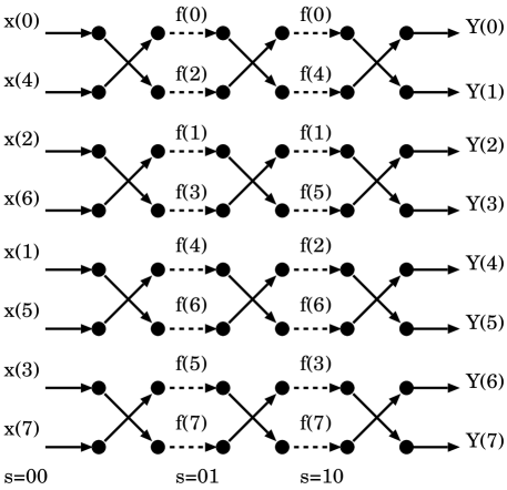
Routing network unit passes the proper sequences of input samples to the butterfly units for different stage of computations. Value of stage bus (SB) controls output of this unit. At first stage, routing network generates bit-reversed sample sequence of input samples. For the remain stages, the routing network shuffles the feedback samples with distance of where . Figure.6 shows the data path layout of 8-point FFT. Dashed arrows define the feedback samples. Cross arrows signifies the butterfly units. Register array [12] holds the previous data of the butterfly units and passes the stored data with the rising edge of the clock.
V Implementation and Results
Figure 7 shows the architecture of 8-point FFT processor according to proposed FFT processor. Figure.8 shows the timming diagram of this processor. and denotes input and output samples and are the ouput samples of previous stage.


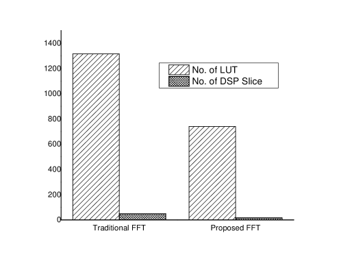
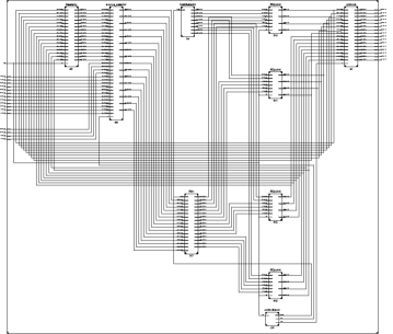
The proposed architecture for 8-point FFT processor is coded using VHDL, emulated and synthesized using Xilinx ISE 14.2 for Virtex-6 FPGA. Table.III shows the comparison of advanced HDL synthesis reports with traditional FFT. Figure.10 shows the generated detailed RTL diagram of proposed 8-point FFT processor. Figure.9 shows the comparison of number of DSP slices and LUTs requirements and Table.IV shows the comparison of timming delay with the traditional FFT processor.
| Hardware | Traditional FFT | Proposed FFT |
|---|---|---|
| MACs | 24 | 8 |
| Multipliers | 24 | 8 |
| Adder/Subtractors | 72 | 25 |
| Multiplexers | 360 | 136 |
| XORs | 24 | 8 |
| Registers | – | 288 |
| counter | – | 1 |
| Algorithm | Delay (nsec) |
|---|---|
| Traditional FFT | 29.111 |
| Proposed FFT | 29.397 |
| Device Utilization Summary | |
|---|---|
| Selected Device | 6vsx475tff1759-2 |
| Number of Slice Registers | 301 out of 595200 |
| Number of Slice LUTs | 748 out of 297600 |
| Number of DSP48E1s | 16 out of 2016 |
| Timing Summary | |
| Minimum period | 19.598ns |
| Maximum Frequency | 51.025MHz |
| Minimum input arrival | 9.384ns |
| time before clock | |
| Maximum output required | 0.665ns |
| time after clock | |
VI Conclusion
The proposed architecture presents an area efficient Radix-2 FFT processor. The algorithm reuses the butterfly units of single stage more than once which reduces the area drastically. The architecture has been emulated and the performance analysis has been carried out in terms of overall response time and utilization of hardware resources of FPGA. Detailed analysis reveals that the proposed architecture reduces the area dramatically without compromising the response time. Further improvements may be obtained by designing silicon layout and analysing the post-layout performance trade-off.
References
- [1] G. Nordin, P. Milder, J. Hoe and M. Puschel, Automatic generation of customized discrete Fourier transform IPs, Design Automation Conference, 2005. Proceedings. 42nd, 2005, pp. 471–474.
- [2] B. M. Baas, A low-power, high-performance, 1024-point FFT processor, IEEE Solid-State Circuits, Vol. 34, 1999, pp. 380-387.
- [3] J. You and S. S. Wong, Serial Parallel FFT array Processor, IEEE Transactions on Signal Processing. Vol:41,issue:3, March 1993,pp.1472-1476.
- [4] S. He and M. Torkelson, Designing pipeline FFT processors for OFDM demodulation, Proc. URSI Int.Symp. Signals, Systems, and Electronics, Vol.29, Oct. 1998, pp. 257-262.
- [5] E. H.Wold and A. M.Despain, Despain. Pipeline and parallel-pipeline FFT processors for VLSI implementation, IEEE Transactions on Computer., C-33(5): pp.414-426, May 1984.
- [6] S. S. He and M. Torkelson, Design and implementation of a 1024-point pipeline FFT processor, Proceedings of the IEEE Custom Integrated Circuit, 1998, pp. 131- 134.
- [7] N. K.Giri and A. Sinha FPGA Implementation of A Novel Architecture for Performance enhancement of Radix-2 FFT, ACM SIGARCH Computer Architecture News, Vol.40 No.2, May 2012, pp. 28-32.
- [8] K. K. Parhi, VLSI Digital signal Processing Systems, A Wiley-Inter science Publication, 1999.
- [9] L. R.Robiner and B. Gold Theory and application of digital signal processing, Englewood Cliffs, NJ, Prentice-Hall.Inc.,1975.pp. 777 Vol-1.
- [10] Y. Ouerhani, M. Jridi and A. Alfalou Area-delay efficient FFT Architectuer using parallel processing and new memory sharing technique, Journal of Circuits, Systems, and Computers 21 World Scientific Publishing Company.,2012 Vol-21.
- [11] T. Chen, Li Jhu, An expandable column FFT architecture using circuit switching network, The Journal of VLSI Signal Processing. December issue, 1994.
- [12] G. D.Wu and Y. Lei, A register array based low power FFT processor for speech recognition, Journal of Information Science and Engineering, Vol. 24, 2008, pp. 981-991.