Electronic structure of a graphene superlattice with massive Dirac fermions
Abstract
We study the electronic and transport properties of a graphene-based superlattice theoretically by using an effective Dirac equation. The superlattice consists of a periodic potential applied on a single-layer graphene deposited on a substrate that opens an energy gap of in its electronic structure. We find that extra Dirac points appear in the electronic band structure under certain conditions, so it is possible to close the gap between the conduction and valence minibands. We show that the energy gap can be tuned in the range by changing the periodic potential. We analyze the low energy electronic structure around the contact points and find that the effective Fermi velocity in very anisotropic and depends on the energy gap. We show that the extra Dirac points obtained here behave differently compared to previously studied systems.
I Introduction
Graphene has attracted a great deal of attention since its first successful experimental fabrication Novoselov et al. (2004) in 2004 due to its intriguing physics and application potential Castro Neto et al. (2009); Peres (2010); Das Sarma et al. (2011). Graphene is a one-atom thick layer of carbon atoms arranged in a hexagonal structure and its low-energy electronic structure can be described by using a Dirac-type Hamiltonian. The neutral, clean system has no gap and it is described by a massless Dirac equation. Due to the Klein tunneling Katsnelson, Novoselov, and Geim (2006); Peres, Castro Neto, and Guinea (2006), charge carriers can not be confined by electrostatic potentials, what limits the uses of graphene in electronic devices. Opening a gap in the spectrum can help to confine the charges.
An energy gap can be induced in graphene, for instance, by doping with boron Gebhardt et al. (2013); Martins et al. (2007) or nitrogen Wang, Maiyalagan, and Wang (2012) atoms. Another way to open an energy gap in the electronic structure of graphene is using an appropriate substrate. It was verified that a hexagonal boron nitride (h-BN) substrate induces an energy gap of meV in graphene Giovannetti et al. (2007), which can be tuned by transverse electric field Ilyasov et al. (2014). Epitaxial graphene grown on SiC substrate has a gap of eV Zhou et al. (2007). The other electronic property of graphene that depends on substrate is the Fermi velocity Hwang et al. (2012). The Klein tunneling can be suppressed also by electromagnetic fields Giavaras and Nori (2012); De Martino, Dell’Anna, and Egger (2007); Giavaras, Maksym, and Roy (2009); Maksym et al. (2010) and by a spatially modulated gap Peres (2009); Giavaras and Nori (2010); Lima and Moraes (2015); Lima (2015), leading to confined states.
In the last years, the possibility of engineering the electronic band structure of graphene by applying a periodic potential, i.e., a superlattice, has attracted considerable research interest to this subject. There are different methods to generate the periodic potential structure in graphene, such as electrostatic potentials Bai and Zhang (2007); Barbier et al. (2008); Park et al. (2008a); Barbier, Vasilopoulos, and Peeters (2009); Tiwari and Stroud (2009); Wang and Zhu (2010); Barbier, Vasilopoulos, and Peeters (2010); Wang and Chen (2011); Maksimova et al. (2012) and magnetic barriers Ramezani Masir et al. (2008); Ghosh and Sharma (2009); Ramezani Masir, Vasilopoulos, and Peeters (2009); Dell’Anna and De Martino (2009). The combined effects of electrostatic and magnetic barriers have been studied as well Zhai and Chang (2012); Moldovan et al. (2012). Despite the difficulty of fabricating graphene under nanoscale periodic potentials, it was already realized experimentally Marchini, Günther, and Wintterlin (2007); Vázquez de Parga et al. (2008); Sutter, Flege, and Sutter (2008); Martoccia et al. (2008); Rusponi et al. (2010); Yan et al. (2013). It was found that the periodic potential leads to the appearance of extra Dirac points in the electronic structure of graphene Brey and Fertig (2009); Park et al. (2009, 2008a); Wang and Chen (2011); Wang and Zhu (2010); Barbier, Vasilopoulos, and Peeters (2010); Maksimova et al. (2012) and affect the transport properties, inducing an anisotropy in the carriers group velocity Barbier, Vasilopoulos, and Peeters (2010); Maksimova et al. (2012), leading to the collimation of electrons beams Park et al. (2008b); Bliokh et al. (2009); Barbier, Vasilopoulos, and Peeters (2010). The electronic structure of a bilayer and trilayer graphene superlattice were also analyzed Uddin and Chan (2014). Periodic potential can not open an energy gap in graphene.
In this paper, we investigate the electronic and transport properties of a graphene sheet deposited on a substrate that opens an energy gap in its electronic structure. On top of it we apply an external periodic potential. Our work is centered into analyzing the electronic structure in the vicinity of the new Dirac points that arise by the interplay of the gap induced by the substrate and the driven periodic potential. We show that the gap can be tuned by the external periodic potential and that the new Dirac points show characteristic differences with respect to those found previously in similar systems. We analyze the electronic and transport properties in the vicinity of the contact points be obtaining the dispersion relation and the effective Fermi velocity, which turns out to be very anisotropic around the contact points and is sensitive to the energy gap.
The paper is organized as follows: In Sec. II we obtain the dispersion relation for the gapped graphene with a piecewise constant periodic potential. In Sec. III we investigate the electronic and transport properties of the system. We analyze the electronic band structure for equal and unequal well and barrier widths and investigate the emergency of extra Dirac points. We also find the dispersion relation and the group velocity around the contact points. The paper is summarized and concluded in Sec. IV.
II The Dispersion Relation
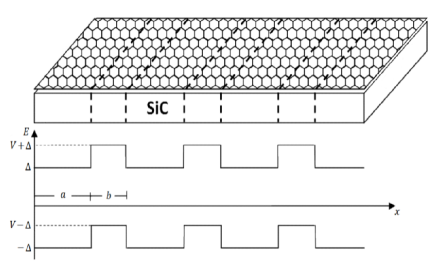
The electronic structure of a graphene sheet in the vicinity of a Dirac point K can be described by an effective Dirac Hamiltonian. Applying an external one-dimensional square-wave potential and considering an energy gap in the electronic structure of graphene, the Dirac-like Hamiltonian reads
| (1) |
where are the Pauli matrices, is the unitary matrix and is the Fermi velocity. The energy gap can be realized taking advantage of the influence of the substrate on the electronic properts of graphene. One can, for instance, deposit the graphene sheet in a SiC substrate Zhou et al. (2007), as shown in Fig. (1). Other important electronic property of graphene that is affected by the substrate is the Fermi velocity . For graphene in different substrates the Fermi velocity has been measured by different authors and their results summarized in Hwang et al. (2012). We are considering a periodic potential with period that is equal to at and zero at .
The Dirac equation is given by
| (2) |
where is a two-component spinor that represents the two graphene sublattices. Writing
| (3) |
and replacing in (2), one will have
| (4) |
Applying the unitary transformation , which commutes with and but not with on can write
| (5) | |||||
Using the property if we obtain that
| (6) |
Thus, we can define new effective mass and effective terms
| (7) |
Now, defining we make . So, the Hamiltonian (4) is reduced to
| (8) |
which is the two-dimensional massless Dirac equation for graphene with a periodic potential. The equation
| (9) |
was already solved by different methods Barbier, Vasilopoulos, and Peeters (2010); Arovas et al. (2010) and the dispersion relation is given by
| (10) | |||||
where , , is the Bloch wave number and we have defined . In order to transform back to the original and terms one can use the inverse transformation
| (11) |
As we define , we have that . Replacing this in Eq. (10) we obtain that the dispersion relation for a 2D massive Dirac equation with a periodic potential is given by
| (12) | |||||
where and . Note that at we recover the linear dispersion relation of a graphene sheet.
The left hand side of Eq. (12) is limited to the interval (-1,1). Therefore, in the right hand side one has allowed and forbidden values for the energy, which implies in the appearance of energy bands with gaps.
III The Electronic Structure
Having obtained the dispersion relation, in this section we will analyze the electronic structure. In what follows, we shall consider a constant period of the superlattice equal to nm, i.e., nm. As Eq. (12) is invariant under simultaneous replacements and , only non-negative values of will be considered. We shall concentrate our discussion on the valence and conductance minibands only, assuming the Fermi level to be in between at any value of V.
III.1 Band structure with equal well and barrier widths
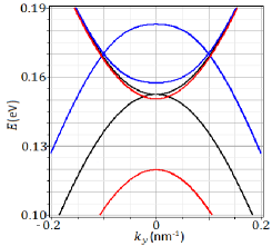
Here we will study the electronic band structure at nm in the dispersion relation (12), which means that the well and barrier have the same width. In Fig. 2 are plotted the electron and hole energies as a function of with and eV for meV (red), meV (black) and meV (blue). It can be seen that when the potential increases, the electron and hole minibands shift up. However, the shift of the electron miniband is not equal to the shift of the hole miniband, which implies different electron-hole minigaps for different values of , as shown in Fig. 2 . One can see that it is possible to close the minigap, as happens when meV (black), showing that is possible to have a gapped or gapless graphene only changing . It is a consequence of having a position dependent potential. If the potential is constant, the electron and hole minibands are shifted equally and the minigap remain the same, regardless of the value of the potential.

This is more clear when we look to Fig. 2 , where the electron and hole energies are plotted as a function of with . It should be noted that the contact point is obtained in , as can be seen in Fig. 2 . Therefore, Fig. 2 is showing how the electron-hole minigap changes with the potential for . It can be seen that the minigap oscillates when changes, and may be zero. For the values of the parameters chosen here, the first value of that closes the gap is meV. The highest value for the energy gap is obtained at , which is equal to . Thus, it is not possible to increase the initial gap in graphene with a periodic potential. It means that a periodic potential can tune the Dirac gap only in the range . So, if , the potential is not able to open a gap.
The electron and hole energies as a function of with are plotted in Fig. 3 for the same values of as in Fig. 2 . When meV (red) and meV (black) the minibands have the same behavior that in Fig. 2 , but are narrower. For meV (blue) the minigap at opens, however there are extra Dirac points appearing at different values of . These extra Dirac points appear when exceeds a critical value, that is for the values of the parameters chosen here, and do not disappear. So, from , the gapped graphene becomes gapless.
In order to find an expression for in terms of the system parameters, let us first localize the contact points in k space. Taking into account the implicit function theorem, one can conclude that at the contact points, where there is an intersection of the bands, the gradient (Jacobian) of the dispersion relation should be zero. Note that when and that the contact points are all at . So, the Eq. (12) with , and is given by
| (13) |
which is satisfied when , where is an integer different of zero, because implies , which makes the denominator in Eq. (13) vanishes. This condition leads to
| (14) |
which gives the values of where the contact points are located. The exact location of the contact points are . Should be remembered that the Dirac points appear only after a critical value of . The zeros of the equation above give the contact points at . So, one can write
| (15) |
which gives the values of where there is a contact point in Fig. 2 . The critical potential is given by .
The number of contact points can be found from Eq. (14). When is not an integer, the number of contact points is given by
| (16) |
where denotes an integer part. When , the number of Dirac points is . A different way to obtain the number of Dirac points is: when , , whereas when , .
III.2 Band structure with unequal well and barrier widths
Now let us consider the case with . The dashed lines in Fig. 4 are the minibands with nm and nm, whereas the continuum lines represent the minibands with nm and nm. In Fig. 4 are plotted the electron and hole minibands as a function of with at meV (red), meV (black) and meV (blue). As in the case with , for different values of there are different electron-hole minigaps, which may be zero. The oscillation of the minigap is shown in Fig. 4 , where the minibands as a function of with are plotted.

It can be seen that the values of that close the gap when and are the same for and . However, due to the fact that the potential shifts the minibands, when the graphene region with is wider than the region with , there is a larger shift of the minibands. It explains the difference in energy between the dashed and continuum lines in Fig. 4.
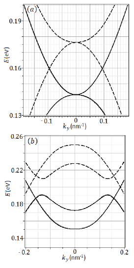
In Fig. 5 we plotted the minibands as a function of with . Once more, the dashed lines are the minibands with nm and nm, whereas the continuum lines are the minibands with nm and nm. In Fig. 5 we recovered the first time that the minigap closes at meV. In Fig. 5 we have meV. One can see that, when , the extra contact points that appears at are not in the Fermi level. When the contact points are shifted up (down) the Fermi level.
In order to localize the contact points, again, we take advantage of the implicit function theorem. The gradient of the dispersion relation will be zero only if and . So, one can write
| (17) |
and
| (18) |
where is an integer. Subtracting (18) from (17), one gets
| (19) |
Replacing the equation above in Eq. (17) one obtains
| (20) |
From the zeros of equation above one obtains,
| (21) |
which is the values of where there is a contact point in Fig. 4 . Again, the critical potential, where the graphene superlattice becomes gapless, is . One can see that increasing the difference between and the value of increases, as well. Therefore, for a particular , there is always a value of and which the graphene is gapped. When in Eqs. (19)-(21), the results obtained in the last section are recovered.

The exact location of the contact points when or is given by
| (22) |
where is the contact point nearest to , whereas is the contact point farthest to . Remember that in our system all contact points are at . An example is given in Fig. 6, where the electron and hole energies are plotted as a function of with nm, nm and meV. The location of the contact point nearest to is . The next nearest contact point is and the farthest contact point is located at .
The number of contact points is the same obtained in the last section with .
III.3 Dispersion relation near the contact points
Now, let us analyze the electronic structure near the contact points. The electronic structure in the vicinity of the contact points has been studied in the case of a gapless graphene superlattice Barbier, Vasilopoulos, and Peeters (2010) and for a graphene superlattice with spatially modulated gap Maksimova et al. (2012). In both cases, the discussion was restricted to the particular case . For the sake of comparison, we will consider the special case with and then consider the general case with . For this purpose, one has to expand Eq. (12) in the vicinity of the contact points obtained in the last sections.
Let us first consider the special case . In order to obtain the behavior of all contact points, one has to consider the contact points at , and and the contact points at , and . Thus, expanding Eq. (12) into the Taylor series up to second order of , and , one gets
| (23) | |||||
where we have defined , and . The positive and negative signs represent the electron and hole minibands, respectively. Writing and expanding Eq. (12) up to the lowest order of , and , one obtains the dispersion law in the vicinity of the contact points located at , which is given by
| (24) |
It should be noted that, when , the electron and hole minibands are symmetric related to , which does not happen when there is a periodic modulation of the energy gap in graphene Maksimova et al. (2012).
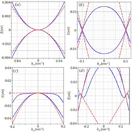
In Fig. 7 we plotted (dashed red line) with and as a function of and compare with the exact dispersion relation (12) (blue line). One can see that the expansion (23) is good in the vicinity of the contact point. Expanding in powers of with , one gets
| (25) |
which gives a parabolic electron and hole minibands, as can be seen in Fig. 7 , in contrast to the conical dispersion around the original Dirac point in a gapless graphene. In the limit when , the dispersion along becomes flat. Note that in the case of a gapless graphene superlattice Barbier, Vasilopoulos, and Peeters (2010), the dispersion along is given by . In Fig. 7 we compare (dashed red line) with Eq. (12) (blue line) at meV. Again, there is an agreement between the exact dispersion relation and the expansion (24) near the contact point. However, the dispersion is linear along , which does not happen in the contact points located at .
Considering now the most general case with , one can expand Eq. (12) with up to the lowest order of , and , and obtain the dispersion relation in the vicinity of the contact points at and , that is given by
| (26) |
The dispersion near the contact points at can be written as
| (27) |
where . The coefficients , and , with , depend on , , and . They are too large to be write down here. When , the coefficients and vanish and becomes . For this reason, it was necessary to expand Eq. (12) up to second order of , and to get .
One can note that, in contrast to the case with equal well and barrier widths, when the electron and hole minibands are not symmetric related to due to the coefficient . However, as in the case with , the minibands along the direction are parabolic in the contact points at and conical at . In Fig. 7 and we compare and , respectively, with the exact dispersion relation (12). We consider meV and plotted in the vicinity of the contact points located at .
Should be mentioned that the dispersion relation is linear along around all contact points. So, the energy surface is conical in the vicinity of the contact points at and has a lenslike shape around the contact points at .
III.4 Group velocity around the contact points
Let us now use the spectrum for small energies obtained above to find the effective Fermi velocity around the contact points. The components of the velocity in the vicinity of the contact points are given by and , where denote the four kinds of contact points. The expressions for the components of the velocity can be seen in the Appendix.
The anisotropy of the electron and hole velocities in the plane can be seen clearly if one introduces a polar angle with the relations and , where . In Fig. 8 the absolute value of the velocity as a function of was plotted for two different values of the energy gap: eV (continuum line) and meV (dashed line), which correspond to the graphene on a SiC and h-BN substrate, respectively. It should be mentioned that the Fermi velocity in graphene on these two substrate is m/s and m/s, respectively Hwang et al. (2012). One can see that the velocity is sensitive to the energy gap . The velocity has smaller values for larger values of .
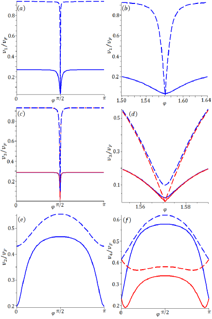
In Fig. 8 and we plotted the velocity for at ( meV when eV and meV when meV) and at the intermediate value between and ( meV when eV and meV when meV), respectively. When the electron and hole velocities are equal, in consequence of the symmetry between the electron and hole minibands. This does not happen in the case with a modulated energy gap Maksimova et al. (2012), where the electron and hole velocities are not the same. For small values of , is close to for almost all values of the angle , having a narrow dip in the vicinity of , as can be seen in Fig. 8 . This is due to the fact that is much greater than for all angle except in the vicinity of , where both and are small, in consequence of the lenslike shape of the energy surface. When increase the velocity decrease and the value of become much smaller than . The dip remains at , but it become a little wider. A similar behavior was obtained in Maksimova et al. (2012). In Fig. 8 there is a zoom of the dip region. Different of , the energy surface generated by is conical, but it is not an isotropic cone, generating an anisotropy in the velocity. In this case, with a small energy gap, the electron and hole velocities have only a little variation around , as can be seen in Fig. 8 . Increasing , there is a stronger anisotropy, in contrast with Maksimova et al. (2012).
The electron and hole velocities for nm and nm at ( meV when eV and meV when meV) and at the intermediate value between and ( meV when eV and meV when meV) are plotted respectively in Fig. 8 and . When the electrons and hole minibands are asymmetric, so the electron and hole velocities are not equal. In Fig. 8 we consider the contact point at . The behavior of the velocity in this case is very similar with the case with . The main difference is that the dip has a width slightly different. One can note that the electron and hole velocities are almost the same, differing slightly in the vicinity of . The Fig. 8 is an extension of the dip region. The energy surface generated by is conical, but is a tilted and not isotropic cone. In Fig. 8 we plotted . It can be seen that the electron and hole velocities are equal at and differ widely for other values of . As in the case with , when increases the anisotropy of the velocity becomes greater.
IV Conclusions
We have analyzed the electronic structure of a gapped graphene superlattice with a piecewise constant periodic potential using the continuum model based on an effective Dirac equation. We consider that the energy gap is generated by an appropriate substrate, which changes the Fermi velocity, as well.
It was shown that the energy gap oscillates when the potential changes continuously at and is zero at discrete values . When , extra Dirac points appear at and never disappear. Thus, beginning with a critical potential , the graphene system becomes gapless. In the special case of equal well and barrier widths, these extra Dirac points are located in the Fermi level and the electron and hole minibands are symmetric, whereas with an unequal well and barrier widths the extra Dirac points are no longer at the Fermi level and the electron and hole minibands are asymmetric. We found that if the initial energy gap in graphene is equal to , it is possible to tune the energy gap with a periodic potential in the range . We found the locations of all contact points and it was shown that the greater the difference between the well and barrier width, the greater the critical potential . Finally, we obtained the dispersion relation in the vicinity of all contact points and used it to find the effective group velocity of the carriers. The velocity has a strong anisotropy around the contact points and is sensitive to the energy gap. Extra Dirac points of different kinds have been already studied in graphene superlattices. Analyzing the electronic structure near the contact points, we showed that the extra Dirac points obtained here have a different behavior compared to previously studied. The results obtained here can be used in the fabrication of graphene–based devices.
Acknowledgements.
I thank M. A. H. Vozmediano for helping me to revise and correct mistakes in a previous version of the manuscript. This work was partially supported by CNPq and CNPq-MICINN binational.*
Appendix A The components of the group velocity around the contact points
The components of the velocity in the vicinity of the contact points are given by and , with . Thus,
| (28) |
| (29) |
| (30) |
| (31) |
| (32) |
| (33) |
| (34) |
and
| (35) |
where we define
| (36) |
| (37) |
| (38) |
and
| (39) |
References
- Novoselov et al. (2004) K. S. Novoselov, A. K. Geim, S. V. Morozov, D. Jiang, Y. Zhang, S. V. Dubonos, I. V. Grigorieva, and A. A. Firsov, Science 306, 666 (2004).
- Castro Neto et al. (2009) A. H. Castro Neto, F. Guinea, N. M. R. Peres, K. S. Novoselov, and A. K. Geim, Rev. Mod. Phys. 81, 109 (2009).
- Peres (2010) N. M. R. Peres, Rev. Mod. Phys. 82, 2673 (2010).
- Das Sarma et al. (2011) S. Das Sarma, S. Adam, E. H. Hwang, and E. Rossi, Rev. Mod. Phys. 83, 407 (2011).
- Katsnelson, Novoselov, and Geim (2006) M. I. Katsnelson, K. S. Novoselov, and A. K. Geim, Nat Phys 2, 620 (2006).
- Peres, Castro Neto, and Guinea (2006) N. M. R. Peres, A. H. Castro Neto, and F. Guinea, Phys. Rev. B 73, 241403 (2006).
- Gebhardt et al. (2013) J. Gebhardt, R. J. Koch, W. Zhao, O. Höfert, K. Gotterbarm, S. Mammadov, C. Papp, A. Görling, H.-P. Steinrück, and T. Seyller, Phys. Rev. B 87, 155437 (2013).
- Martins et al. (2007) T. B. Martins, R. H. Miwa, A. J. R. da Silva, and A. Fazzio, Phys. Rev. Lett. 98, 196803 (2007).
- Wang, Maiyalagan, and Wang (2012) H. Wang, T. Maiyalagan, and X. Wang, ACS Catalysis 2, 781 (2012).
- Giovannetti et al. (2007) G. Giovannetti, P. A. Khomyakov, G. Brocks, P. J. Kelly, and J. van den Brink, Phys. Rev. B 76, 073103 (2007).
- Ilyasov et al. (2014) V. V. Ilyasov, B. C. Meshi, V. C. Nguyen, I. V. Ershov, and D. C. Nguyen, The Journal of Chemical Physics 141, 014708 (2014).
- Zhou et al. (2007) S. Y. Zhou, G.-H. Gweon, A. V. Fedorov, P. N. First, W. A. de Heer, D.-H. Lee, F. Guinea, A. H. Castro Neto, and A. Lanzara, Nat Mater 6, 770 (2007).
- Hwang et al. (2012) C. Hwang, D. A. Siegel, S.-K. Mo, W. Regan, A. Ismach, Y. Zhang, A. Zettl, and A. Lanzara, Sci. Rep. 2, 590 (2012).
- Giavaras and Nori (2012) G. Giavaras and F. Nori, Phys. Rev. B 85, 165446 (2012).
- De Martino, Dell’Anna, and Egger (2007) A. De Martino, L. Dell’Anna, and R. Egger, Phys. Rev. Lett. 98, 066802 (2007).
- Giavaras, Maksym, and Roy (2009) G. Giavaras, P. A. Maksym, and M. Roy, Journal of Physics: Condensed Matter 21, 102201 (2009).
- Maksym et al. (2010) P. A. Maksym, M. Roy, M. F. Craciun, S. Russo, M. Yamamoto, S. Tarucha, and H. Aoki, Journal of Physics: Conference Series 245, 012030 (2010).
- Peres (2009) N. M. R. Peres, Journal of Physics: Condensed Matter 21, 095501 (2009).
- Giavaras and Nori (2010) G. Giavaras and F. Nori, Applied Physics Letters 97, 243106 (2010).
- Lima and Moraes (2015) J. R. F. Lima and F. Moraes, Solid State Communications 201, 82 (2015).
- Lima (2015) J. R. F. Lima, Physics Letters A 379, 179 (2015).
- Bai and Zhang (2007) C. Bai and X. Zhang, Phys. Rev. B 76, 075430 (2007).
- Barbier et al. (2008) M. Barbier, F. M. Peeters, P. Vasilopoulos, and J. M. Pereira, Phys. Rev. B 77, 115446 (2008).
- Park et al. (2008a) C.-H. Park, L. Yang, Y.-W. Son, M. L. Cohen, and S. G. Louie, Phys. Rev. Lett. 101, 126804 (2008a).
- Barbier, Vasilopoulos, and Peeters (2009) M. Barbier, P. Vasilopoulos, and F. M. Peeters, Phys. Rev. B 80, 205415 (2009).
- Tiwari and Stroud (2009) R. P. Tiwari and D. Stroud, Phys. Rev. B 79, 205435 (2009).
- Wang and Zhu (2010) L.-G. Wang and S.-Y. Zhu, Phys. Rev. B 81, 205444 (2010).
- Barbier, Vasilopoulos, and Peeters (2010) M. Barbier, P. Vasilopoulos, and F. M. Peeters, Phys. Rev. B 81, 075438 (2010).
- Wang and Chen (2011) L.-G. Wang and X. Chen, Journal of Applied Physics 109, 033710 (2011).
- Maksimova et al. (2012) G. M. Maksimova, E. S. Azarova, A. V. Telezhnikov, and V. A. Burdov, Phys. Rev. B 86, 205422 (2012).
- Ramezani Masir et al. (2008) M. Ramezani Masir, P. Vasilopoulos, A. Matulis, and F. M. Peeters, Phys. Rev. B 77, 235443 (2008).
- Ghosh and Sharma (2009) S. Ghosh and M. Sharma, Journal of Physics: Condensed Matter 21, 292204 (2009).
- Ramezani Masir, Vasilopoulos, and Peeters (2009) M. Ramezani Masir, P. Vasilopoulos, and F. M. Peeters, Phys. Rev. B 79, 035409 (2009).
- Dell’Anna and De Martino (2009) L. Dell’Anna and A. De Martino, Phys. Rev. B 79, 045420 (2009).
- Zhai and Chang (2012) F. Zhai and K. Chang, Phys. Rev. B 85, 155415 (2012).
- Moldovan et al. (2012) D. Moldovan, M. Ramezani Masir, L. Covaci, and F. M. Peeters, Phys. Rev. B 86, 115431 (2012).
- Marchini, Günther, and Wintterlin (2007) S. Marchini, S. Günther, and J. Wintterlin, Phys. Rev. B 76, 075429 (2007).
- Vázquez de Parga et al. (2008) A. L. Vázquez de Parga, F. Calleja, B. Borca, M. C. G. Passeggi, J. J. Hinarejos, F. Guinea, and R. Miranda, Phys. Rev. Lett. 100, 056807 (2008).
- Sutter, Flege, and Sutter (2008) P. W. Sutter, J.-I. Flege, and E. A. Sutter, Nat Mater 7, 406 (2008).
- Martoccia et al. (2008) D. Martoccia, P. R. Willmott, T. Brugger, M. Björck, S. Günther, C. M. Schlepütz, A. Cervellino, S. A. Pauli, B. D. Patterson, S. Marchini, J. Wintterlin, W. Moritz, and T. Greber, Phys. Rev. Lett. 101, 126102 (2008).
- Rusponi et al. (2010) S. Rusponi, M. Papagno, P. Moras, S. Vlaic, M. Etzkorn, P. M. Sheverdyaeva, D. Pacilé, H. Brune, and C. Carbone, Phys. Rev. Lett. 105, 246803 (2010).
- Yan et al. (2013) H. Yan, Z.-D. Chu, W. Yan, M. Liu, L. Meng, M. Yang, Y. Fan, J. Wang, R.-F. Dou, Y. Zhang, Z. Liu, J.-C. Nie, and L. He, Phys. Rev. B 87, 075405 (2013).
- Brey and Fertig (2009) L. Brey and H. A. Fertig, Phys. Rev. Lett. 103, 046809 (2009).
- Park et al. (2009) C.-H. Park, Y.-W. Son, L. Yang, M. L. Cohen, and S. G. Louie, Phys. Rev. Lett. 103, 046808 (2009).
- Park et al. (2008b) C.-H. Park, Y.-W. Son, L. Yang, M. L. Cohen, and S. G. Louie, Nano Letters 8, 2920 (2008b).
- Bliokh et al. (2009) Y. P. Bliokh, V. Freilikher, S. Savel’ev, and F. Nori, Phys. Rev. B 79, 075123 (2009).
- Uddin and Chan (2014) S. Uddin and K. S. Chan, Journal of Applied Physics 116, 203704 (2014).
- Arovas et al. (2010) D. P. Arovas, L. Brey, H. A. Fertig, E.-A. Kim, and K. Ziegler, New Journal of Physics 12, 123020 (2010).