Shot noise of the edge transport in the inverted band HgTe quantum wells.
Abstract
We investigate the current noise in HgTe-based quantum wells with an inverted band structure in the regime of disordered edge transport. Consistent with previous experiments, the edge resistance strongly exceeds and weakly depends on the temperature. The shot noise is well below the Poissonian value and characterized by the Fano factor with gate voltage and sample to sample variations in the range . Given the fact that our devices are shorter than the most pessimistic estimate of the ballistic dephasing length, these observations exclude the possibility of one-dimensional helical edge transport. Instead, we suggest that a disordered multi-mode conduction is responsible for the edge transport in our experiment.
The topological insulator (TI) concept 1 allows to predict whether a general band insulator contains gap-less electronic surface states based solely on the symmetry considerations. If present, such states possess a linear dispersion relation along with a topological protection from elastic backscattering 2. Though such Weyl-type states in semiconductor inverted band interfaces have been known since about three decades 3, their topological origin was hidden until recently. Surface states of a two-dimensional (2D) TI are represented by one-dimensional (1D) helical edge states, protected from elastic backscattering and propagating along the boundary between the 2D TI and the normal insulator or vacuum.
The 2D TI phase has been proposed in HgTe 4 and InAs/GaSb 5 quantum wells with the inverted band structure. Experimental evidence of the edge transport near the charge neutrality point (CNP) in such structures comes from a nearly quantized resistance in short samples 6; 7, strongly nonlocal transport 8; 9; 10, current density visualization 11 and Josephson interference experiments 12. More recently, the edge states contribution was identified in conductance of the lateral p-n junctions in HgTe 13. In samples longer than a few micrometers the regime of disordered edge transport is realized. Here the resistance scales with the device length 6; 14; 10 whereas its temperature () dependence is very weak 9; 10. These observations is hard to reconcile with the theoretical models that consider inelastic scattering to account for the dephasing and broken topological protection, see e.g. Refs. 15; 16.
At a given the dephasing time is fundamentally bounded from below by the uncertainty principle , where and are the Planck constant and the Boltzman constant, regardless the actual dephasing mechanism 17. At K, with the helical edge state velocity of m/s 18, this corresponds to the ballistic dephasing length of m in HgTe quantum wells. Along with the weak dependence, this suggests that in a few micrometer long HgTe devices the transport may already be coherent. This conjecture can be directly tested via the measurement of the current fluctuations (shot noise), that is related 19 to the quantum-mechanical transmission probability via the Fano factor , where and are, respectively the sample resistance and the resistance quantum.
In this Letter, we investigate the current noise in the regime of disordered edge transport () near the CNP in the inverted band HgTe quantum wells. At low the devices are well in the regime , where is the length of the edge state. The shot noise Fano factor exhibits gate voltage and sample to sample variations in the range . At the same time, the dependence of the resistance is weakly insulating. These observations preclude the possibility of 1D helical edge states and suggest a multi-mode diffusive conduction as the origin of the edge transport in our devices. Our data clearly demonstrates that a presumption of the single-channel helical edge transport in the inverted band structures calls for an independent verification.
Our samples are based on 8 nm wide (013) CdHgTe/HgTe/CdHgTe quantum wells grown by molecular beam epitaxy, with mesas shaped by wet etching and covered with a insulating layer, see Ref. 22 for the details. Metallic Au/Ti top gates enable us to tune the 2D system across the CNP by means of a field effect. Ohmic contacts are achieved by a few second In soldering in air, providing a typical resistance of the ungated mesa arms in the range of 10-30 at low . The experiment was performed in a liquid 3He insert with a bath of 0.52 K. The dc transport measurements were performed in a two-terminal or multi-terminal configurations with the help of a low-noise 100 M input resistance preamplifier. The shot noise voltage fluctuation is measured within a frequency band 10-20 MHz by means of a 10 load resistor, a 15 MHz resonant tank circuit and a home-made 10 dB cryogenic rf-amplifier followed by a dB room- amplification stage and a power detector. The noise measurement setup was calibrated via the Johnson-Nyquist thermometry. Below we present the results obtained on three samples which demonstrate similar behavior reproducible in respect to thermal recycling. The sample I had a mobility of about at an electron density of measured at a zero gate voltage. The sample II was not characterized and is expected to have a similar quality. The lower quality sample III had a mobility of about at an electron density of about measured in the ungated region.
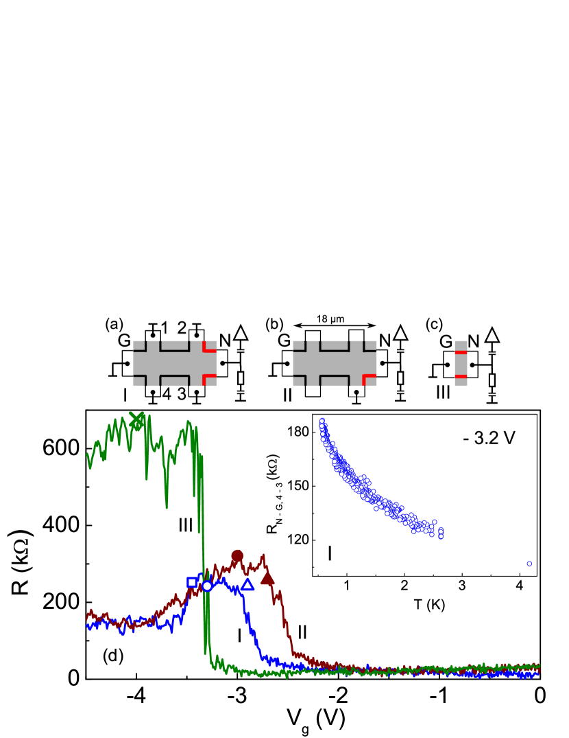
In figs. 1a, 1b and 1c we sketch the experimental layouts used for two-terminal transport and noise measurements, respectively, in samples I, II and III. All the dimensions correspond to those in real samples, see the scale bar. The top gated areas are shaded in grey and the edges of the gated part of the mesa are shown by thick solid lines. The bonded and floating ohmic contacts are marked, respectively, by the dotted and open rectangles. In all cases, the contact was connected to the circuit ground and the contact was used for both dc transport and rf noise measurements. This was achieved by means of the load resistor capacitively coupled to the ground, and a 10 nF capacitor coupled to the input of the cryogenic rf-amplifier (depicted by a triangle). All other bonded contacts were capacitively coupled to the ground at low and could be grounded, connected to the dc circuit at a room or left floating. The edge states mainly contributing to the noise signal in the edge transport regime are marked by the thicker lines. Their nominal lithographic length is about 4 m in samples I and II and 3 m in sample III.
In fig. 1d we plot the gate voltage () dependencies of the two terminal linear response resistance () measured in configurations of figs. 1a, 1b and 1c at K. At not too negative the contribution of the ohmic contacts and respective mesa arms dominates . In samples I and II, at decreasing the 2D system is tuned 9 from the -type to the -type conduction across the CNP at V, where exhibits a pronounced peak. At more negative the resistance somewhat decreases and saturates in the -type region. In sample III we observe only a steep rise of followed by a plateau which continues up to the lowest achievable V. Thus, in this sample, the location of the CNP is uncertain and below we assume that it belongs somewhere in the middle of the plateau (marked by a cross). The inset of fig. 1d demonstrates the dependence of the four terminal resistance in sample I at V with source , drain and potential contacts 3 and 4. The dependence is weakly insulating, such that the resistance increases by less than a factor of 2 when the is lowered between 4.2 K and 0.5 K. Other samples behave similarly in the CNP region. Note that the transport data of fig. 1d is consistent with previous measurements on similar samples, including reproducible mesoscopic-like resistance fluctuations 23.

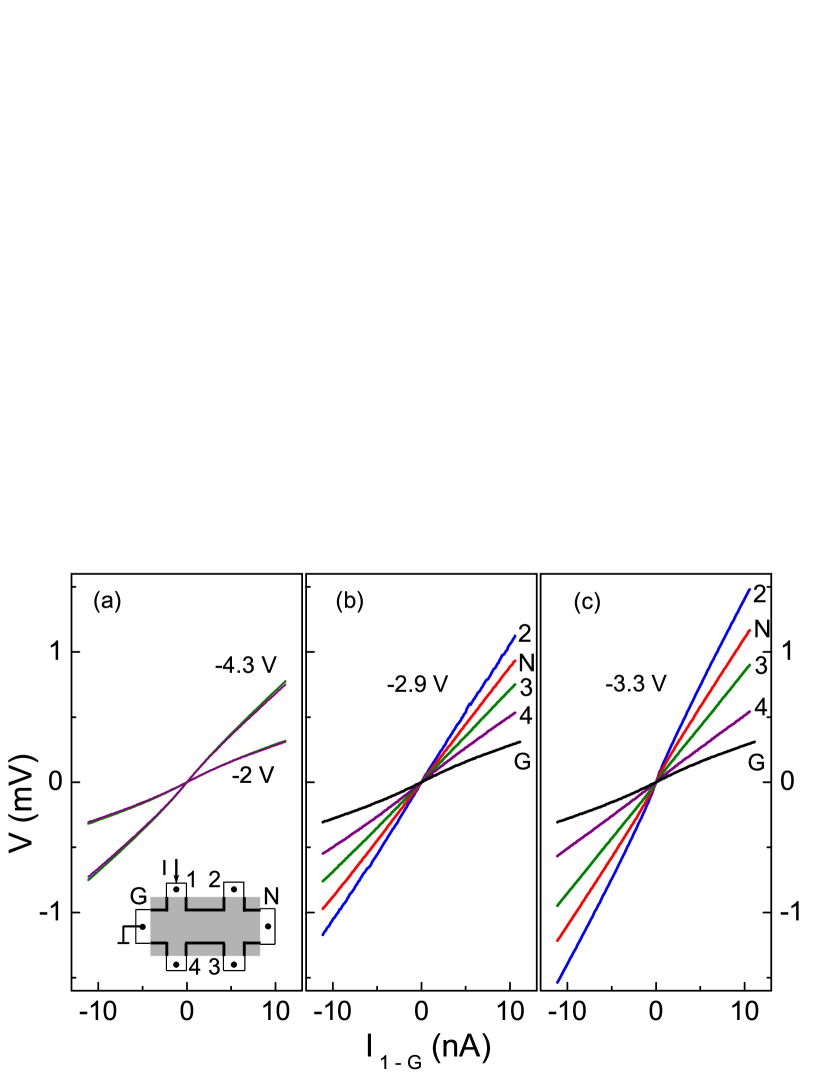
Fig. 2 demonstrates that near the CNP the transport current in our samples flows around the mesa edges under the gate. In this figure we plot the set of three terminal - curves measured in sample I. Here, the source contact is 1, the ground contact is and the voltage on the contact probes 2, , 3 and 4 is measured in respect to the ground potential (see the inset of fig. 2a for contacts labels). The data of fig. 2a demonstrates a bulk transport under the gate outside the region near the CNP. At the highest V, the sample is well in the regime of -type conduction and the - curves are almost indistinguishable. In this case the voltage drop below the gate is negligible and we measure simply the - curve of the contact G and its mesa arms. Similar situation is the case for the lowest V, where the sample is well in the -type conduction regime. In contrast, as shown in figs. 2b and 2c, at V and V the - curves measured with the four different contacts vary considerably. In these cases, the dependence of on the contact number corresponds to their clockwise order ( is the highest for the contact 2 and the lowest for the contact 4), as expected for the edge transport 9. We have checked that around the CNP the transport remains strongly non-local at least up to meV and K without significant bulk contribution. This ensures that the noise measurements presented below are performed strictly in the regime of edge transport. Note that the edge resistances deduced from fig. 2 do not scale properly with the length of the edge segments, that we attribute to the sample inhomogeneity.

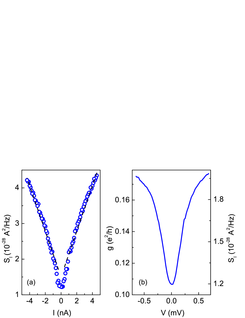
In fig. 3a we plot the dependence of the noise spectral density on in the CNP region in sample I, measured in the configuration of fig. 1a. At increasing the noise increases above the equilibrium Johnson-Nyquist value and crosses over to a slightly sublinear dependence on . Such a dependence permits only a rough estimate of the shot noise Fano factor (the dashed guide line in Fig. 3a has a slope of ). We find that the nonlinearity of vs is a result of the interplay of Johnson-Nyquist noise and nonlinear transport regime. Fig. 3b demonstrates the bias dependence of the differential conductance obtained by a numerical differentiation of the - curve. At increasing we observe a rapid increase of roughly by about a factor of 1.5 which tends to level off at higher bias voltages. A corresponding variation of the Johnson-Nyquist noise, estimated as , would account for about 20% of the noise increase in fig. 3a.
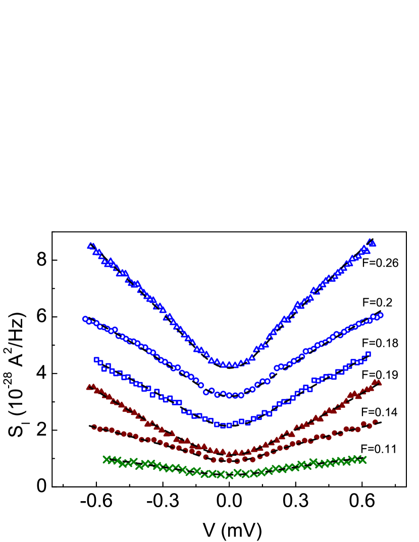
For a more accurate analysis, below we use an approximate expression for the shot noise in the nonlinear transport regime, analogous to the noise studies in ballistic quantum point contacts 24 and graphene transistors 25: , where and is a direct analogue of the Fano factor in the nonlinear transport regime. As shown in fig. 4, this expression provides a nearly perfect fit 26 (dashed line) for the experimental dependence (open circles) and allows to quantify the Fano factor as .

In fig. 4 we plot the results of the noise measurements (symbols) at different in the CNP region in samples I, II and III. For each sample the gate voltage positions are marked by the same symbols in fig. 1d . Each dataset in fig. 4 is accompanied by a fit (dashed lines) along with the value of and some are vertically offset for clarity (see caption). Similar to fig. 3b, we find that the above expression for i s very well consistent with the experiment up to the bias voltages of about 0.6 mV, corresponding to . In all measurements we observe a finite shot noise suppressed well below the Poissonian value () with gate voltage and sample to sample variations of the Fano factor in the range . These variations appear random, not correlated with the variations of the conductance, the lithographic length of the gated mesa edges or the experimental geometry (see fig. 1).

Obviously, our observations exclude coherent 1D transport scenario, which would result in a nearly Poissonian noise () given the edge resistance large compared to the resistance quantum . On the other hand, at K the ballistic dephasing length of the helical edge states m is at least comparable to the device length m and by far exceeds the localization length estimated as nm. In single-channel 1D transport the condition is equivalent to strong carrier localization, that is in contrast with the dependence of the resistance in our devices, see the inset of fig. 1d. Based on previous experiments 9; 14 we find that exotic scenarios like a couple of strong scatterers per edge state or a large spreading resistance in the ungated area 27 are unlikely in present samples. Hence, the above discrepancies manifest the breakdown of the concept of 1D helical edge transport in our devices.
Instead, the experiment is qualitatively compatible with a disordered multi-mode quasi-1D transport along the edge, that might result from a smooth edge profile (see, e.g., Ref. 3) or a trivial electrostatic band bending on the edge. In this case, the strong localization does not occur for smaller than the time of diffusion on the length scale of , that is , where is the number of transverse modes and is the Fermi velocity. This condition is much less strict compared to the case of 1D helical edge (). Regarding the noise data, the moderate reduction of the Fano factor below , the universal value for diffusive conduction, in our experiment can result from the energy relaxation to the external bath 20; 21; 19. In principle, the energy relaxation can be sensitive to both the edge structure and the carrier density that might explain the observed variations of .
In summary, we investigated the shot noise of the disordered edge transport in the inverted band HgTe quantum wells. The length of the devices is short compared to the dephasing length and the edge resistance is large compared to . The shot noise Fano factor exhibits gate voltage and sample to sample variations in the range , whereas the dependence of the resistance is weakly insulating. These observations are in stark contrast with the scenario of 1D helical edge transport. We suggest, that the disordered multi-mode quasi-1D transport is involved, that might result from the smooth edge profile or the band bending. While the fate of the helical edge states and their topological protection remains unclear, we find that a presumption of the single-channel edge transport in the inverted band structures calls for an independent verification.
We gratefully acknowledge discussions with I.S. Burmistrov, V.T. Dolgopolov and K.E. Nagaev. A financial support from the Russian Academy of Sciences, RFBR Grants No. 15-02-04285a and No. 13-02-12127ofi, the Ministry of Education and Science of the Russian Federation Grants No. 14Y.26.31.0007 and 14.587.21.0006 (RFMEFI58714X0006) is acknowledged.
References
- (1) M.Z. Hasan and C.L. Kane, Rev. Mod. Phys. 82, 3045 (2010); X.-L. Qi and S.-C. Zhang, ibid. 83, 1057 (2011).
- (2) C.L. Kane, E.J. Mele, Phys. Rev. Lett. 95, 146802 (2005).
- (3) B.A. Volkov and O.A. Pankratov, Pis’ma Zh. Eksp. Teor. Fiz. 42, 145 (1985) [JETP Lett. 42, 178 (1985)].
- (4) B.A. Bernevig, T.L. Hughes, S.-C. Zhang, Science 314, 1757 (2006).
- (5) C. Liu, T.L. Hughes, X.-L. Qi, K. Wang, and S.-C. Zhang, Phys. Rev. Lett. 100, 236601 (2008).
- (6) M. Koenig, S. Wiedmann, C. Bruene, A. Roth, H. Buhmann, L.W. Molenkamp, X.-L. Qi, and S.-C. Zhang, Science 318, 766 (2007).
- (7) I. Knez, R.-R. Du, and G. Sullivan, Phys. Rev. Lett. 107, 136603 (2011).
- (8) A. Roth, C. Bruene, H. Buhmann, L.W. Molenkamp, J. Maciejko et al., Science 325, 294 (2009).
- (9) G.M. Gusev, Z.D. Kvon, O.A. Shegai, N.N. Mikhailov, S.A. Dvoretsky, and J.C. Portal, Phys. Rev. B 84, 121302(R) (2011).
- (10) I. Knez, C.T. Rettner, S.-H. Yang, S.S. P. Parkin, L. Du, R.-R. Du, G. Sullivan, Phys. Rev. Lett. 112, 026602 (2014).
- (11) K.C. Nowack, E.M. Spanton, M. Baenninger, M. Koenig, J.R. Kirtley et al., Nature Mat. 12, 787 (2013).
- (12) S. Hart, H. Ren, T. Wagner, P. Leubner, M. Muehlbauer, C. Brueune et al., Nature Physics 10, 638–643 (2014).
- (13) G.M. Minkov, A.A. Sherstobitov, A.V. Germanenko, O.E. Rut, S.A. Dvoretsky, N.N. Mikhailov, Pis’ma v ZhETF 101, 522 (2015).
- (14) G.M. Gusev, Z.D. Kvon, E.B. Olshanetsky, A.D. Levin, Y. Krupko, J.C. Portal, N.N. Mikhailov, and S.A. Dvoretsky, Phys. Rev. B 89, 125305 (2014).
- (15) J.I. Vaeyrynen, M. Goldstein, and L. I. Glazman, Phys. Rev. Lett. 110, 216402 (2013).
- (16) N. Kainaris, I.V. Gornyi, S.T. Carr, A.D. Mirlin, Phys. Rev. B 90, 075118 (2014).
- (17) B.L. Altshuler, A.G. Aronov, in: A.L. Efros, M. Pollak (Eds.), Electron-electron Interactions in Disordered Conductors, Elsevier Science Publishers B.V. (1985).
- (18) O.E. Raichev, Phys. Rev. B 85, 045310 (2012).
- (19) Ya. M. Blanter and M. Buttiker, Phys. Rep. 336, 1 (2000).
- (20) K.E. Nagaev, Phys. Lett. A 169, 103 (1992).
- (21) M.J.M. de Jong, C.W.J. Beenakker, Physica A 230, 219 (1996).
- (22) E.B. Olshanetsky, Z.D. Kvon, M.V. Entin, L.I. Magarill et al., Pis’ma Zh. Eksp. Teor. Fiz. 89, 338 (2009) [JETP Lett. 89, 290 (2009)].
- (23) G. Grabecki, J. Wrobel, M. Czapkiewicz, Ł. Cywinski, S. Gierałtowska et al., Phys. Rev. B 88, 165309 (2013).
- (24) P. Roche, J. Segala, D.C. Glattli, J.T. Nicholls, M. Pepper, A.C. Graham, K.J. Thomas, M.Y. Simmons, and D.A. Ritchie, Phys. Rev. Lett. 93, 116602 (2004); L. DiCarlo, Y. Zhang, D.T. McClure, D.J. Reilly, C.M. Marcus, L.N. Pfeiffer, and K.W. West, Phys. Rev. Lett. 97, 036810 (2006); S. Nakamura, M. Hashisaka, Y. Yamauchi, S. Kasai, T. Ono, and K. Kobayashi, Phys. Rev. B 79, 201308 (2009).
- (25) L. DiCarlo, J.R. Williams, Y. Zhang, D.T. McClure, and C.M. Marcus, Phys. Rev. Lett. 100, 156801 (2008).
- (26) The fit quality worsens if the nonlinear conductance is used instead of in the expression for .
- (27) A. Kononov, S.V. Egorov, Z.D. Kvon, N.N. Mikhailov, S.A. Dvoretsky, E.V. Deviatov, arXiv:1410.0585 (2014).