Raman Spectroscopy of Electrochemically-Gated Graphene Transistors: Geometrical Capacitance, Electron-Phonon, Electron-Electron, and Electron-Defect Scattering
Abstract
We report a comprehensive micro-Raman scattering study of electrochemically-gated graphene field-effect transistors. The geometrical capacitance of the electrochemical top-gates is accurately determined from dual-gated Raman measurements, allowing a quantitative analysis of the frequency, linewidth and integrated intensity of the main Raman features of graphene. The anomalous behavior observed for the G-mode phonon is in very good agreement with theoretical predictions and provides a measurement of the electron-phonon coupling constant for zone-center ( point) optical phonons. In addition, the decrease of the integrated intensity of the 2D-mode feature with increasing doping, makes it possible to determine the electron-phonon coupling constant for near zone-edge (K and K’ points) optical phonons. We find that the electron-phonon coupling strength at is five times weaker than at K (K’), in very good agreement with a direct measurement of the ratio of the integrated intensities of the resonant intra- (2D’) and inter-valley (2D) Raman features. We also show that electrochemical reactions, occurring at large gate biases, can be harnessed to efficiently create defects in graphene, with concentrations up to approximately . At such defect concentrations, we estimate that the electron-defect scattering rate remains much smaller than the electron-phonon scattering rate. The evolution of the G- and 2D-mode features upon doping remain unaffected by the presence of defects and the doping dependence of the D mode closely follows that of its two-phonon (2D mode) overtone. Finally, the linewidth and frequency of the G-mode phonon as well as the frequencies of the G- and 2D-mode phonons in doped graphene follow sample-independent correlations that can be utilized for accurate estimations of the charge carrier density.
pacs:
78.67.Wj, 78.30.-j, 72.80.Vp, 63.22.Rc, 63.20.kd, 82.45.-hI Introduction
Graphene, as an atomically thin two-dimensional crystal, features an electron gas that is directly exposed to its local environment. As a result, graphene is uniquely sensitive to external stimuli. This is remarkably illustrated by the electric field effect, which makes it possible to swiftly tune the carrier density of graphene (i.e., its Fermi energy ) and, in return, to control a wealth of fundamental properties, among which, the electrical Novoselov et al. (2004); Zhang et al. (2005); Novoselov et al. (2005) and optical conductivities,Wang et al. (2008); Li et al. (2008); Mak et al. (2014) as well as of the electron-phonon coupling.Yan et al. (2007); Pisana et al. (2007) From a more applied standpoint, the unique controllability of graphene can be harnessed in a variety of nano-devices.Novoselov et al. (2012)
Among the various experimental techniques employed to study graphene, Raman scattering spectroscopy Malard et al. (2009); Ferrari and Basko (2013) stands out as a fast, sensitive, and minimally invasive tool in order to probe electron-phonon,Yan et al. (2007); Pisana et al. (2007); Berciaud et al. (2010); Chae et al. (2010); Freitag et al. (2010) electron-electron Basko et al. (2009) and electron-defect scattering Bruna et al. (2014); Liu et al. (2013) at variable carrier density. Raman spectroscopy is also routinely employed to characterize unintentional doping in graphene Casiraghi et al. (2007); Berciaud et al. (2009); Ni et al. (2009) and to study the sensitivity of graphene to atmospheric Ryu et al. (2010) and chemical dopants.Jung et al. (2009); Zhao et al. (2010); Jung et al. (2011); Howard et al. (2011); Crowther et al. (2012); Parret et al. (2013); Chen et al. (2014) Quantitative investigations of doped graphene are particularly relevant, since several interesting phenomena, such as superconductivity,McChesney et al. (2010); Profeta et al. (2012); Nandkishore et al. (2012) ferromagnetism,Ma et al. (2010) charge or spin density waves,Li et al. (2010); Makogon et al. (2011) as well as changes in the plasmon spectrum Koppens et al. (2011); García de Abajo (2014) are expected to occur in the strong doping regime .
In practice, solid state graphene field-effect transistors (FETs), typically using a Si substrate as a back-gate and a SiO2 epilayer as a gate dielectric, have been widely used to study the Raman response of graphene in the vicinity of the Dirac point .Yan et al. (2007); Pisana et al. (2007); Yan et al. (2008); Araujo et al. (2012) To access higher doping levels, other methodologies based on chemical doping Jung et al. (2009); Zhao et al. (2010); Jung et al. (2011); Howard et al. (2011); Crowther et al. (2012); Parret et al. (2013); Chen et al. (2014) and electrochemical gating Lu et al. (2004); Kim et al. (2013); Das et al. (2008) have been introduced. The former is highly efficient, resulting in charge carrier concentrations exceeding , but is irreversible and little controllable. The latter, which relies on the formation of nanometer-thin electrical double layers (EDL) with high geometrical capacitance, makes it possible to reversibly attain electron or hole concentrations as high as , at cryogenic temperatures.Efetov and Kim (2010) Recently, electrochemically-gated graphene FETs have been successfully employed to investigate electron-phonon coupling,Das et al. (2008); Yan et al. (2009); Das et al. (2009); Kalbac et al. (2010); Chen et al. (2011); Chattrakun et al. (2013) but also bandgap formation in bilayer graphene,Mak et al. (2009); Zhang et al. (2009) electron transport at high carrier density,Efetov and Kim (2010); Efetov et al. (2011); Ye et al. (2011) many-body phenomena,Mak et al. (2014) as well as to electrically control the interaction between nano-emitters and graphene.Lee et al. (2014); Tielrooij et al.
In such studies, an accurate determination of (hence of the gate capacitance) as a function of the gate voltage is a critical requirement. However, as opposed to solid state FETs, in which the oxide dielectric constant and thickness can be known with accuracy, the thickness of the electrical double layer may be highly sensitive to the device geometry, fluctuate spatially and vary over time. This further highlights the need for (i) robust methods for device fabrication and, (ii) accurate tools to experimentally measure the gate capacitance. In previous works, the gate capacitance of electrochemically gated graphene FETs has been evaluated from an estimation of the thickness of the EDL,Das et al. (2008, 2009) from capacitance Xia et al. (2009); Uesugi et al. (2013) or Hall measurements,Ye et al. (2011); Efetov and Kim (2010); Efetov et al. (2011); Bruna et al. (2014) or from optical absorption spectroscopy. Chen et al. (2011); Mak et al. (2014)
In this article, we show that micro-Raman scattering measurements on electrochemically top-gated and SiO2 back-gated graphene FETs can be used to accurately determine the geometrical capacitance of the electrical double layer and hence , with a spatial resolution down to approximately . Calibrated electrochemical gates allow us (i) to quantitatively compare the anomalous doping-dependence of the G-mode phonon to theoretical models,Ando (2006); Lazzeri and Mauri (2006); Pisana et al. (2007) (ii) to deduce the electron-phonon coupling constants at the center ( point) and near the edges ( and points) of the Brillouin zone of graphene,Basko et al. (2009) and (iii) to establish well-defined correlations between the frequencies, linewidths and integrated intensities of the main Raman features in doped graphene. Importantly, we show that at top-gate voltages beyond the threshold for electrochemical reactions, defect concentrations of up to approximately can be created without damaging the device. This allows us, in particular, to quantitatively investigate the doping dependence of the defect-related D mode and to estimate the electron-defect scattering rate in graphene.
The paper is organized as follows: the experimental methods are exposed in Sec. II. Section III presents a model for the electric field effect in electrochemically-gated graphene FETs. Section IV is dedicated to the experimental determination of the geometrical capacitance of the electrical double layer. In Sec. V we specifically address electron-phonon coupling in pristine graphene. Section VI describes our study of defective graphene and the determination of the electron-defect scattering rate. Finally, in Sec. VII, we describe the correlations between the main Raman features in doped graphene.
II Methods
II.1 Sample preparation
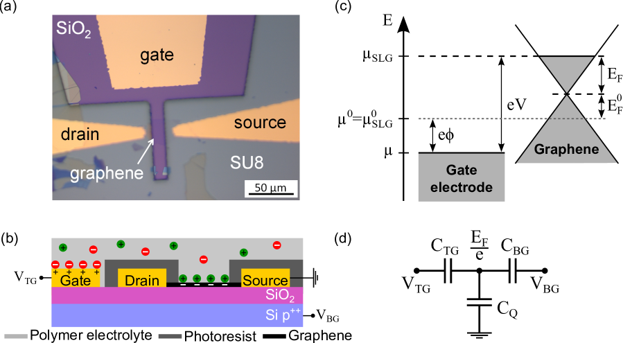
Graphene samples are produced by mechanical exfoliation of natural graphite onto highly -doped Si substrates covered with a ( SiO2 epilayer. Graphene monolayers are identified by optical microscopy and micro-Raman spectroscopy. Source, drain and gate electrodes are made by photolithography, followed by metal deposition (Ti (3 nm)/Au (47 nm)). The device are then coated with a 4 m thick photoresist layer (MicroChem SU8 2005), and a second photolithography step is performed to open a window above the graphene channel and gate electrode, as shown in Fig. 1(a)-(b). Finally, the electrochemical top-gate is formed by depositing a drop of polymer electrolyte with a micropipette. The polymer electrolyte is prepared by mixing lithium perchlorate (LiClO4) and polyethylene oxide (PEO) in methanol at a weight ratioDas et al. (2008); Lu et al. (2004); Liu et al. (2013) 0.012:1:4. The mixture is then heated at 45 ∘C and stirred until it becomes uniform. This suspension is filtered to get a clear solution. After dropcasting, the methanol evaporates and a thin film of transparent polymer electrolyte is formed. To remove residual moisture and solvent, the devices are annealed at about 90 . Noteworthy, the device geometry depicted in Fig. 1(a)-(b) features a well-defined gated region and prevents the polymer electrolyte to be in contact with the source and drain electrodes. As compared to earlier works, Das et al. (2008, 2009); Yan et al. (2009) this improves the gating efficiency and reduces the electrochemical reactivity of our devices. Some measurements described in the following are performed in a dual-gated geometry. In this case, the back-gate voltage is applied using the Si substrate as a gate electrode.
II.2 Experimental setup
We perform micro-Raman scattering measurements in ambient conditions on top-gated and dual-gated graphene field-effect transistors. Raman spectra are recorded in a backscattering geometry, with a home-built setup, using a 40 objective (NA = 0.60) and a 532 nm laser beam focused onto a spot of approximately in diameter. The sample holder is mounted onto a x-y-z piezoelectric stage, allowing spatially resolved Raman studies. The collected Raman scattered light is dispersed onto a charged-coupled device (CCD) array by a single-grating monochromator, with a spectral resolution of about . The laser beam is linearly polarized and the laser power is maintained below 500 , in order to avoid thermally induced spectral shifts or lineshape modifications of the Raman features,Calizo et al. (2007) as well as photo-electrochemical reactions.Kalbac et al. (2010); Efetov and Kim (2010); Bruna et al. (2014) The sample holder is electrically connected to a sourcemeter, which triggers our CCD array. Raman spectra are recorded as a function of the applied gate bias, once a steady gate leak current (typically lower than 100 pA in the electrochemically top-gated configuration) is achieved. For this purpose, the gate bias is first applied for a settling time of 1 min, before recording each Raman spectrum. This procedure ensures that Raman spectra are recorded at constant charge carrier densities. Raman spectra are also recorded during several forward and backward top-gate sweeps at the same spot on a given sample and very reproducible results, with no significant hysteresis, are observed. We find, however, that the geometrical capacitance of the top-gate, as well as the electron-phonon coupling constant may exhibit a certain degree of spatial inhomogeneity. Additionally, in ambient air, the gate capacitance may decrease over time, by up to one order of magnitude over a couple of days, due to a degradation of the polymer electrolyte. Such aging effects underscore the necessity of fast characterizations of electrochemically gated FETs and may account for the fairly large spread in the gate capacitances reported in literature. In order to avoid sample aging effects, our measurements were performed immediately after deposition of the polymer electrolyte. Interestingly, the dispersions obtained from a set of measurements at several spots on a given graphene FET are very similar to the sample-to-sample dispersions observed by measuring at (single) random spots on a set of graphene FETs. This further highlights the interest of spatially resolved studies.
III Electric field effect
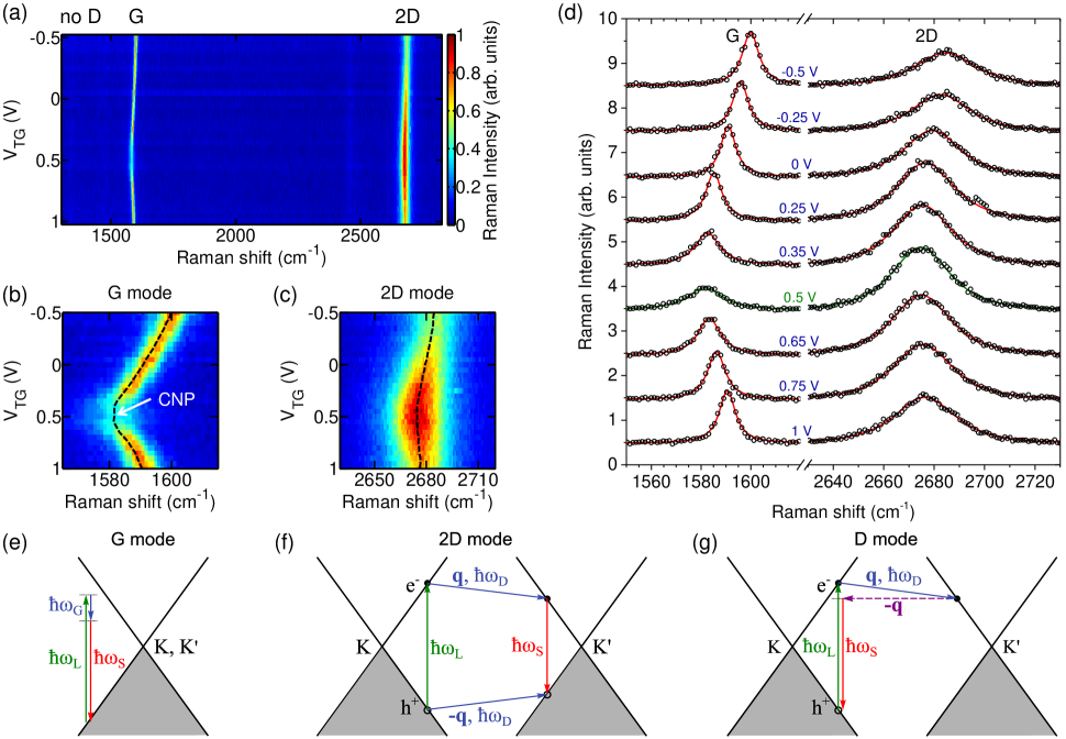
Figure 2 shows typical Raman spectra recorded over a top-gate voltage sweep, with the two prominent Raman features in pristine graphene: the first order G-mode feature, which involves zone-center optical phonons (at the point), and the second-order resonant 2D-mode feature, which involves near zone-edge optical phonons (at the K and K’ points).Malard et al. (2009); Ferrari and Basko (2013) Note that no defect-induced D-mode feature emerges from the background in our experimental conditions. This illustrates the high structural quality of the graphene sample. As expected,Das et al. (2008) the G-mode frequency and linewidth vary significantly with the top-gate bias (). Similar trends are observed by applying a back-gate voltage (). The minimum value of the G-mode frequency and the maximum value of its full width at half maximum (FWHM) are reached at the same value of . This value corresponds to the charge neutrality point (CNP), where . The CNP is reached at a finite , due to an unintentional doping of the graphene layer, induced by the substrate as well as the polymer electrolyte.Das et al. (2008) A finite value of results in a finite charge carrier density . In this work, a positive (negative) gate voltage corresponds to electron (hole) injection.111Throughout the manuscript, will refer to the electron density, such that positive (negative) correspond to electron (hole) doping. Qualitatively, for both positive and negative values of , we observe a nearly symmetric increase of accompanied by a symmetric decrease of (see Sec. V.1 for details). In contrast, the 2D-mode feature is less sensitive to doping than the G-mode feature Das et al. (2008) (see Sec. V.2).
In order to carefully study the G- and 2D-mode features as a function of , one has to convert the gate voltage into or, equivalently, . First, the Fermi energy at a given is , where is the reduced Planck’s constant and is the Fermi velocity of graphene on a SiO2 substrate.Knox et al. (2008) Note that this formula applies only at . However, in practice, finite temperature effects only induce a very minor correction to this simple scaling.Li et al. (2011) An applied top- or back-gate voltage creates an electrostatic potential difference between the graphene monolayer and the gate electrode. Besides, the injection of charge carriers in graphene leads to a shift of its Fermi energy. Consequently, introduces a difference in the electrochemical potentials of the gate electrode and of the graphene layer (see Fig. 1(c))
| (1) |
where is the elementary charge, is a constant that accounts for the initial doping and implicitly includes the work function difference between the two materials.Giovannetti et al. (2008)
Assuming that the gate can be modeled as a parallel plate capacitor with a geometrical gate capacitance , the relation between and is given by
| (2) |
Importantly, the first term on the right hand side of Eq. (2) scales as (i.e., ) and is related to the quantum capacitance of graphene ,Luryi (1988) while the second term scales as (i.e., as ) and is related to the geometrical gate capacitance . Das et al. (2008, 2009)
For a typical SiO2 back-gate insulator, the geometrical capacitance per unit area is simply given by , where is the relative permittivity of SiO2, the vacuum permittivity and is the SiO2 thickness. In this work, results in a back-gate capacitance . For a typical Fermi energy , the quantity is negligible as compared to the other term in Eq. (2).
The case of the polymer electrolyte top-gate is slightly more complicated. Indeed, when a voltage is applied between the gate and the SLG, Li+ and ClO diffuse in the polymer to form electrical double layers at the interfaces as it is sketched in Fig. 1(b).Das et al. (2008) These EDL can be modeled as parallel plate capacitors with a thickness given by the Debye length , and a geometrical capacitance per unit area . The total geometrical capacitance of the polymer electrolyte is thus given by where (resp. ) is the contact area between the polymer electrolyte and the gate electrode (resp. the graphene monolayer). Since (see Fig. 1(a)), one only needs to take into account the geometrical capacitance of the EDL at the graphene-polymer electrolyte interface. The Debye length is theoretically given by Das et al. (2008) , where is the temperature, is Boltzmann’s constant and is the concentration of ions in the polymer electrolyte. In practice, the exact value of cannot be measured. One can nevertheless obtain an estimate of , assuming a typical value of and for PEO.Das et al. (2008) This capacitance is more than two orders of magnitude larger than and becomes comparable to the quantum capacitance for . As a result, the two terms in Eq. (2) are of the same order of magnitude and must be taken into account in the present study.
IV Geometrical capacitance of the electrical double layer
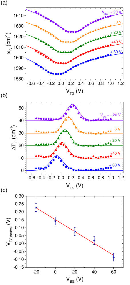
Our first objective is to precisely determine . Previous works on oxide dual-gated graphene FETs Meric et al. (2008); Xu et al. (2011a) have shown that provided one geometrical capacitance is known, the other can be determined by monitoring the minimum (source-drain) conductivity point as a function of the bottom and top-gate biases. At steady state, our dual-gated graphene FETs have the same equivalent electrical circuit (see Fig. 1(d)) as the devices of Ref. Xu et al., 2011a. Here, rather than using electron transport measurements, we apply micro-Raman scattering spectroscopy, which provides a local measurement. For a fixed , we sweep and record Raman spectra, as described in Sec. II.2. Then, we extract and from Lorentzian fits. Figures 3(a)-(b) show these two quantities as a function of for five different values of . We observe a clear shift of the CNP, attained at , with . In practice, is extracted from the curves, which, expectedly (see Sec. V.1), exhibit a sharper extremum near neutrality than the curves. As shown in Fig. 3(c), varies linearly with . Indeed, from the equivalent circuit in Fig. 1(d), the total charge density injected by top- and back-gates leads Xu et al. (2011a)
| (3) |
At the CNP, and . Therefore,
| (4) |
Using Eq. (4), a linear fit of the data in Fig. 3(c) yields . Since , we deduce that , which is of the same order of magnitude as what was reported before for similar devices.Das et al. (2008, 2009); Shimotani et al. (2006); Efetov and Kim (2010); Bruna et al. (2014) We may now convert into .
V Electron-phonon coupling in pristine graphene
V.1 Doping-dependence of the G-mode feature
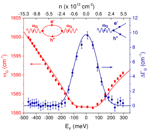
Considering only lattice expansion, due to the addition of charge carriers, one may expect the G-mode frequency to increase (decrease) under hole (electron) doping.Lazzeri and Mauri (2006) Thus, the peculiar, nearly symmetric behaviors observed here and previously reported by others Pisana et al. (2007); Yan et al. (2007); Das et al. (2008); Kalbac et al. (2010); Chen et al. (2011); Chattrakun et al. (2013) contrast strongly with the trends predicted if one only considers lattice expansion effects. This anomalous behavior has been originally predicted by Ando Ando (2006) and by Lazzeri and Mauri Lazzeri and Mauri (2006) as a consequence of the strong coupling between zone-center optical phonons and low-energy electronic excitations across the gapless bands of graphene. Related effects occur in metallic carbon nanotubes.Piscanec et al. (2007) The anomalous doping dependence of the G-mode can be described using the phonon self-energy,Ando (2006); Lazzeri and Mauri (2006); Pisana et al. (2007); Yan et al. (2007, 2008) the real part of which is equal to and the imaginary part to . As a result, the evolution of and are deeply connected (see Fig. 4).
The variation of is due to the decay of the G phonon into an electron-hole pair (see right inset in Fig. 4) and is given by
| (5) |
where is the phonon frequency at , is the Fermi-Dirac distribution at a temperature and is a dimensionless coefficient corresponding to the electron-phonon coupling strength222Here we choose to use the coupling constant as defined by Basko in Ref. Basko, 2008. In Refs. Lazzeri and Mauri, 2006; Pisana et al., 2007 the dimensionless electron-phonon coupling constant is denoted and is defined as (see also Sec. V.3). contains all other sources of broadening that are independent on the carrier density (anharmonic coupling,Bonini et al. (2007) disorder, instrument response function). For , vanishes due to Pauli blocking.
The evolution of with is the sum of an adiabatic contribution corresponding to the modification of the equilibrium lattice parameter and a non adiabatic one corresponding to the renormalization of the G-mode phonon energy due to interactions with virtual electron-hole pairs Ando (2006); Lazzeri and Mauri (2006) (see left inset in Fig. 4). At a finite temperature , the frequency shift is given byLazzeri and Mauri (2006); Pisana et al. (2007)
| (6) |
with
| (7) |
where denotes the Cauchy principal value. One should note that and are proportional to .
In the simulations described below, we use the results of the calculation by Lazzeri and Mauri to include adiabatic contribution (see Eq. (3) in Ref. Lazzeri and Mauri, 2006). Importantly, for , the adiabatic contribution provides only a minor correction to the non-adiabatic term and does not affect .
Moreover, to accurately describe the experimental evolution of the G mode, one also has to take into account random spatial fluctuations of the Fermi energy.Casiraghi et al. (2007); Martin et al. (2008); Xu et al. (2011b); Li et al. (2011) It is reasonable to assume that follows a Gaussian distribution Martin et al. (2008); Xu et al. (2011b); Li et al. (2011) around its mean value, with a standard deviation . Thereafter, the computed and used to fit our data are given by the convolution of this Gaussian distribution with Eq. (5) and (6).
Figure 3 displays the results of simultaneous fits of and for five top-gate sweeps at different . We used and the values of , and obtained in Sec. IV. Thus the fitting parameters are , and . The experimental data are remarkably well fitted by the theoretical model. Interestingly, although the two phonon anomaliesAndo (2006); Lazzeri and Mauri (2006); Yan et al. (2008) predicted at by Eq. (6) are largely smeared out at room temperature, one can still notice a hint of their presence in Fig. 3(a), 4 and 9(a).
From these five fits, we get and . Since on bare SiO2 without an electrochemical top-gate,Martin et al. (2008); Xue et al. (2011) we conclude that charge inhomogeneity does not have a major effect on our analysis. DFT calculations Lazzeri and Mauri (2006); Pisana et al. (2007) have predicted , which is slightly smaller, but consistent with our measurement.
Another way to further compare the experimental data and theory is to set as adjustable parameter when fitting and . This yields , and . These values are very consistent with the more constrained fits discussed above (see Sec. IV). Similar studies were repeated on more than five samples, with similar conclusions. This demonstrates that a direct fit of and can be used to get an accurate measurement of , which allows to convert into through Eq. (2). This is a much faster approach to determine , which does not require a dual-gated device. As an example, a fit of the data in Fig. 2 is shown in Fig. 4, and shows a very good agreement between experiment and theory. More generally, our fitting procedure allows us to estimate and with relative uncertainties of approximately and , respectively.
To better understand the importance to fit simultaneously and , we have fit these quantities separately for the measurements shown in Fig. 3 (not shown). From the fit of , we obtain , and . Except the large value of , the two parameters are reasonable. From the fit of , we obtain and and an unrealistically large . The latter value suggests that the behavior of can be rationalized using solely the quantum capacitance of graphene. This is understandable, since the variations of occur near , where the contribution of the quantum capacitance dominates in Eq. (2). However, the value of near is directly proportional to and is not influenced by , while varies mostly away from the CNP. Hence, its evolution with is influenced by both and . Consequently, a simultaneous fit allows for a reliable estimation of (through the doping dependence of ), and, in turn of (through the slope of curve, having constrained by ).
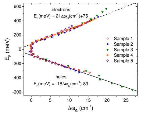
Figure 5 shows the evolution of as a function of for five different graphene FETs (denoted sample 1 to 5) in which and have been previously determined by the simultaneous fit of and . For these five samples, we found an average of and (see also Table 1). This translates into an average relative G-mode FWHM (see Eq. (5)) of (at , and ) that is consistent with the value of recorded on quasi-undoped suspended graphene at low temperature.Berciaud et al. (2013) Remarkably, and in spite of the different values of , the data for these five devices shown in Fig. 5 collapse onto a same curve. In practice, this very reproducible behavior can be used to evaluate knowing , which is of broad interest in graphene science. For this purpose, we consider the asymptotic behavior of . When , Eq. (7) becomes
| (8) |
Assuming that the adiabatic contribution is negligible compared to , should be linear with . Indeed, in Fig. 5 for the five different samples, clearly scales linearly for . The slightly different slopes observed for electron and hole doping arise from the opposite sign of the adiabatic corrections.
For , we find
| (9) | |||||
| (10) |
where is expressed in meV and in . However, it should be noted that this linear scaling only holds for . In fact, for higher , no longer scales linearly with since can no longer be neglected compared to . Moreover, Eqs. (9) and (10) can be applied provided the shift in is exclusively due to doping, i.e., other extrinsic factors, such as mechanical strain do not contribute. If this is not the case, one has to separate the various contributions, using, e.g. the method described in Ref. Lee et al., 2012a with the results of Sec. VII.2.
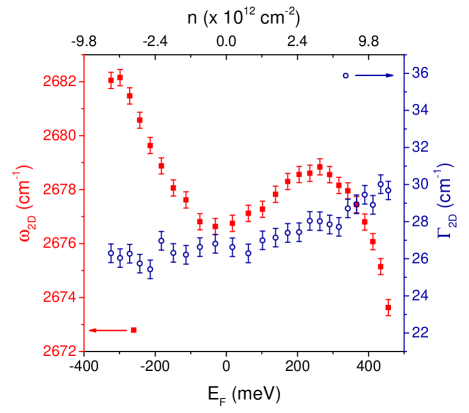
V.2 Doping-dependence of the 2D-mode feature
Let us briefly comment on the 2D-mode feature. Figure 6 shows the evolution of the frequency and FWHM of the 2D-mode feature with for sample 2 (2D mode spectra are also shown for sample 1 in Fig. 2). In supported graphene, the 2D-mode feature typically exhibit a quasi-symmetric lineshape that can be phenomenologically fit to a modified Lorentzian profile.Basko (2008); Berciaud et al. (2013) We find that does not vary significantly with the gate bias, while varies little at moderate doping , but tends to stiffen (soften) significantly for stronger hole (electron) doping. The observed evolution of outlined in Fig. 6 (see also Figs. 2 and 9) can be qualitatively understood as the sum of a dominant adiabatic contribution and a weaker non-adiabatic contribution. The latter is reduced as compared to the case of the G-mode feature, likely because the 2D-mode feature involves phonons that are significantly away from the edges of the Brillouin zone.Das et al. (2008)
V.3 Electron-electron and electron-phonon scattering
Another useful quantity is the integrated intensity of a Raman feature (denoted ), which represents the total probability of the Raman scattering process. The integrated intensity of the 2D-mode feature () depends on ,Das et al. (2008, 2009); Basko et al. (2009) whereas does not, as long as , where is the energy of the incident laser.Basko (2009); Kalbac et al. (2010); Chen et al. (2011) In Fig. 7, we consider the ratio , which is maximum for and decreases almost symmetrically for increasing . Following Ref. Basko, 2008; Basko et al., 2009, the integrated intensity of the 2D-mode feature writes
| (11) |
where is the total electron scattering rate, with the electron-phonon scattering rate, the electron-defect scattering rate, and the electron-electron scattering rate. The electron-phonon scattering rate can be approximated as , where and are the scattering rates for zone-edge and zone-center optical phonons, respectively. Note that Eq. (11) is obtained under the assumption of a fully resonant process (see Fig. 2(f)), and that trigonal warping effects leading to momentum-dependent scattering rates are neglected.Basko (2008); Basko et al. (2009); Basko (2013); Venezuela et al. (2011) While and do not depend on , has been predicted to scale linearly with . For , Basko et al. calculatedBasko et al. (2009)
| (12) |
where corresponds to the value at .
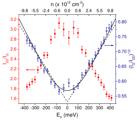
In this section, we are considering pristine graphene, in which . As illustrated by the dashed line in Fig. 7, our experimental data agree well with a fit based on Eq. (12) for . However, we observe a deviation from Eq. (12) near the CNP, likely due to Fermi energy fluctuations. As in Sec. V.1, we therefore fit the experimental data with the Gaussian convolution of Eq. (12), resulting in the solid line in Fig. 7. The agreement between theory and experiment is very good and more compelling than in the seminal study in Ref. Basko et al., 2009. The fitting parameters are , and . We repeated this analysis on three pristine samples and found average values of , and (see Table 1). Note that the dispersion of the measurements on these three devices is very similar to the dispersion observed when measuring on several spots on the same sample. The value of is in good agreement with the estimate in Ref. Basko et al., 2009. The Fermi energy fluctuation obtained here is more realistic than the lower values estimated from the simultaneous fit of and (see Sec. V.1). It corresponds to a charge inhomogeneity of , in line with previous scanning tunneling microscopy measurements.Martin et al. (2008); Xue et al. (2011)
Interestingly, in Ref. Basko et al., 2009, the authors claim that the intrinsic value of for undoped graphene is in the range 12-17 (using a 514.5 nm excitation wavelength). However, this estimation is based on Raman measurements on quasi-undoped suspended grapheneBerciaud et al. (2009) and does not take into account the effect of optical interferences, which occur in graphene-based multilayer structures and may critically affect the intensity of the Raman features.Yoon et al. (2009); Metten et al. (2014) From the data in Ref. Metten et al., 2014, an intrinsic value corrected from interference effects of can be estimated for freely suspended, undoped graphene, using a 532 nm excitation wavelength, as in the present study. Considering the distinct Raman enhancement factors for the G- and 2D-mode features in the PEO/graphene/SiO/Si multilayer structure, our average value of translates into an average intrinsic value of (see Table 1), which is in excellent agreement with our estimate on suspended graphene.
As outlined in Ref. Basko, 2008; Basko et al., 2009; Basko and Aleiner, 2008, the scattering rate is linked to the dimensionless electron-phonon coupling constants and through
| (13) |
where is the in-plane transverse optical (TO) phonon energy at the K (K’) point, is the in-plane optical phonon energy at (i.e., the G-mode frequency) and is the laser photon energy.
For sample 2 (see Fig. 7 and Table 1), a value of is deduced from the simultaneous fits of and (see Sec. V.1). Then, using Eq. (13), we can estimate333Following Refs. Basko et al., 2009; Basko and Aleiner, 2008, the value of deduced from Eq. (13) corresponds to the electron-phonon coupling constant at a carrier energy of . To obtain the coupling constant exactly at the K point , we can use the relation that is valid for a polymer electrolyte with a relative permittivity . In this manuscript, implicitly denotes . . Overall, for the three pristine samples studied here, we obtained average values of , and (see Table 1).
To close this section, we compare the average ratio deduced from our doping-dependent Raman study to a direct estimate derived from the measured ratio of the integrated intensities of the intravalley (2D’ mode) and intervalley (2D mode) resonant two-phonon features.Ferrari and Basko (2013) This ratio is expected to be independent of and writesBasko (2008); Basko et al. (2009) . In our experimental conditions, we obtain . Thus, by considering one more time the different Raman enhancement factors for the 2D- and 2D’-mode features in the PEO/graphene/SiO/Si multilayer system, we deduce . This value is consistent with the analysis outlined above.
| Sample | ||||||
|---|---|---|---|---|---|---|
| 1 (without defects) | 5.6 | - | 50 | 0.027 | 0.17 | |
| 1 (with defects) | 4.6 | 1.7 | 0.9 | 57 | 0.031 | |
| 2 (without defects) | 4.2 | - | 51 | 0.034 | 0.17 | |
| 2 (with defects) | 3.3 | 1.3 | 0.7 | 69 | 0.031 | |
| 3 | 5.0 | - | 39 | 0.031 | 0.12 | |
| 4 | 4.4 | 2.6 | 1.4 | 53 | 0.037 | |
| 5 | 4.3 | 1.4 | 0.7 | 72 | 0.031 |
VI Defective graphene
VI.1 Creation of defects
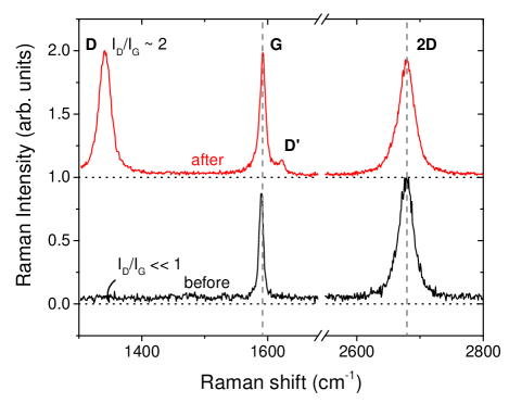
As mentioned in Sec. II, when an electrochemically gated graphene FET is subjected to a sufficiently high gate bias, electrochemical reactions may occur Kalbac et al. (2010); Efetov and Kim (2010); Bruna et al. (2014) and create defects in the graphene channel. In our devices, a reaction systematically occurs at negative gate biases ( to ). The threshold voltage depends on the sample and on the gate capacitance. Electrochemical reactions result in an increase of the gate leak current above , and in the emergence of defect-induced features in the Raman spectrum. Figure 8 shows two Raman spectra recorded at on sample 1, before applying any gate voltage and after an electrochemical reaction has taken place. We clearly see that (i) the G- and 2D-mode features do not shift, and (ii) prominent D- and D’-mode features develop. These two Raman modes are known to be forbidden by symmetry and can only be observed in the presence of defects. Ferrari and Robertson (2000); Thomsen and Reich (2000b); Maultzsch et al. (2004); Malard et al. (2009); Ferrari and Basko (2013)
VI.2 Doping dependence of the Raman features in defective graphene
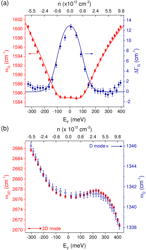
Figure 9(a) shows and in defective graphene. By comparing this figure with Fig. 4, we conclude that the doping dependence of the G-mode feature is not affected by the presence of defects. Both and are well fit to the theoretical model of Sec. V.1. The frequencies and are also shown as a function of in Fig. 9(b). The D- and 2D-mode features are fit to a modified Lorentzian profile.Basko (2008); Berciaud et al. (2013) We note that both frequencies follow identical trends. More precisely . The factor 2 is expected, since the 2D mode is the two-phonon overtone of the D-mode (in the D-mode process, one inelastic scattering by a near zone-edge TO phonon is replaced by an elastic scattering by a defect Thomsen and Reich (2000b); Basko (2008); Venezuela et al. (2011)). This small difference between and is consistently observed in all the studied samples. It could be due to slight differences in the resonance conditions.Martins Ferreira et al. (2010); Venezuela et al. (2011); Ferrari and Basko (2013)
VI.3 Electron-defect scattering
In Sec. V.3, using Eq. (12), we have shown that it is possible to deduce the phonon scattering rate in pristine graphene from the study of the integrated intensities of the G- and 2D-mode features. In defective graphene, a similar analysis can be performed provided that a finite electron-defect scattering rate , proportional to the defect concentration , is taken into consideration.Venezuela et al. (2011); Bruna et al. (2014)
In Fig. 10(a), we plot as a function of . The data is extracted from another series of measurements in sample 1, at a same spot, before and after the creation of defects. As expected, we observe that the two datasets are well fitted by Eq. (12). The fitting parameters are , , for pristine graphene, and , , , for defective graphene, respectively.
Since is not affected by the presence of defects, we can estimate that for sample 1. Thus, although the D- and 2D-mode features have similar integrated intensities (, as shown in Fig. 10(b)), , as predicted in the low-defect concentration regime Venezuela et al. (2011) (see also Sec. VI.4). Another way to determine is to compare the quantity , in the presence and in the absence of defects. According to Eq. (11) and (12), one obtains
| (14) |
The results of Fig. 10(a) indeed show that , in agreement with Eq. (14). From the fitting parameters, we estimate that , in good agreement with the other estimate obtained above.
To conclude this subsection, we focus on the dependence of on . In practice, is routinely used to estimate a defect concentration.Tuinstra and Koenig (1970); Ferrari and Robertson (2000); Martins Ferreira et al. (2010); Lucchese et al. (2010); Cançado et al. (2011); Eckmann et al. (2013); Ferrari and Basko (2013); Beams et al. (2015) However, although it is not fully resonant, the D mode may involve one resonant electron-phonon scattering process Thomsen and Reich (2000a); Maultzsch et al. (2004); Ferrari and Basko (2013); Venezuela et al. (2011); Beams et al. (2015) (see Fig. 2(g)). In other words, similarly to , is also expected to decrease with increasing . In Fig. 10(b), we show , and as a function of , while Fig. 10(c) displays and as a function of . Clearly, and show a very similar doping dependence (see also Ref. Bruna et al., 2014). More quantitatively, a phenomenological fit of using Eq. (12) (applied to instead of ) agrees well with our measurements (see Fig. 10(c)) and yields , , and . The value of is very close to that obtained by fitting .
We note that Ref. Bruna et al., 2014 report a value of similar to ours (see Table 1), for defective graphene samples with slightly larger, yet similar values of . However, a larger value of is estimated, using the value of extracted from the measurements in Ref. Basko et al., 2009. Our work provides an estimate of from a series of measurements performed on a same sample and suggests that , even for . Consequently, in defective graphene, we consider that the slope of the curve provides a fair estimate of , from which we extract , knowing . Albeit the existence of a finite presumably leads to a slight overestimation of , we do not observe a large difference between the values measured on defective and on pristine graphene (see Table 1). More quantitatively, by averaging on four defective graphene samples with similar defect concentrations, we obtain , a value that is indeed slightly larger than the average obtained on three pristine samples (see Table 1 and Sec. V.3).
VI.4 Defect concentration
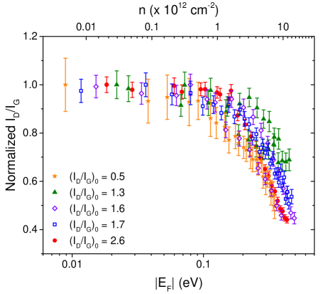
In principle, the concentration of defects in a graphene sample can be deduced from the analysis of the defect-induced Raman modes, such as the (intervalley) D mode or the (intravalley) D’ mode. The study of the defect-induced Raman modes has far reaching consequences for sample characterization and can also be a very useful tool to monitor chemical reactions on graphene. Following the seminal work by Tuinstra and Koenig,Tuinstra and Koenig (1970) several groups have proposed analytical expressions to connect and in various graphitic materials, from weakly defective graphene layers to amorphous carbon.Tuinstra and Koenig (1970); Ferrari and Robertson (2000); Martins Ferreira et al. (2010); Lucchese et al. (2010); Cançado et al. (2011)
The defective graphene samples studied here exhibit an integrated intensity ratio near the CNP (see Fig. 8 and 11, and Table 1). Their Raman features show only a slight spectral broadening (by a few ) compared to the pristine case (see Fig. 8). More precisely, we find, for five series of gate-dependent measurements on various defective regions, that (as compared to for pristine graphene), and . Following the three stage classification of Ref. Ferrari and Robertson, 2000 and related works,Martins Ferreira et al. (2010); Lucchese et al. (2010); Cançado et al. (2011); Eckmann et al. (2013) such samples can be described as stage 1, i.e., still in the weakly defective regime. Let us assume point defects, separated by an average distance . In this regime, Eq. (9) of Ref. Martins Ferreira et al., 2010 and the results of Ref. Cançado et al., 2011 provide the relation444We note that since the D- and G-mode frequencies are relatively close, the impact of interference effects on the ratio is negligible in our experimental conditions.Yoon et al. (2009)
| (15) |
where is the concentration of defects in cm-2, is in nm, is the laser photon energy in eV and is taken at , still with Fermi energy fluctuations. According to Ref. Eckmann et al., 2013, the scaling introduced in Eq. (15) is independent of the type of defect.
In Fig. 11, we plot , normalized by its value at for five different sets of measurements (including some at different locations on the same sample), with different defect concentrations. We observe that all the data collapse onto the same curve. For , and this ratio decreases by less than for . Thus, since unintentional doping in graphene samples typically leads to , the experimentally measured can be used together with Eq. (15) for an estimation of in weakly doped samples.
Using Eq. (15), the electrochemically-induced defect concentrations deduced for our measurements (see Table 1 and Fig. 11) range from to . This translates into ranging from 19.5 nm down to 8.5 nm. The latter value is at the limit of the weakly defective regime, which assumes .
Overall, the results shown in Figs. 9-11 demonstrate that for defect concentrations below approximately , the electron-defect scattering rate remains much smaller than the electron-phonon scattering rate, and that the doping dependence of the G- and 2D-mode features is essentially the same as in pristine graphene. These results contrast with the fact that even for relatively low in the range , the integrated intensity of the D-mode feature is smaller, yet on the same order of magnitude as that of the 2D-mode feature, in keeping with recent experimentalMartins Ferreira et al. (2010); Bruna et al. (2014) and theoretical results.Venezuela et al. (2011) This calls for further investigations of the integrated intensity of the one-phonon, defect-induced Raman features relative to that of their symmetry-allowed overtones.
VII Correlations
In the previous sections, we have successfully compared our measurements to theoretical calculations and, in particular estimated the electron-phonon coupling constants. In this section, we present correlations between the frequencies and linewidths of the main Raman features in doped graphene, with the aim to extract universal behaviors that could be useful for sample characterization. Based on the conclusions of Sec. VI, the correlations discussed in the following will also hold in weakly defective graphene.
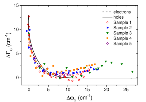
VII.1 G-mode frequency and linewidth
Figure 12 shows as a function of for the five different samples already shown in Fig. 5. We observe a universal behavior and the experimental data are in good agreement with the theoretical calculations, although the very slight difference expected for electron and hole doping (due to , see Eq. (6)) is not resolved experimentally, likely due to Fermi energy fluctuations. We also note that in the high-doping regime, tends to increase somewhat. This increase, also observed by others,Bruna et al. (2014) is presumably due to the increasing inhomogeneity of the charge distribution at high top-gate biases. The correlation displayed in Fig. 12 may also be used to estimate , especially in the low doping regime .
VII.2 G- and 2D-mode frequencies
Figure 13 represents the evolution of as a function of for the same five samples. A clear correlation is observed between these two quantities. For hole doping, the correlation is quasi-linear in the range of studied here . In contrast, for electron doping, a quasi-linear scaling, again with a (much smaller) positive slope is also observed at low doping , until levels off and ultimately decreases, leading to a non-linear scaling. This behavior was observed on every sample either for electrolyte-gated or conventional back-gated FETs and has been also observed in chemically doped graphene.Lee et al. (2012a)
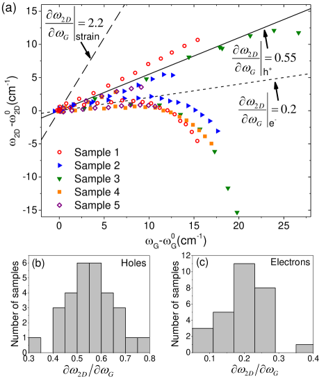
From the slopes extracted on approximately thirty samples (see Fig. 13(b)-(c)), we find an average of for hole doping and of for electron doping, respectively. The former value agrees well with the slope of extracted numerically by Lee et al.Lee et al. (2012a) from the data in Ref. Das et al., 2008, 2009. From our statistical study, we note that the correlation between and is more dispersed than the correlation between and . This is chiefly due to the dependence of on , which is not as universal as that of . In addition, it is rather challenging to extract a well-defined correlation for electron doping due to the small variations of at moderate doping.
Noteworthy, estimations of based on the frequency and/or linewidth of the Raman features may only be reliable if graphene is not subjected to significant strains. Indeed, is marginally affected by isotropic strains below .Metten et al. (2014) However, the G-mode feature may broaden and ultimately split into two sub-features in the presence of larger anisotropic strains.Mohiuddin et al. (2009); Huang et al. (2009) In addition, the Raman features soften (stiffen) under tensile (compressive) strain. A linear correlation between and has been measured in strained graphene.Lee et al. (2012a); Zabel et al. (2011); Lee et al. (2012b); Metten et al. (2013, 2014) Since the measured slopes (, for undoped, strained graphene Metten et al. (2014)) are appreciably larger than the slopes measured in doped graphene (presumably under a small but constant built-in strain), Lee et al. have proposed to use the correlation between and as a robust tool to optically separate strain from charge doping.Lee et al. (2012a)
Following Ref. Lee et al., 2012a, we may then define three vectors corresponding to the slopes , under strain, hole and electron doping, respectively (see Fig. 13). To further deduce absolute levels of strain and/or doping, one also has to know the 2D- and G-mode frequencies that corresponds to an undoped and unstrained graphene sample. For clarity, in Fig. 13, the 2D- and G-mode frequencies are shown relative to the measurements at . These origin points, denoted (, ) might differ from the reference point corresponding to undoped and unstrained graphene, since an undetermined amount of native strain may be present and induce a shift along the strain vector.
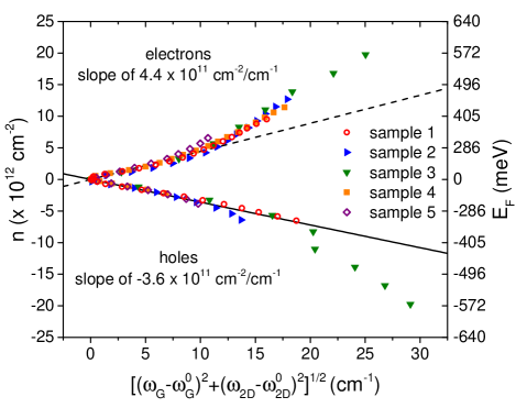
The data in Fig. 13 allows an estimation of the coefficient which connects , the measured distance from the zero doping point, to a given doping level (see Fig. 14). We chose to consider instead of because it is a more relevant quantity as far as graphene characterization is concerned. Although the curves displayed in Fig. 14 are not expected to exhibit a linear scaling (as opposed to the data shown in Fig. 5), we observe a quasi-linear scaling for sufficiently small doping (). We therefore fit the linear part for both electron- and hole-doping with a line intercepting the zero doping point. We find slopes of for electrons and for holes, respectively.
Finally, considering the Grüneisen parameters of 1.8 and 2.4 for the Raman G- and 2D-modes under isotropic strain,Metten et al. (2014) we can estimate a slope of to connect to an applied isotropic strain. In practice, the strain field may be anisotropic, depending on the sample and on the experimental conditions, leading to a different slope. These coefficients may be used for a reliable estimation of doping and strain in graphene samples and devices.
VIII Conclusion
We have presented a robust method, based on Raman scattering spectroscopy, to accurately determine the geometrical capacitance, and hence, the Fermi energy in electrochemically-gated graphene field-effect transistors with a spatial resolution down to approximately . Such a calibration allows for quantitative analysis of the doping dependence of the frequency, linewidth and integrated intensity of the main Raman features. The anomalous doping dependence of the G-mode phonons is well captured by theoretical models over a broad range of Fermi energies above or below the Dirac point, and provides an experimental measurement of the electron-phonon coupling constant at the point of the Brillouin zone. We have then exploited the peculiar doping dependence of the integrated intensity of the multiphonon resonant Raman features, in particular the resonant 2D-mode feature, to estimate the electron-phonon coupling constant at the edges (K, K’) of the Brillouin zone. Finally, from the doping dependence of the integrated intensity of the defect-induced D-mode feature, we can estimate the electron-defect scattering rate in stage 1 defective graphene samples.
Our study provides useful guidelines for the characterization of graphene samples. We have, in particular, considered the correlation between the frequency and width of the G-mode feature, as well as between the frequencies of the 2D- and G-mode features. These correlations reveal universal behaviors that can therefore be applied to evaluate doping in a variety of experimental situations. We have also demonstrated that defects can be efficiently created in-situ in electrochemically gated graphene field effect transistors. The integrated intensity of the D-mode feature decreases monotonically with increasing doping, and follows the same scaling as that of its two-phonon overtone. However, due to Fermi energy fluctuations, the D-mode intensity is nearly constant for Fermi energy shifts below 200 meV relative to the Dirac point, which is of practical interest for the determination of the defect concentration.
In the present work, we conservatively estimate that Fermi energies as high as above the Dirac point can be achieved in ambient conditions, without damaging graphene. This naturally opens exciting perspectives for optoelectronics. Nevertheless, a well controlled Raman scattering study of the crossover between the intermediate doping regime achieved here and the very high doping regime remains elusive. Finally, electrochemical gating is a promising strategy to investigate electron-phonon coupling in other two-dimensional materials, including transition metal dichalcogenides.Chakraborty et al. (2012)
Acknowledgements.
We wish to thank G. Weick for his careful proofreading of the manuscript and for fruitful discussions. We are also grateful to D. M. Basko, F. Mauri, F. Federspiel, D. Metten, S. Zanettini and B. Doudin for discussions. We thank A. Mahmood, F. Godel, S. Kuppusamy, F. Chevrier, A. Boulard and M. Romeo for technical support, as well as R. Bernard, S. Siegwald, and H. Majjad for help with sample preparation in the StNano clean room facility. We acknowledge support from the Agence Nationale de la Recherche (under grant QuanDoGra 12 JS10-001-01), from the CNRS and from Université de Strasbourg.References
- Novoselov et al. (2004) K. S. Novoselov, A. K. Geim, S. V. Morozov, D. Jiang, Y. Zhang, S. V. Dubonos, I. V. Grigorieva, and A. A. Firsov, “Electric field effect in atomically thin carbon films,” Science 306, 666–669 (2004).
- Zhang et al. (2005) Y. Zhang, Y.-W. Tan, H. L. Stormer, and P. Kim, “Experimental observation of the quantum Hall effect and Berry’s phase in graphene,” Nature 438, 201–204 (2005).
- Novoselov et al. (2005) K. S. Novoselov, A. K. Geim, S. V. Morozov, D. Jiang, M. I. Katsnelson, I. V. Grigorieva, S. V. Dubonos, and A. A. Firsov, “Two-dimensional gas of massless Dirac fermions in graphene,” Nature 438, 197 – 200 (2005).
- Wang et al. (2008) F. Wang, Y. Zhang, C. Tian, C. Girit, A. Zettl, M. Crommie, and Y.R. Shen, “Gate-variable optical transitions in graphene,” Science 320, 206–209 (2008).
- Li et al. (2008) Z. Q. Li, E. A. Henriksen, Z. Jiang, Z. Hao, M. C. Martin, P. Kim, H. L. Stormer, and D. N. Basov, “Dirac charge dynamics in graphene by infrared spectroscopy,” Nature Physics 4, 532–535 (2008).
- Mak et al. (2014) Kin Fai Mak, Felipe H. da Jornada, Keliang He, Jack Deslippe, Nicholas Petrone, James Hone, Jie Shan, Steven G. Louie, and Tony F. Heinz, “Tuning many-body interactions in graphene: The effects of doping on excitons and carrier lifetimes,” Physical Review Letters 112, 207401 (2014).
- Yan et al. (2007) Jun Yan, Yuanbo Zhang, Philip Kim, and Aron Pinczuk, “Electric field effect tuning of electron-phonon coupling in graphene,” Physical Review Letters 98, 166802 (2007).
- Pisana et al. (2007) Simone Pisana, Michele Lazzeri, Cinzia Casiraghi, Kostya S. Novoselov, A. K. Geim, Andrea C. Ferrari, and Francesco Mauri, “Breakdown of the adiabatic born-oppenheimer approximation in graphene,” Nature Materials 6, 198–201 (2007).
- Novoselov et al. (2012) K. S. Novoselov, V. I. Fal′ko, L. Colombo, P. R. Gellert, M. G. Schwab, and K. Kim, “A roadmap for graphene,” Nature 490, 192–200 (2012).
- Malard et al. (2009) L. M. Malard, M. A. Pimenta, G. Dresselhaus, and M. S. Dresselhaus, “Raman spectroscopy in graphene,” Physics Reports 473, 51 – 87 (2009).
- Ferrari and Basko (2013) Andrea C. Ferrari and Denis M. Basko, “Raman spectroscopy as a versatile tool for studying the properties of graphene,” Nature Nanotechnology 8, 235–246 (2013).
- Berciaud et al. (2010) Stéphane Berciaud, Melinda Y. Han, Kin Fai Mak, Louis E. Brus, Philip Kim, and Tony F. Heinz, “Electron and optical phonon temperatures in electrically biased graphene,” Physical Review Letters 104, 227401 (2010).
- Chae et al. (2010) Dong-Hun Chae, Benjamin Krauss, Klaus von Klitzing, and Jurgen H. Smet, “Hot phonons in an electrically biased graphene constriction,” Nano Letters 10, 466–471 (2010).
- Freitag et al. (2010) M. Freitag, H.-Y. Chiu, M. Steiner, V. Perebeinos, and P. Avouris, “Thermal infrared emission from biased graphene,” Nature Nanotechnology 5, 497–501 (2010).
- Basko et al. (2009) D. M. Basko, S. Piscanec, and A. C. Ferrari, “Electron-electron interactions and doping dependence of the two-phonon Raman intensity in graphene,” Physical Review B 80, 165413 (2009).
- Bruna et al. (2014) Matteo Bruna, Anna K. Ott, Mari Ijäs, Duhee Yoon, Ugo Sassi, and Andrea C. Ferrari, “Doping dependence of the Raman spectrum of defected graphene,” ACS Nano 8, 7432–7441 (2014).
- Liu et al. (2013) Junku Liu, Qunqing Li, Yuan Zou, Qingkai Qian, Yuanhao Jin, Guanhong Li, Kaili Jiang, and Shoushan Fan, “The dependence of graphene Raman d-band on carrier density,” Nano Letters 13, 6170–6175 (2013).
- Casiraghi et al. (2007) C. Casiraghi, S. Pisana, K. S. Novoselov, A. K. Geim, and A. C. Ferrari, “Raman fingerprint of charged impurities in graphene,” Applied Physics Letters 91, 233108 (2007).
- Berciaud et al. (2009) Stéphane Berciaud, Sunmin Ryu, Louis E. Brus, and Tony F. Heinz, “Probing the intrinsic properties of exfoliated graphene: Raman spectroscopy of free-standing monolayers,” Nano Letters 9, 346–352 (2009).
- Ni et al. (2009) Zhen Hua Ni, Ting Yu, Zhi Qiang Luo, Ying Ying Wang, Lei Liu, Choun Pei Wong, Jianmin Miao, Wei Huang, and Ze Xiang Shen, “Probing charged impurities in suspended graphene using Raman spectroscopy,” ACS Nano 3, 569–574 (2009).
- Ryu et al. (2010) Sunmin Ryu, Li Liu, Stéphane Berciaud, Young-Jun Yu, Haitao Liu, Philip Kim, George W. Flynn, and Louis E. Brus, “Atmospheric oxygen binding and hole doping in deformed graphene on a SiO2 substrate,” Nano Letters 10, 4944–4951 (2010).
- Jung et al. (2009) Naeyoung Jung, Namdong Kim, Steffen Jockusch, Nicholas J. Turro, Philip Kim, and Louis Brus, “Charge transfer chemical doping of few layer graphenes: Charge distribution and band gap formation,” Nano Letters 9, 4133–4137 (2009).
- Zhao et al. (2010) WeiJie Zhao, PingHeng Tan, Jun Zhang, and Jian Liu, “Charge transfer and optical phonon mixing in few-layer graphene chemically doped with sulfuric acid,” Physical Review B 82, 245423 (2010).
- Jung et al. (2011) Naeyoung Jung, Bumjung Kim, Andrew C. Crowther, Namdong Kim, Colin Nuckolls, and Louis Brus, “Optical reflectivity and Raman scattering in few-layer-thick graphene highly doped by K and Rb.” ACS Nano 5, 5708–5716 (2011).
- Howard et al. (2011) C. Howard, M. Dean, and F. Withers, “Phonons in potassium-doped graphene: The effects of electron-phonon interactions, dimensionality, and adatom ordering,” Physical Review B 84, 241404 (2011).
- Crowther et al. (2012) Andrew C. Crowther, Amanda Ghassaei, Naeyoung Jung, and Louis E. Brus, “Strong charge-transfer doping of 1 to 10 layer graphene by NO2,” ACS Nano 6, 1865–1875 (2012).
- Parret et al. (2013) Romain Parret, Matthieu Paillet, Jean-Roch Huntzinger, Denise Nakabayashi, Thierry Michel, Antoine Tiberj, Jean-Louis Sauvajol, and Ahmed A. Zahab, “In situ Raman probing of graphene over a broad doping range upon rubidium vapor exposure,” ACS Nano 7, 165–173 (2013).
- Chen et al. (2014) Zheyuan Chen, Pierre Darancet, Lei Wang, Andrew C. Crowther, Yuanda Gao, Cory R. Dean, Takashi Taniguchi, Kenji Watanabe, James Hone, Chris A. Marianetti, and Louis E. Brus, “Physical adsorption and charge transfer of molecular Br2 on graphene,” ACS Nano 8, 2943–2950 (2014).
- McChesney et al. (2010) J. L. McChesney, Aaron Bostwick, Taisuke Ohta, Thomas Seyller, Karsten Horn, J. González, and Eli Rotenberg, “Extended van hove singularity and superconducting instability in doped graphene,” Physical Review Letters 104, 136803 (2010).
- Profeta et al. (2012) Gianni Profeta, Matteo Calandra, and Francesco Mauri, “Phonon-mediated superconductivity in graphene by lithium deposition,” Nature Physics 8, 131–134 (2012).
- Nandkishore et al. (2012) Rahul Nandkishore, L. S. Levitov, and A. V. Chubukov, “Chiral superconductivity from repulsive interactions in doped graphene,” Nature Physics 8, 158–163 (2012).
- Ma et al. (2010) Tianxing Ma, Feiming Hu, Zhongbing Huang, and Hai-Qing Lin, “Controllability of ferromagnetism in graphene,” Applied Physics Letters 97, 112504 (2010).
- Li et al. (2010) Guohong Li, A. Luican, J. M. B. Lopes dos Santos, A. H. Castro Neto, A. Reina, J. Kong, and E. Y. Andrei, “Observation of van hove singularities in twisted graphene layers,” Nature Physics 6, 109–113 (2010).
- Makogon et al. (2011) D. Makogon, R. van Gelderen, R. Roldán, and C. Morais Smith, “Spin-density-wave instability in graphene doped near the van hove singularity,” Physical Review B 84, 125404 (2011).
- Koppens et al. (2011) Frank H. L. Koppens, Darrick E. Chang, and F. Javier García de Abajo, “Graphene plasmonics: A platform for strong light–matter interactions,” Nano Letters 11, 3370–3377 (2011).
- García de Abajo (2014) F. Javier García de Abajo, “Graphene plasmonics: Challenges and opportunities,” ACS Photonics 1, 135–152 (2014).
- Yan et al. (2008) Jun Yan, Erik Henriksen, Philip Kim, and Aron Pinczuk, “Observation of anomalous phonon softening in bilayer graphene,” Physical Review Letters 101, 136804 (2008).
- Araujo et al. (2012) P. Araujo, D. Mafra, K. Sato, R. Saito, J. Kong, and M. Dresselhaus, “Phonon self-energy corrections to nonzero wave-vector phonon modes in single-layer graphene,” Physical Review Letters 109, 046801 (2012).
- Lu et al. (2004) Chenguang Lu, Qiang Fu, Shaoming Huang, and Jie Liu, “Polymer electrolyte-gated carbon nanotube field-effect transistor,” Nano Letters 4, 623–627 (2004).
- Kim et al. (2013) Se Hyun Kim, Kihyon Hong, Wei Xie, Keun Hyung Lee, Sipei Zhang, Timothy P. Lodge, and C. Daniel Frisbie, “Electrolyte-gated transistors for organic and printed electronics,” Advanced Materials 25, 1822–1846 (2013).
- Das et al. (2008) A. Das, S. Pisana, B. Chakraborty, S. Piscanec, S. K. Saha, U. V. Waghmare, K. S. Novoselov, H. R. Krishnamurthy, A. K. Geim, A. C. Ferrari, and A. K. Sood, “Monitoring dopants by Raman scattering in an electrochemically top-gated graphene transistor,” Nature Nanotechnology 3, 210–215 (2008).
- Efetov and Kim (2010) Dmitri K. Efetov and Philip Kim, “Controlling electron-phonon interactions in graphene at ultrahigh carrier densities,” Physical Review Letters 105, 256805 (2010).
- Yan et al. (2009) Jun Yan, Theresa Villarson, Erik Henriksen, Philip Kim, and Aron Pinczuk, “Optical phonon mixing in bilayer graphene with a broken inversion symmetry,” Physical Review B 80, 241417 (2009).
- Das et al. (2009) A. Das, B. Chakraborty, S. Piscanec, S. Pisana, A. K. Sood, and A. C. Ferrari, “Phonon renormalization in doped bilayer graphene,” Physical Review B 79, 155417 (2009).
- Kalbac et al. (2010) Martin Kalbac, Alfonso Reina-Cecco, Hootan Farhat, Jing Kong, Ladislav Kavan, and Mildred S. Dresselhaus, “The influence of strong electron and hole doping on the Raman intensity of chemical vapor-deposition graphene,” ACS Nano 4, 6055–6063 (2010).
- Chen et al. (2011) Chi-Fan Chen, Cheol-Hwan Park, Bryan W. Boudouris, Jason Horng, Baisong Geng, Caglar Girit, Alex Zettl, Michael F. Crommie, Rachel A. Segalman, Steven G. Louie, and Feng Wang, “Controlling inelastic light scattering quantum pathways in graphene,” Nature 471, 617–620 (2011).
- Chattrakun et al. (2013) Kanokporn Chattrakun, Shengqiang Huang, K. Watanabe, T. Taniguchi, A. Sandhu, and B. J. LeRoy, “Gate dependent Raman spectroscopy of graphene on hexagonal boron nitride,” Journal of Physics: Condensed Matter 25, 505304 (2013).
- Mak et al. (2009) Kin Fai Mak, Chun Hung Lui, Jie Shan, and Tony F. Heinz, “Observation of an electric-field-induced band gap in bilayer graphene by infrared spectroscopy,” Physical Review Letters 102, 256405 (2009).
- Zhang et al. (2009) Yuanbo Zhang, Tsung-Ta Tang, Caglar Girit, Zhao Hao, Michael C. Martin, Alex Zettl, Michael F. Crommie, Y. Ron Shen, and Feng Wang, “Direct observation of a widely tunable bandgap in bilayer graphene,” Nature 459, 820 (2009).
- Efetov et al. (2011) Dmitri Efetov, Patrick Maher, Simas Glinskis, and Philip Kim, “Multiband transport in bilayer graphene at high carrier densities,” Physical Review B 84, 161412 (2011).
- Ye et al. (2011) Jianting Ye, Monica F. Craciun, Mikito Koshino, Saverio Russo, Seiji Inoue, Hongtao Yuan, Hidekazu Shimotani, Alberto F. Morpurgo, and Yoshihiro Iwasa, “Accessing the transport properties of graphene and its multilayers at high carrier density,” Proceedings of the National Academy of Sciences 108, 13002–13006 (2011).
- Lee et al. (2014) Jiye Lee, Wei Bao, Long Ju, P. James Schuck, Feng Wang, and Alexander Weber-Bargioni, “Switching individual quantum dot emission through electrically controlling resonant energy transfer to graphene,” Nano Letters 14, 7115 (2014).
- (53) K. J. Tielrooij, L. Orona, A. Ferrier, M. Badioli, G. Navickaite, S. Coop, S. Nanot, B. Kalinic, T. Cesca, L. Gaudreau, Q. Ma, A. Centeno, A. Pesquera, A. Zurutuza, H. de Riedmatten, P. Goldner, F. J. García de Abajo, P. Jarillo-Herrero, and F. H. L. Koppens, “Electrical control of optical emitter relaxation pathways enabled by graphene,” Nature Physics advance online publication, in press.
- Xia et al. (2009) Jilin Xia, Fang Chen, Jinghong Li, and Nongjian Tao, “Measurement of the quantum capacitance of graphene,” Nature Nanotechnology 4, 505–509 (2009).
- Uesugi et al. (2013) Eri Uesugi, Hidenori Goto, Ritsuko Eguchi, Akihiko Fujiwara, and Yoshihiro Kubozono, “Electric double-layer capacitance between an ionic liquid and few-layer graphene,” Scientific Reports 3 (2013), 10.1038/srep01595.
- Ando (2006) Tsuneya Ando, “Anomaly of optical phonon in monolayer graphene,” Journal of the Physical Society of Japan 75, 124701 (2006).
- Lazzeri and Mauri (2006) Michele Lazzeri and Francesco Mauri, “Nonadiabatic kohn anomaly in a doped graphene monolayer,” Physical Review Letters 97, 266407 (2006).
- Calizo et al. (2007) I. Calizo, A. A. Balandin, W. Bao, F. Miao, and C. N. Lau, “Temperature dependence of the Raman spectra of graphene and graphene multilayers,” Nano Letters 7, 2645–2649 (2007).
- Basko (2008) D. M. Basko, “Theory of resonant multiphonon Raman scattering in graphene,” Physical Review B 78, 125418 (2008).
- Venezuela et al. (2011) Pedro Venezuela, Michele Lazzeri, and Francesco Mauri, “Theory of double-resonant Raman spectra in graphene: Intensity and line shape of defect-induced and two-phonon bands,” Physical Review B 84, 035433 (2011).
- Thomsen and Reich (2000a) C. Thomsen and S. Reich, “Double resonant Raman scattering in graphite,” Physical Review Letters 85, 5214–5217 (2000a).
- Maultzsch et al. (2004) J. Maultzsch, S. Reich, and C. Thomsen, “Double-resonant Raman scattering in graphite: Interference effects, selection rules, and phonon dispersion,” Physical Review B 70, 155403 (2004).
- Note (1) Throughout the manuscript, will refer to the electron density, such that positive (negative) correspond to electron (hole) doping.
- Knox et al. (2008) Kevin R. Knox, Shancai Wang, Alberto Morgante, Dean Cvetko, Andrea Locatelli, Tevfik Onur Mentes, Miguel Angel Niño, Philip Kim, and R. M. Osgood, “Spectromicroscopy of single and multilayer graphene supported by a weakly interacting substrate,” Physical Review B 78, 201408 (2008).
- Li et al. (2011) Qiuzi Li, E. H. Hwang, and S. Das Sarma, “Disorder-induced temperature-dependent transport in graphene: Puddles, impurities, activation, and diffusion,” Physical Review B 84, 115442 (2011).
- Giovannetti et al. (2008) G. Giovannetti, P. A. Khomyakov, G. Brocks, V. M. Karpan, J. van den Brink, and P. J. Kelly, “Doping graphene with metal contacts,” Physical Review Letters 101, 026803 (2008).
- Luryi (1988) S. Luryi, “Quantum capacitance devices,” Applied Physics Letters 52, 501–503 (1988).
- Meric et al. (2008) Inanc Meric, Melinda Y. Han, Andrea F. Young, Barbaros Ozyilmaz, Philip Kim, and Kenneth L. Shepard, “Current saturation in zero-bandgap, top-gated graphene field-effect transistors,” Nature Nanotechnology 3, 654–659 (2008).
- Xu et al. (2011a) Huilong Xu, Zhiyong Zhang, Zhenxing Wang, Sheng Wang, Xuelei Liang, and Lian-Mao Peng, “Quantum capacitance limited vertical scaling of graphene field-effect transistor,” ACS Nano 5, 2340–2347 (2011a).
- Shimotani et al. (2006) Hidekazu Shimotani, Haruhiko Asanuma, Jun Takeya, and Yoshihiro Iwasa, “Electrolyte-gated charge accumulation in organic single crystals,” Applied Physics Letters 89, 203501 (2006).
- Piscanec et al. (2007) Stefano Piscanec, Michele Lazzeri, J. Robertson, Andrea C. Ferrari, and Francesco Mauri, “Optical phonons in carbon nanotubes: Kohn anomalies, peierls distortions, and dynamic effects,” Physical Review B 75, 035427 (2007).
- Note (2) Here we choose to use the coupling constant as defined by Basko in Ref. \rev@citealpnumBasko2008. In Refs. \rev@citealpnumLazzeri2006,Pisana2007 the dimensionless electron-phonon coupling constant is denoted and is defined as .
- Bonini et al. (2007) Nicola Bonini, Michele Lazzeri, Nicola Marzari, and Francesco Mauri, “Phonon anharmonicities in graphite and graphene,” Physical Review Letters 99, 176802 (2007).
- Martin et al. (2008) J. Martin, N. Akerman, G. Ulbricht, T. Lohmann, J. H. Smet, K. von Klitzing, and A. Yacoby, “Observation of electron–hole puddles in graphene using a scanning single-electron transistor,” Nature Physics 4, 144–148 (2008).
- Xu et al. (2011b) Huilong Xu, Zhiyong Zhang, and Lian-Mao Peng, “Measurements and microscopic model of quantum capacitance in graphene,” Applied Physics Letters 98, 133122 (2011b).
- Xue et al. (2011) Jiamin Xue, Javier Sanchez-Yamagishi, Danny Bulmash, Philippe Jacquod, Aparna Deshpande, K. Watanabe, T. Taniguchi, Pablo Jarillo-Herrero, and Brian J. LeRoy, “Scanning tunnelling microscopy and spectroscopy of ultra-flat graphene on hexagonal boron nitride,” Nature Materials 10, 282–285 (2011).
- Berciaud et al. (2013) Stéphane Berciaud, Xianglong Li, Han Htoon, Louis E. Brus, Stephen K. Doorn, and Tony F. Heinz, “Intrinsic line shape of the Raman 2D-mode in freestanding graphene monolayers,” Nano Letters 13, 3517 (2013).
- Lee et al. (2012a) Ji Eun Lee, Gwanghyun Ahn, Jihye Shim, Young Sik Lee, and Sunmin Ryu, “Optical separation of mechanical strain from charge doping in graphene,” Nature Communications 3, 1024 (2012a).
- Basko (2009) D. M. Basko, “Calculation of the Raman G peak intensity in monolayer graphene: role of ward identities,” New Journal of Physics 11, 095011 (2009).
- Basko (2013) D. M. Basko, “Effect of anisotropic band curvature on carrier multiplication in graphene,” Physical Review B 87, 165437 (2013).
- Yoon et al. (2009) Duhee Yoon, Hyerim Moon, Young-Woo Son, Jin Sik Choi, Bae Ho Park, Young Hun Cha, Young Dong Kim, and Hyeonsik Cheong, “Interference effect on Raman spectrum of graphene on SiO2/Si,” Physical Review B 80, 125422 (2009).
- Metten et al. (2014) Dominik Metten, François Federspiel, Michelangelo Romeo, and Stéphane Berciaud, “All-optical blister test of suspended graphene using micro-Raman spectroscopy,” Physical Review Applied 2, 054008 (2014).
- Basko and Aleiner (2008) D. M. Basko and I. L. Aleiner, “Interplay of coulomb and electron-phonon interactions in graphene,” Physical Review B 77, 041409 (2008).
- Note (3) Following Refs. \rev@citealpnumBasko2009,Basko2008b, the value of deduced from Eq. (13\@@italiccorr) corresponds to the electron-phonon coupling constant at a carrier energy of . To obtain the coupling constant exactly at the K point , we can use the relation that is valid for a polymer electrolyte with a relative permittivity . In this manuscript, implicitly denotes .
- Ferrari and Robertson (2000) A. C. Ferrari and J. Robertson, “Interpretation of Raman spectra of disordered and amorphous carbon,” Physical Review B 61, 14095–14107 (2000).
- Thomsen and Reich (2000b) C. Thomsen and S. Reich, “Double resonant Raman scattering in graphite,” Physical Review Letters 85, 5214–5217 (2000b).
- Martins Ferreira et al. (2010) E. H. Martins Ferreira, Marcus V. O. Moutinho, F. Stavale, M. M. Lucchese, Rodrigo B. Capaz, C. A. Achete, and A. Jorio, “Evolution of the Raman spectra from single-, few-, and many-layer graphene with increasing disorder,” Physical Review B 82, 125429 (2010).
- Tuinstra and Koenig (1970) F. Tuinstra and J. L. Koenig, “Raman spectrum of graphite,” The Journal of Chemical Physics 53, 1126–1130 (1970).
- Lucchese et al. (2010) M. M. Lucchese, F. Stavale, E. H. Martins Ferreira, C. Vilani, M. V. O. Moutinho, Rodrigo B. Capaz, C. A. Achete, and A. Jorio, “Quantifying ion-induced defects and Raman relaxation length in graphene,” Carbon 48, 1592–1597 (2010).
- Cançado et al. (2011) L. G. Cançado, A. Jorio, E. H. Martins Ferreira, F. Stavale, C. A. Achete, R. B. Capaz, M. V. O. Moutinho, A. Lombardo, T. S. Kulmala, and A. C. Ferrari, “Quantifying defects in graphene via Raman spectroscopy at different excitation energies,” Nano Letters 11, 3190–3196 (2011).
- Eckmann et al. (2013) Axel Eckmann, Alexandre Felten, Ivan Verzhbitskiy, Rebecca Davey, and Cinzia Casiraghi, “Raman study on defective graphene: Effect of the excitation energy, type, and amount of defects,” Physical Review B 88, 035426 (2013).
- Beams et al. (2015) Ryan Beams, Luiz Gustavo Cançado, and Lukas Novotny, “Raman characterization of defects and dopants in graphene,” Journal of Physics: Condensed Matter 27, 083002 (2015).
- Note (4) We note that since the D- and G-mode frequencies are relatively close, the impact of interference effects on the ratio is negligible in our experimental conditions.Yoon et al. (2009).
- Mohiuddin et al. (2009) T. M. G. Mohiuddin, A. Lombardo, R. R. Nair, A. Bonetti, G. Savini, R. Jalil, N. Bonini, D. M. Basko, C. Galiotis, N. Marzari, K. S. Novoselov, A. K. Geim, and A. C. Ferrari, “Uniaxial strain in graphene by Raman spectroscopy: G peak splitting, grüneisen parameters, and sample orientation,” Physical Review B 79, 205433 (2009).
- Huang et al. (2009) M. Huang, H. Yan, C. Chen, D. Song, Tony F. Heinz, and J. Hone, “Phonon softening and crystallographic orientation of strained graphene studied by Raman spectroscopy,” Proceedings of the National Academy of Sciences 106, 7304 (2009).
- Zabel et al. (2011) Jakob Zabel, Rahul R. Nair, Anna Ott, Thanasis Georgiou, Andre K. Geim, Kostya S. Novoselov, and Cinzia Casiraghi, “Raman spectroscopy of graphene and bilayer under biaxial strain: Bubbles and balloons,” Nano Letters 12, 617–621 (2011).
- Lee et al. (2012b) Jae-Ung Lee, Duhee Yoon, and Hyeonsik Cheong, “Estimation of young’s modulus of graphene by Raman spectroscopy,” Nano Letters 12, 4444–4448 (2012b).
- Metten et al. (2013) Dominik Metten, François Federspiel, Michelangelo Romeo, and Stéphane Berciaud, “Probing built-in strain in freestanding graphene monolayers by Raman spectroscopy,” physica status solidi (b) 250, 2681–2686 (2013).
- Chakraborty et al. (2012) Biswanath Chakraborty, Achintya Bera, D. V. S. Muthu, Somnath Bhowmick, U. V. Waghmare, and A. K. Sood, “Symmetry-dependent phonon renormalization in monolayer MoS2 transistor,” Physical Review B 85, 161403 (2012).