Charge Order from Orbital-dependent Coupling Evidenced by NbSe2
Abstract
Niobium diselenide has long served as a prototype of two-dimensional charge ordering, believed to arise from an instability of the electronic structure analogous to the one-dimensional Peierls mechanism. Despite this, various anomalous properties have recently been identified experimentally which cannot be explained by Peierls-like weak-coupling theories. We consider instead a model with strong electron-phonon coupling, taking into account both the full momentum and orbital dependence of the coupling matrix elements. We show that both are necessary for a consistent description of the full range of experimental observations. We argue that NbSe2 is typical in this sense, and that any charge-ordered material in more than one dimension will generically be shaped by the momentum and orbital dependence of its electron-phonon coupling as well as its electronic structure. The consequences will be observable in many charge-ordered materials, including cuprate superconductors.
The Charge Density Wave (CDW) order in -NbSe2 has been surrounded by controversy since its first observation nearly 40 years ago Wilson et al. (1974). The most basic unresolved question concerns the driving mechanism of the ordering transition. In quasi-1D materials, it is well known that charge order arises from a Peierls instability: any interaction between states at results in a periodic modulation of both the electronic charge density and the atomic lattice positions, which lowers the free energy through the corresponding opening of a band gap Peierls (1991). Such a mechanism is termed ‘weak coupling’ since an arbitrarily small interaction will drive the system to order at low enough temperatures. In higher-dimensional systems, a nesting of the Fermi surface is typically required for such an instability to be effective. In NbSe2, however, Fermi surface nesting does not occur Wilson et al. (1974); Doran (1978); Borisenko et al. (2009); Johannes et al. (2006). The lack of a lock-in transition and the coexistence of CDW order with superconductivity below K nonetheless seem to suggest a weak-coupling origin of the charge order. As a result a number of alternative weak-coupling mechanisms have been proposed, based on nested saddle-points in the electronic dispersion Rice and Scott (1975), local field effects Johannes et al. (2006), or a combination of weak nesting with momentum-dependent electron-phonon coupling Doran (1978); Weber et al. (2011).
There are a number of experimental observations, however, which are hard to reconcile with weak-coupling approaches in NbSe2. The first concerns the size of the electronic gap in the charge-ordered state. Kinks in the Density Of States (DOS) observed by planar tunnelling experiments have been interpreted to arise from a gap of meV Hess et al. (1991); Wang et al. (1990), while only much smaller gaps between meV were seen by high-precision Angle Resolved Photoemission Spectroscopy (ARPES) experiments Borisenko et al. (2009); Rahn et al. (2012), and older studies even reported no gap at all in ARPES and resistivity measurements Straub et al. (1999); Harper et al. (1975). Assuming a weakly-coupled driving mechanism for the charge order, the size of the gap is expected to be proportional to the transition temperature, , in direct analogy to the BCS theory of superconductivity Varma and Simons (1983). A gap size of meV would then be far too large to explain the observed of K Moncton et al. (1975). The meV gap consistent with ARPES data is of the expected size, but it occurs only in isolated points on the Fermi surface Borisenko et al. (2009); Rahn et al. (2012), raising the question of how the correspondingly small gain in electronic energy can overcome the cost of introducing the periodic lattice distortions associated with CDW order. Additionally, while the gaps seen in ARPES measurements are connected by the CDW wave vector, other equally well-connected points support either only a much smaller gap, or no gap at all Borisenko et al. (2009); Rahn et al. (2012). It was recently suggested, based on Scanning Tunneling Spectroscopy (STS) measurements Soumyanarayanan et al. (2013), that a particle-hole asymmetric gap of meV, centred above , exists in NbSe2. The offset in energy explains why ARPES only sees a smaller gap size, while the value of meV is consistent with the order of magnitude expected for a strongly-coupled CDW, which may have in analogy to strong-coupling superconductors Rainer and Sauls (1992); Wang et al. (2007); Hashimoto et al. (2014).
The idea that the CDW order in NbSe2 is of the strong coupling variety, in which a sizable electron-phonon coupling is essential in causing an instability of the electronic structure, is also consistent with two further recent experimental observations. Firstly, it was observed in soft X-ray scattering experiments that at the transition temperature a broad momentum-range of phonons simultaneously softens towards zero energy Weber et al. (2011, 2013). This is in stark contrast to the sharp Kohn anomaly expected in a Peierls-like transition Grüner (1988), and may be understood to be an effect of the importance of the entropy carried by phonon fluctuations in the strongly-coupled scenario McMillan (1975); Yoshiyama et al. (1986). These phonon fluctuations are localized in real space, and therefore necessarily involve a broad range of momenta. In an electronically nested system, on the other hand, the nesting vector localizes any fluctuations to a single point in momentum space. The second experimental result arguing for a strongly-coupled transition is the observation of a reduction of the density of states persisting well above the transition temperature, in what has been termed a pseudogap regime Borisenko et al. (2009); Chatterjee et al. (2015); Arguello et al. (2014). In strongly coupled CDW materials, a pseudogap typically appears through the presence of locally fluctuating charge order without long-range coherence Chatterjee et al. (2015). These same charge fluctuations have recently been suggested to play a central rôle in the description of the pseudogap phase of cuprate superconductors Emery et al. (1999); Walstedt et al. (2011); Chang et al. (2012); Ghiringhelli et al. (2012). The precise nature of the pseudogap in these materials, however, is difficult to establish owing to the presence of various nearby competing orders. NbSe2, being free of such complications, provides a test bed on which the formation and characteristics of a pseudogap phase due to charge fluctuations can be studied directly.
Here we present a theoretical analysis of the charge order in NbSe2 based on a model of strong electron-phonon coupling. Although the transition is phonon driven we find that a full knowledge of the electron states scattered from and to, including both wave vector and orbital dependence, is crucial in explaining the experimental data. Despite a lack of nesting, the limited matching of states at acts in unison with the momentum dependence of the electron-phonon coupling to select out the CDW ordering vector, while the orbital characters of the bands naturally explain why a CDW gap appears primarily in only one of the Fermi surface pockets. The resulting momentum dependence of the gap itself agrees with ARPES experiments as well as with the observed particle-hole asymmetry in the DOS. Finally we find that the phonon modes are softened over a broad range of wave vectors, and that including the presence of strong phonon fluctuations leads to a suppression of the transition temperature, implying a range of intermediate temperatures dominated by incoherent, fluctuating, charge order, and a corresponding pseudogap. In light of these findings, and the generic nature of the electronic structure of NbSe2, we argue that the momentum and orbital dependence of the electron-phonon coupling may be expected to play a similarly central part in the description of other charge ordered materials, especially in the presence of relatively strong coupling as in the case of the layered high- superconductors.
Results
The extent of electronic nesting
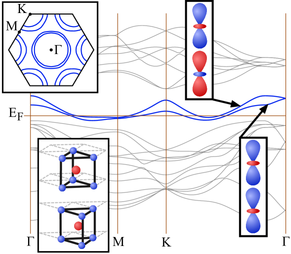
Niobium diselenide is a layered material, in which hexagonal layers of Niobium atoms are sandwiched between similar layers of Selenium atoms, displaced so that they lie above and below half of the Nb interstitial locations, as shown in the inset of Fig. 1. Consecutive sandwich layers are displaced to have the complementary half of the interstices occupied, giving two formula units per unit cell. The Fermi surface consists of two concentric barrel-shaped pockets centred around both the and the points, as well as a very small pancake-shaped pocket surrounding , which we ignore in the analysis below. The inner pockets at are seen in ARPES to develop the largest CDW gaps Borisenko et al. (2009); Rahn et al. (2012). The CDW itself is of the type, with three equivalent superposed modulations at with respect to one other.
To describe the electronic states, we employ a Slater-Koster tight-binding fit to the band structure using a basis of Se- and Nb- orbitals Slater and Koster (1954); Doran et al. (1978). For the two main bands crossing that give rise to the barrel-shaped pockets (which we will refer to as inner, developing the CDW instability, and outer), the fit is constrained by data from ARPES measurements Rahn et al. (2012), while the remaining bands are fit to recent LDA calculations Johannes et al. (2006). In agreement with earlier reports Doran et al. (1978), we find that both the inner and outer bands at are primarily composed of the orbitals centred on the two Nb atoms within a unit cell, in the form of bonding (inner) and anti-bonding (outer) combinations (as shown in Fig. 1).
Focussing on the two non-interacting bands at , we introduce the interaction between electrons and phonons :
| (1) |
where the bare phonon dispersion can be described by a Brillouin function tending to a maximum of at the zone boundary Weber et al. (2013). The electron-phonon coupling depends on the momenta, as well as the band indices and , of the the ingoing and outgoing electron states. Following Varma et al. we model both of these dependencies using knowledge purely of the electronic structure, which has been shown to work well for a range of transition metals and their compounds Varma et al. (1979). In terms of the matrices of tight-binding overlap integrals and generalized eigenvectors , the electron-phonon coupling matrix elements are given by Varma et al. (1979):
| (2) |
where a constant prefactor has been omitted, and the band velocity for electrons in band is defined in terms of the band energy as . In the interaction of equation (1) we restrict attention to the longitudinal component of , since only the longitudinal acoustic phonons are observed to soften in inelastic neutron and X-ray scattering experiments Weber et al. (2013).
Inserting the tight binding results into equation (2), we find that the inter-band electron-phonon coupling is strictly zero, while the intra-band coupling is about a factor of three stronger for the inner band than for the outer. This result immediately explains why the experimentally observed CDW gap is so much more pronounced in the inner band Borisenko et al. (2009); Rahn et al. (2012), since the static electronic susceptibility scales with the square of the electron-phonon coupling:
| (3) |
Here is the Fermi-Dirac distribution function, and the static Lindhard function is given by when . The absence of interband coupling causes the contributions of the two bands to the susceptibility to be entirely independent. This means that the lower value of the intra-band coupling in the outer band leads to an order of magnitude suppression of its contribution to , and therefore to a correspondingly reduced gap in its Fermi surface pocket. It is thus the orbital character of the electronic bands, and consequently the orbital dependence of the electron-phonon coupling, that causes a relative size difference between the CDW gaps in the pockets around the -point, even if they are equally well nested.
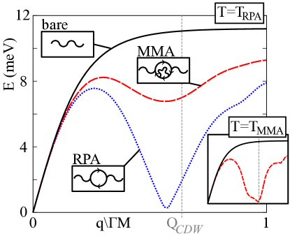
The expression for the susceptibility in equation (3) can further be used to quantify both the amount of nesting present in NbSe2, and to evaluate the relative contribution of the electron-phonon coupling matrix elements in selecting the observed value of the (incommensurate) ordering wave vector , with Wilson et al. (1974). In the left panel of Fig. 2, three susceptibilities are compared. The dotted blue line shows the susceptibility for a perfectly nested model with a single 1D band of cosine dispersion. The sharp peak characteristic of a nested Fermi surface is apparent. The dashed red line is the bare susceptibility in NbSe2, obtained by setting in equation (3). This does not include any of the momentum and orbital dependence of the electron-phonon coupling, and is the form that has been widely used in previous studies Soumyanarayanan et al. (2013); Johannes et al. (2006); Rahn et al. (2012). It is almost completely flat except for a very broad and low maximum far from , and can therefore not explain the observed ordering vector. The solid black line, on the other hand, displays the susceptibility of just the inner band. A broad but distinct maximum develops at the experimentally observed CDW vector. The selection of the ordering vector is thus shown to arise from the combined influence of both the electronic structure and the orbital and momentum dependent electron-phonon coupling, with neither contribution being negligible Borisenko et al. (2009); Rahn et al. (2012).
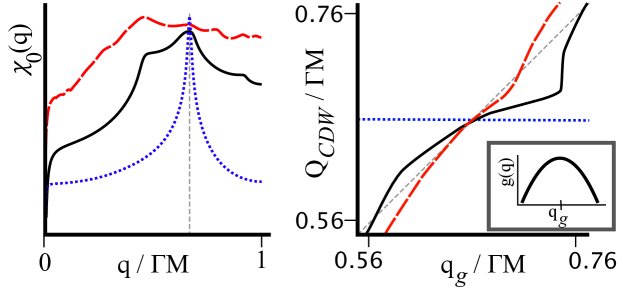
Restricting attention to the inner band, we can quantify the extent to which nesting contributes to the selection of . For this purpose we temporarily switch to a simplified form of , which is a function only of the momentum transfer: . Even though in general the shape of the susceptibility is determined by both the incoming momentum and the momentum transfer, modelling the electron-phonon coupling in this simplified form allows us to directly quantify the effect of varying the position of its peak, and thus its influence on the position of the peak in . The values of the parameters , , and can be estimated by fitting the experimentally observed phonon softening Weber et al. (2011) to the expression for the renormalized phonon energy in the Random Phase Approximation (RPA), , where we take to be the high temperature (unrenormalized) dispersion. In the right panel of Fig. 2 we plot the variation of the maximum in the susceptibility (i.e. the expected ) as is varied along ). Again, the blue dotted line represents the situation of a perfectly nested band structure, in which the electron-phonon coupling never overcomes the peak in the susceptibility, and thus has no effect on . The red dashed line has the same form of for all bands, and is close to a straight line at (grey dashed line). A true line would indicate that , implying that the CDW vector is completely determined by the electron-phonon coupling, with the electronic structure having no influence at all. The solid black line, which shows the behaviour of just the inner band, interpolates between these two extremes. There is no plateau, but there is an indication of some flattening, suggesting that while it is mainly the momentum dependence of the electron-phonon coupling which determines the value of CDW ordering vector, the rôle of the electronic structure cannot be neglected entirely.
The CDW Gap
Having identified the importance of both electron-phonon coupling and electronic structure, we now revert to using the full expression of equation (2). To compare the size and shape of the CDW gap resulting from the orbital and momentum dependent to the experimentally observed behaviour, the RPA gap equations shown diagrammatically in Fig. 3 are solved self-consistently. We simplify the calculation by using the gap matrix which includes all higher harmonics appropriate for a commensurate CDW wave vector at , as an approximation for the gap matrix of the incommensurate CDW in NbSe2 with . We further fix the values of the electronic self-energies, and constrain the momentum dependence of the gap function to a five parameter tight-binding fit consistent with the symmetries of the lattice. A self-consistent solution for the gap function to all orders in RPA can then be found by searching for a fixed point in the flow of consecutive iterations of the gap equation.
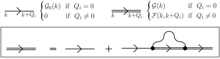
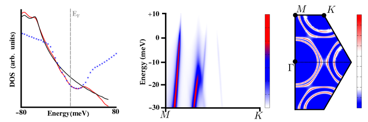
Fig. 4 shows energy and momentum cuts through the electronic spectral functions resulting from the solution to the gap equations, as well as their corresponding DOS. A good match with the shape of the experimentally determined DOS in STS experiments can be achieved by introducing a meV shift in the chemical potential, which falls well within the range of experimental uncertainty Soumyanarayanan et al. (2013). The overall strength of the electron-phonon coupling, the only free parameter in the theory, is set to give a maximum CDW gap magnitude of meV. The Fermi surface on the right of Fig. 4 then shows a CDW gap opening on the inner band only, and Fermi arcs forming at the same locations as observed in ARPES measurements Borisenko et al. (2009); Rahn et al. (2012); Chatterjee et al. (2015). The extent of the gap on the Fermi surface, its size (apparent from the dispersion’s back-folding in the centre of Fig. 4), and its restriction to one band, are all in agreement with experimental findings Borisenko et al. (2009); Rahn et al. (2012); Chatterjee et al. (2015). The plot of the DOS on the left indicates that these results, which were previously interpreted to imply a gap size of meV Borisenko et al. (2009); Rahn et al. (2012), are in fact consistent with the STS results indicating a particle-hole asymmetric gap of meV Soumyanarayanan et al. (2013); Chatterjee et al. (2015). The asymmetry hides most of the gap structure above , where photoemission intensity is suppressed by the Fermi-Dirac distribution Chatterjee et al. (2015). The comparison between the experimental STS data and the calculated RPA results shows that the particle-hole asymmetry arises naturally from the interplay between the electronic structure and the momentum-dependent electron-phonon coupling.
The Pseudogap
The central rôle of the orbital and momentum dependent electron-phonon coupling in determining both the CDW propagation vector and the structure of the gap, suggests that the charge order in NbSe2 falls in the strong-coupling regime, in which the electronic structure alone is not sufficient to characterize the emergent charge order. In the presence of strong electron-phonon coupling, it is well-known that the entropy associated with localized lattice vibrations plays an essential part in the system’s thermal evolution McMillan (1975). To understand the properties of NbSe2 above its CDW transition temperature, it is therefore necessary to consider the influence of phonon fluctuations beyond RPA. The so-called Mode-Mode coupling Approximation (MMA) includes the lowest order terms of this type, and has been shown to successfully describe the influence of phonon fluctuations in some of the electronic properties of related dichalcogenide materials like TaSe2 and TiSe2 Inglesfield (1980); Yoshiyama et al. (1986). The additional terms included in the MMA fall into two categories: a vertex correction, which we neglect by appeal to Migdal’s theorem because of the large momentum transfer associated with , and self-energy corrections to the internal electron lines (indicated diagrammatically in Fig. 5), which we include. In agreement with recent X-ray scattering observations on NbSe2 Weber et al. (2011, 2013), the MMA-renormalized phonon spectrum shown in the inset of Fig. 5 shows a broad range of phonon modes softening near the transition temperature, rather than the sharp Kohn anomaly indicative of well-nested materials. The momentum of the softest phonon mode at the transition temperature coincides with the experimentally observed CDW propagation vector.
The softening of phonon modes, as the charge-ordered state is approached from high temperatures, is suppressed by the fluctuations beyond RPA. Since the temperature at which the first phonon mode reaches zero energy defines the transition temperature , this means that the charge ordering transition temperature in MMA, , is suppressed with respect to the corresponding value in RPA, . Choosing the overall strength of the electron-phonon coupling such that matches the experimentally observed value of , Fig. 5 shows that the corresponding RPA transition occurs already at . Physically, this suppression of the transition temperature can be ascribed to the presence of fluctuations in the phonon field. In the temperature range , the phonon fluctuations are strong enough to destroy the long range order predicted by (mean field) RPA theory. In that regime, the amplitude of the static order parameter vanishes, , but dynamic fluctuations of the order parameter persist, Yoshiyama et al. (1986); McMillan (1975). The result is a locally-fluctuating short-range ordered state, characterized by the presence of a non-zero order parameter amplitude, without any long-range phase coherence Chatterjee et al. (2015). Due to the non-zero amplitude, the gap in the electronic structure will survive even above the transition temperature , in the form of a pseudogap phase Borisenko et al. (2009); Chatterjee et al. (2015). The dynamical fluctuations in this regime may become locally pinned in the presence of defects, creating islands of order up to , in agreement with recent STM and X-ray scattering experiments Chatterjee et al. (2015); Arguello et al. (2014). The properties of this regime are reminiscent of the features which characterize the pseudogap phase of cuprate high-temperature superconductors Timusk and Statt (1999), which have recently been shown typically to contain charge-ordered phases of their own Chang et al. (2012); Ghiringhelli et al. (2012). Specific similarities are the presence of a pseudogap, Fermi surface arcs, dynamical fluctuations and a corresponding sensitivity to the timescales employed by experimental probes, as well as the existence of the crossover to the normal state at . Note that the existence of a crossover temperature , between the pseudogap and disordered regimes predicted here, falls outside of the temperature range that has been probed in NbSe2 to date Borisenko et al. (2009); Arguello et al. (2014).
Discussion
Although various theories for the formation of charge order in NbSe2 have been able to explain many parts of its diverse experimental signatures, the material has so far evaded the simultaneous description of all of its properties by a single consistent theoretical account. The main features which remain difficult to reconcile with the weak-coupling theories considered so far, include the emergence of CDW order in spite of a lack of nesting in the electronic structure, and an anomalously flat electronic susceptibility, the softening of a broad range of phonon modes rather than a sharp Kohn anomaly, a discrepancy in the sizes of the CDW gap observed in different electron pockets in spite of them being similarly nested, disagreement about the existence, size and particle-hole symmetry of the CDW gap as seen by different experimental probes, and the presence of a pseudogap phase characterized by locally fluctuating charge order above the CDW transition temperature. We have shown here that all of these observations can be understood to result from the presence of a strong orbital and momentum dependent electron-phonon coupling.
The combination of both the momentum-dependent coupling and the particular electronic structure of NbSe2 is found to be crucial in the selection of the charge ordering vector, while the orbital dependence naturally explains the different behaviours of different Fermi surface pockets. The same dependencies on momentum and orbital character are also reflected in the emergence of a particle-hole asymmetric gap, which has a size of about meV, centred above where it is largely inaccessible to observation by ARPES. These observations put NbSe2 in the regime of strongly-coupled charge-ordered materials, in the sense that the specifics of the electron-phonon coupling qualitatively affect the properties of the ordered state.
The pseudogap phase above may arise in such a scenario from local fluctuations of the lattice, which destroy the long-range phase coherence of the CDW order parameter but not its amplitude. Taking into account higher order phonon fluctuations, we find that indeed the mean-field transition temperature is suppressed, leading to a regime above characterized by the absence of long-range charge order but the presence of phonon fluctuations. This agrees with the experimental observation of Fermi arcs and a pseudogap above the transition temperature, as well as that of pinned charge order at high temperatures around local defects. All of these signatures of the pseudogap phase are reminiscent of similar features seen in the pseudogap phase of cuprate high-temperature superconductors.
In conclusion, while the Peierls mechanism can explain charge ordering in 1D systems entirely in terms of the electronic structure, this is not the natural starting point for higher-dimensional materials. Instead, it is necessary to include full information about the dependence of the electron-phonon coupling on the momenta and orbital characters of the electronic states involved in the CDW formation. This is evidenced by the present case of NbSe2, a typical quasi-2D material without a strongly nested Fermi surface, in which knowledge about all aspects of the electron-phonon coupling prove to be essential in explaining the full range of experimental observations. We suggest this consideration to be generically applicable across charge-ordered quasi-2D and quasi-3D materials lacking strong nesting features. In particular, the full momentum and orbital dependence of the electron-phonon coupling should be taken into account throughout the class of transition metal dichalcogenides and related material classes, including high-temperature superconductors.
Acknowledgments
The authors thank M. R. Norman for suggesting the approach discussed here, and for numerous insightful discussions.
References
- Wilson et al. (1974) J. A. Wilson, F. J. Di Salvo, and S. Mahajan, Phys. Rev. Lett. 32, 882 (1974).
- Peierls (1991) R. Peierls, More Surprises in Theoretical Physics (Princeton Series in Physics, 1991).
- Doran (1978) N. J. Doran, J. Phys. C: Solid State Phys. 11 (1978).
- Borisenko et al. (2009) S. V. Borisenko, A. A. Kordyuk, V. B. Zabolotnyy, D. S. Inosov, D. Evtushinsky, B. Büchner, A. N. Yaresko, A. Varykhalov, R. Follath, W. Eberhardt, L. Patthey, and H. Berger, Phys. Rev. Lett. 102, 166402 (2009).
- Johannes et al. (2006) M. D. Johannes, I. I. Mazin, and C. A. Howells, Phys. Rev. B 73, 205102 (2006).
- Rice and Scott (1975) T. M. Rice and G. K. Scott, Phys. Rev. Lett. 35, 120 (1975).
- Weber et al. (2011) F. Weber, S. Rosenkranz, J.-P. Castellan, R. Osborn, R. Hott, R. Heid, K.-P. Bohnen, T. Egami, A. H. Said, and D. Reznik, Phys. Rev. Lett. 107, 107403 (2011).
- Hess et al. (1991) H. Hess, R. Robinson, and J. Waszczak, Physica B: Condensed Matter 169, 422 (1991).
- Wang et al. (1990) C. Wang, B. Giambattista, C. G. Slough, R. V. Coleman, and M. A. Subramanian, Phys. Rev. B 42, 8890 (1990).
- Rahn et al. (2012) D. J. Rahn, S. Hellmann, M. Kalläne, C. Sohrt, T. K. Kim, L. Kipp, and K. Rossnagel, Phys. Rev. B 85, 224532 (2012).
- Straub et al. (1999) T. Straub, T. Finteis, R. Claessen, P. Steiner, S. Hüfner, P. Blaha, C. S. Oglesby, and E. Bucher, Phys. Rev. Lett. 82, 4504 (1999).
- Harper et al. (1975) J. Harper, T. Geballe, and F. D. Salvo, Phys. Lett. A 54, 27 (1975).
- Varma and Simons (1983) C. M. Varma and A. L. Simons, Phys. Rev. Lett. 51, 138 (1983).
- Moncton et al. (1975) D. E. Moncton, J. D. Axe, and F. J. DiSalvo, Phys. Rev. Lett. 34, 734 (1975).
- Soumyanarayanan et al. (2013) A. Soumyanarayanan, M. M. Yee, Y. He, J. van Wezel, D. J. Rahn, K. Rossnagel, E. W. Hudson, M. R. Norman, and J. E. Hoffman, Proceedings of the National Academy of Sciences 110, 1623 (2013), http://www.pnas.org/content/110/5/1623.full.pdf+html .
- Rainer and Sauls (1992) D. Rainer and J. A. Sauls, “Strong-coupling theory of superconductivity,” in Superconductivity: From Basic Physics to the Latest Developments (1992) Chap. 2, pp. 45–78.
- Wang et al. (2007) Y. Wang, J. Yan, L. Shan, H.-H. Wen, Y. Tanabe, T. Adachi, and Y. Koike, Phys. Rev. B 76, 064512 (2007).
- Hashimoto et al. (2014) M. Hashimoto, I. M. Vishik, R.-H. He, T. P. Devereaux, and Z.-X. Shen, Nature Physics 10, 483 (2014).
- Weber et al. (2013) F. Weber, R. Hott, R. Heid, K.-P. Bohnen, S. Rosenkranz, J.-P. Castellan, R. Osborn, A. H. Said, B. M. Leu, and D. Reznik, Phys. Rev. B 87, 245111 (2013).
- Grüner (1988) G. Grüner, Rev. Mod. Phys. 60, 1129 (1988).
- McMillan (1975) W. L. McMillan, Phys. Rev. B 12, 1187 (1975).
- Yoshiyama et al. (1986) H. Yoshiyama, Y. Takaoka, N. Suzuki, and K. Motizuki, J. Phys. C: Solid State Phys. 19, 5591 (1986).
- Chatterjee et al. (2015) U. Chatterjee, J. Zhao, M. Iavarone, R. D. Capua, J. P. Castellan, G. Karapetrov, C. D. Malliakas, M. Kanatzidis, H. Claus, J. P. C. Ruff, F. Weber, J. van Wezel, J. C. Campuzano, R. Osborn, M. Randeria, N. Trivedi, M. R. Norman, and S. Rosenkranz, Nat. Commun. 6, 6313 (2015).
- Arguello et al. (2014) C. J. Arguello, S. P. Chockalingam, E. P. Rosenthal, L. Zhao, C. Gutiérrez, J. H. Kang, W. C. Chung, R. M. Fernandes, S. Jia, A. J. Millis, R. J. Cava, and A. N. Pasupathy, Phys. Rev. B 89, 235115 (2014).
- Emery et al. (1999) V. J. Emery, S. A. Kivelson, and J. M. Tranquada, Proc Natl Acad Sci U S A. 96, 8814 (1999).
- Walstedt et al. (2011) R. E. Walstedt, T. E. Mason, G. Aeppli, S. M. Hayden, and H. A. Mook, Phys. Rev. B 84, 024530 (2011).
- Chang et al. (2012) J. Chang, E. Blackburn, A. T. Holmes, B. C. N, J. Larsen, J. Mesot, R. Liang, D. A. Bonn, W. N. Hardy, A. Watenphul, M. v. Zimmermann, E. M. Forgan, and S. M. Hayden, Nature Physics 8, 871 (2012).
- Ghiringhelli et al. (2012) G. Ghiringhelli, M. L. Tacon, M. Minola, S. Blanco-Canosa, C. Mazzoli, N. B. Brookes, G. M. D. Luca, A. Frano, D. G. Hawthorn, F. He, T. Loew, M. M. Sala, D. C. Peets, M. Salluzzo, E. Schierle, R. Sutarto, G. A. Sawatzky, E. Weschke, B. Keimer, and L. Braicovich, Science 337, 821 (2012).
- Slater and Koster (1954) J. C. Slater and G. F. Koster, Phys. Rev. 94, 1498 (1954).
- Doran et al. (1978) N. J. Doran, D. J. Titterington, B. Ricco, and G. Wexler, J. Phys. C: Solid State Phys. 11, 685 (1978).
- Varma et al. (1979) C. M. Varma, E. I. Blount, P. Vashishta, and W. Weber, Phys. Rev. B 19, 6130 (1979).
- Inglesfield (1980) J. E. Inglesfield, Journal of Physics C: Solid State Physics 13, 17 (1980).
- Timusk and Statt (1999) T. Timusk and B. Statt, Reports on Progress in Physics 62, 61 (1999).