Frequency dispersion of nonlinear response of thin superconducting films in Berezinskii-Kosterlitz-Thouless state.
Abstract
The effects of microwave radiation on transport properties of atomically thin films were studied in the 0.1-13 GHz frequency range. Resistance changes induced by microwaves were investigated at different temperatures near the superconducting transition. The nonlinear response decreases by several orders of magnitude within a few GHz of a cutoff frequency . Numerical simulations that assume response to follow the - characteristics of the films reproduce well the low frequency behavior, but fail above . The results indicate that 2D superconductivity is resilient to high-frequency microwave radiation, because vortex-antivortex dissociation is dramatically suppressed in 2D superconducting condensate oscillating at high frequencies.
pacs:
72.20.My, 73.43.Qt, 73.50.Jt, 73.63.HsTransport properties of thin superconducting films have attracted much interest due to a fascinating physical phenomenon, the Berezinskii-Kosterlitz-Thouless (BKT) transition, predicted to occur at the critical temperature lower than the temperature of the superconducting transition in bulk samples berezinskii1972 ; kosterlitz1973 ; kosterlitz1978 ; jose2013 . The BKT phase transition originates from long-range (logarithmic) interactions between vortex excitations in a two-dimensional (2D) superconducting condensate. Below , the dominant thermal excitations are vortex-antivortex (V-AV) pairs. A superconducting current does not move pairs, thus producing no energy dissipation. However, the current can break some of V-AV pairs, generate free vortices, set them in motion via the Lorentz force, and thus make the transport dissipative halperinnelson1979 ; huberman1978 ; ambegaokar1980 . The induced dissociation of V-AV pairs depends on the current strength and thus results in an extraordinary violation of the Ohm’s law. With this motivation, the strong nonlinear response to the electric current in thin superconducting films was investigated extensively epstein1981 ; kadinepsteingoldman1983 ; fioryhebardglaberson1983 ; goldman2013 . Despite significant progress, important many-body and edge effects in the V-AV pair dissociation are still under debate gurevich2008 ; kogan2007 . Note that the majority of studies of the nonlinear transport in the BKT regime have in fact been done in the domain. How condensate oscillations affect the V-AV dissociation is still unclear. Finally, due to strong phase fluctuations the BKT phenomena are significantly enhanced in superconducting cuprates, especially in heterostructures with a few superconducting copper oxide layers lemberger2007 . Our recent studies of nonlinearities in MBE-grown heterostructures show that the vortex nonlinearity in the low resistive state exceeds the heating nonlinearity by up to four orders in magnitude bo2013 .
Here, we present experimental investigations of nonlinear transport properties of atomically thin films, over a broad frequency range from to 13 GHz. The experiments indicate a dramatic decrease of the nonlinear response at high drive frequencies, suggesting significant reduction of the V-AV pair dissociation in the oscillating superconducting condensate.
The experiments were performed on thin (LSCO) films synthesized by Atomic-Layer-by-Layer Molecular Beam Epitaxy, providing precise atomically thin layers gozar2008 ; logvenov2009 ; bollinger2011 . On the extreme level of control, delta-doping in a single layer has been demonstrated logvenov2009 . Recently a linear response of such films in the BKT state has been studied gasparov2012 ; bilbro2011 . Present samples have three distinct layers. The top and the bottom layers, each 5 unit cells (UC) thick, are made of strongly overdoped (0.41) normal metals. The sample A, with 5 UC thick inner layer of , shows the BKT transition at 7K dietrich2014 . The sample B with 1.5 UC thick inner layer of has 5K. Below we study nonlinear response of the BKT state at .
The films were patterned into the shape of Hall-bar devices with the width 200 m and the distance between the voltage contacts 800 m. A direct current was applied through a pair of current contacts, and the longitudinal voltage was measured between the potential contacts. The sample and a calibrated thermometer were mounted on a cold copper finger in vacuum. The electromagnetic (EM) radiation was guided by a rigid coaxial line and applied to samples as shown in the upper insert in Fig. 1. A 50 resistor terminates the end of the coax and provides the broadband matching of the EM circuit. The EM power and amplitude of the microwave voltage at the end of the coax were measured in-situ using the non-selective bolometric response of the 50 resistor dietrich2014 . In what follows, the measured nonlinear response is normalized with respect to the calibrated EM power , which takes into account all the effects of EM transmission (reflection) to (from) the sample stage.
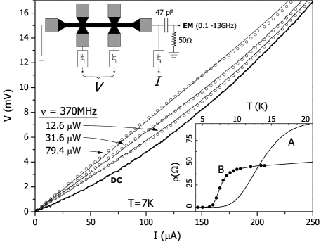
Fig. 1 shows the dependence of the voltage on the current taken at different powers of a low frequency radiation. The thick solid line presents the - dependence with no radiation applied. The EM radiation increases the resistance as shown by thin solid lines. To evaluate numerically the radiation effect the electrical connection (coupling) between the coax and the sample was approximated by a high-frequency contact resistance , which determines the total voltage and current applied to the sample, assuming that the electromagnetic response follows the nonlinear - dependence dietrich2014 . The time averaged and are denoted by the open circles in Fig. 1. The resistance was used as the single fitting parameter for each computed curve, providing a good agreement between the low frequency experiments and the simulations.
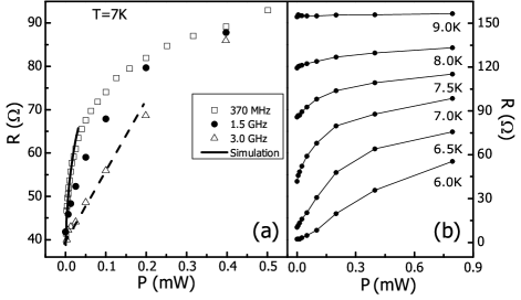
At small currents, both the experiment and the simulations display a linear relation between the current and voltage - Ohm’s Law. Fig. 2b presents the dependence of the ohmic resistance on microwave (MW) power ( 1.5 GHz) taken at different temperatures. The filled dots are the slopes of the - dependencies at small currents. The power dependence varies considerably with the temperature. Close to the superconducting state the microwave-induced resistance variations are strong, whereas near the normal state the variations are weak. The shape of the dependence changes with the temperature. In particular, at = 6 K the dependence looks more linear than at = 6.5 K.
Significant changes of the power dependence are found in the response to microwaves with different frequencies. Fig. 2a shows the power dependencies of the resistance obtained at frequencies = 0.37, 1.5, and 3 GHz. At low frequency = 0.37 GHz, the dependence is in a good agreement with the numerical simulation. At high frequencies, the nonlinear response is much weaker and has a different functional form. To highlight the difference, the values of MW power at frequency 3 GHz were scaled down by a factor of 2. A comparison of power dependencies indicates that at a low power the nonlinear response is considerably weaker at a high frequency (3 GHz) than at a low frequency (0.37 GHz). At a high power the strength of the high frequency nonlinearity is restored.
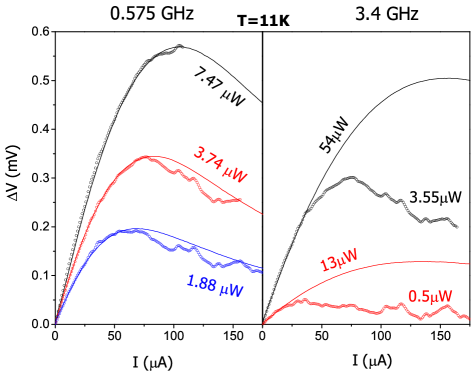
Fig. 3 shows the dependence of radiation-induced variations of the voltage on bias taken at different frequencies and power levels, as labeled. At small currents, the response is linear, indicating no observable rectification in the device. The left panel demonstrates the effect of the low-frequency radiation ( = 0.575 GHz) on the resistance. All three curves are in very good agreement with the ones obtained by numerical simulations for the same radiation powers dietrich2014 . The simulations replicate all the details of the experiments including the shift of the observed maximum with increased power using single fitting parameter . The right panel shows the effect of the high frequency ( = 3.4 GHz) radiation. One can see that the high-frequency response does not follow the - curve and cannot be explained by a reduction (re-scaling) of the MW current.
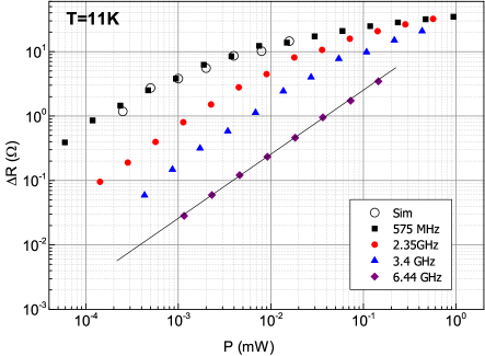
At small currents, the linear part of the voltage variations is related to the change of the ohmic resistance: . Figure 4 displays the behavior of the resistance variation with the power at different frequencies. At a small power, the induced resistance variations are proportional to the power. At higher powers, the dependence is weaker. At higher frequencies, the transition to weak power dependence occurs at a higher power. At the highest power levels all dependencies converge (see Fig. 2a).
An analysis indicates several distinct features of the nonlinear response presented in Fig. 1. At small currents the - dependence is well approximated by a combination of linear and cubic terms bo2013 . The dependence is presented below:
| (1) |
where is the Ohmic resistance, the coefficient is a constant. The high-current behavior is in agreement with the one expected within the BKT scenario: halperinnelson1979 ; kadinepsteingoldman1983 ; fioryhebardglaberson1983 . The exponent decreases from 8 to 1 as the temperature increases, indicating a BKT transition at dietrich2014 . In accordance with Eq.(1) at small currents , the voltage variations are proportional to the bias , which agrees with Fig. 3, and proportional to the RF power , which agrees with Fig. 4. The decrease of the nonlinear response shown in Fig. 3 at high biases and the transition to a weaker power dependence presented in Fig. 4 are the results of the high current response at 2.
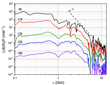
Fig. 5 presents the frequency dependence of the nonlinear response, taken at different temperatures and small powers . At low temperatures, 9 K 11 K, the response decreases by 3-4 orders in magnitude, as the frequency increases above few GHz. This is in a good agreement with the reduction of the nonlinearity by 3-4 order of magnitude observed between the regimes of V-AV depairing at 10 K and electron heating in the normal state (see Fig. 3b in bo2013 ).
To be sure that the observed effect is not related to a strong decrease in the microwave coupling, we have evaluated the MW current through samples by investigating the MW reflection in the same setup dietrich2014 . These studies indicate some frequency dispersion in the MW current. However, the dispersion is nearly uniform and significantly smaller (a variation by a factor of 3-4) than the observed reduction of the nonlinear response by 3-4 orders of magnitude. Independent measurements of MW voltage, current, and the nonlinear response in several samples allow us to conclude that the observed reduction of the nonlinearity is of fundamental nature.
Since the reduction is strong, we associate it with the frequency suppression of the dominant mechanism in BKT regime - the current induced V-AV pair dissociation. If in the course of high-frequency oscillation the distance between the vortex and antivortex within a pair does not exceed a critical distance , then the pair can survive. At higher power, the amplitude of V-AV oscillations may exceed the critical distance , making the response similar to the one obtained at low frequency. It corresponds to Fig. 2a and Fig. 4.
An analysis of the oscillating vortex motion inside a V-AV pair in the presence of depairing current shows rich physics, analogous to the Kapitza pendulum with a vibrating pivot point landau1976 . Position of a vortex with the mass moving in a medium with the viscosity under effect of a time-dependent external potential is given by
| (2) |
The potential is a sum of V-AV interaction and a potential of Lorentz force ambegaokar1980 : , where is a size of the vortex core and , where and are density and the mass of superconducting carriers. We express the supercurrent density as a sum of the bias and current oscillations at angular frequency . An analysis of vortex motion for critical pairs near the saddle point of the potential () shows a reduction of the vortex displacement at high frequencies: . Moreover, at , the depairing is strongly suppressed due to the phase shift between the vortex displacement and the barrier height. At the moments when the potential reaches a minimum, the displacement is the smallest, thus preventing the V-AV dissociation. Finally at high frequencies a nonlinear analysis landau1976 of Eq.(2) indicates an effective attractive force inside the pair, which is proportional to the square of the vortex displacements: . These effects reduce the pair dissociation at high driving frequencies. Although the origin of the cutoff frequency requires further research, we note that an evaluation of the frequency is in a good agreement with our data. Using the Stephen-Bardeen viscosity stephen_bardeen1965 and considering the vortex mass as a total mass of electrons in the core volovik1997 we get the characteristic frequency of = 2 GHz at the core radius of 8 nm, which is approximately two times bigger than the superconducting coherence length . The above analysis points toward the crucial importance of the displacement-force phase relations in the nonlinear response of the bulk BKT state supporting substantially the fundamental origin of the observed phenomenon.
In summary, strong nonlinear response to low frequency radiation is observed in atomically thin superconducting films, in BKT state. The response decreases by several decades within a few GHz above the cutoff frequency 2 GHz. This indicates that 2D superconductivity is quite resilent to the high frequency radiation because of a strong reduction of the vortex-antivortex dissociation in oscillating 2D superconducting systems. This general conclusion is in agreement with the results of the linear response studies of the BKT state in thin disordered films of traditional superconductors. In particular, detailed investigations of the conductivity in the range 9-120 GHz show only frequency-dependent Drude absorption without any measurable dissipation due to vortex-antivortex dissociation crane2007 .
Sample synthesis by ALL-MBE and characterization (I.B.) and device fabrication (A.T.B.) were supported by U.S. Department of Energy, Basic Energy Sciences, Materials Sciences and Engineering Division. Work at CCNY and SUNY was supported by National Science Foundation, Division of Electrical, Communications and Cyber Systems (ECCS 1128459).
I Supplemental Material.
II Transport in DC Domain. BKT transition.
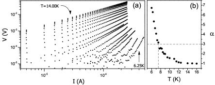
According to the BKT theory, - characteristics should display a dependence where the temperature-dependent exponent, , ranges from one in the normal state and increases as temperure decreases, passing through it’s critical value at the Brezenskii–Kosterlitz–Thouless (BKT) transition temperature, halperinnelson1979 ; kadinepsteingoldman1983 ; fioryhebardglaberson1983 . Figure 6a presents - dependencies of Sample A plotted in log-log scales. The dependencies obtained at different temperatures in a range from 6.25-14.00 Kelvin at zero magnetic field. At high applied currents the dependencies are in agreement with the power law , where coefficient depends on temperature.
Fitting these curves to the power-law - function yields the temperature dependence of . Figure 6b presents the results of the fitting. The coefficient varies from about 7 at 6.25K to 1 at at 12K indicating a BKT transition at 7.5 K corresponding to . We note that in accordandce with the thermal conductance per unit area of the sample W/Kcm2 bo2013 the electron overheating at temperatures =7-10K near the BKT transition is below 0.1 K at the highest currents applied to the sample. Thus contributions of thermal effects to the observed nonlinearity are negligibly small.
III Numerical Simulations and Bolometric Calibration.
The goal of the simulation is to use I-V characteristic of the sample to reproduce the I-V characteristics under the MW excitation. Figure 7 presents the approximation of the microwave circuit used in experiments. The circuit contains a 50 Ohms terminal resistance which provides a broadband coupling of the circuit with microwaves. The nonlinear resistance describes the sample response. The contact resistance couples microwaves with the sample.To isolate the and the microwave circuits a 47 pF capacitor is added in series with the sample. The AC resistance of the capacitor is included in the .
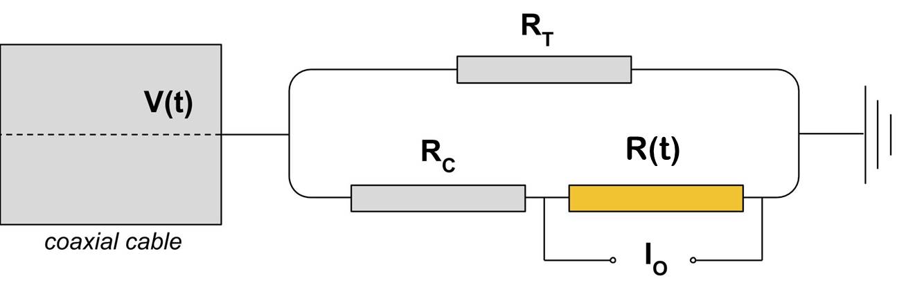
The simulation is based on the assumption that the nonlinear response to EM radiation follows the I-V characteristics. The response of the circuit is described by the following set of equations:
| (3a) | |||
| (3b) | |||
| (3c) | |||
Eq.(3a) describes voltage in the microwave (AC) circuit. The AC voltage at the end of the coax is the sum of the voltage applied to the contact resistance and the AC voltage applied to the sample , where is the AC current through the sample and the resistance . Eq.(3b) describe the total current through the sample, which is sum of AC () and () currents. The third equation relates the voltage applied to the sample to the total current, using the V-I characteristic obtained in the experiment.
The equations yield AC current and voltage at given microwave voltage , contact resistance and current . The time average of the AC response yields contributions to current and voltage and makes a V-I dependence in the presence of the microwave radiation. The V-I characteristic depends on the contact resistance . A comparison between simulated and the actual V-I characteristics yields the contact resistance at given MW voltage (power ). The tables below give the fitting parameter at different powers .
| Figure 1. |
|
||||||||||||||||||
|---|---|---|---|---|---|---|---|---|---|---|---|---|---|---|---|---|---|---|---|
| Figure 2. |
|
||||||||||||||||||
| Figure 3. |
|
We note that for all Figures except Fig.3 , where is a calibrated power at the end of the coaxial line.
Fig. 3 shows a reduction of the upper limit of the bias for the simulations at high MW powers. This is related to the limited range of currents in the experimental V-I dependences used for the numerical simulation: . In accordance with Eqs.(3b,c)the simulation calculates the voltage using the V-I dependence . To obtain the voltage V the value must be less . In Fig.3 it reduces progressively the range of the biases at which the simulation works at higher MW currents (powers).
III.1 Bolometric calibration of MW power.
The in-situ bolometric calibration of the microwave power applied to the end of the coax is based on the following measurement. In experiment the resistor terminating the coaxial line (see Fig.7) is thermally anchored to a copper sample holder. A microwave power , applied to the end of the coax, heats the resistor . It decreases the amount of the electric power, , supplied by a temperature control unit to heater, which is attached to the sample holder to maintain the sample temperature. The change of the heating power is found by measuring voltage applied to the heater (resistance =100 ) with and without MW radiation. The bolometric calibration of the MW power is based on the conservation of the total energy supplied to the stage: .
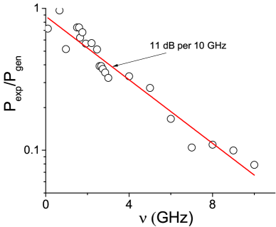
Fig.8 shows the ratio of the calibrated power to the power at the output of the MW generator at different frequencies. The calibrated power decreases by about 10 times at high frequencies. The power decrease is found to be in agreement (within 40% deviations) with total microwave losses in coaxial lines between the MW generator and the sample, which were measured separately in transmission and reflection experiments. This agreement verifies the expected independence of the power losses in the terminal resistance on the frequency.
The bolometric calibration is done in the presence of the superconducting samples. The fact that the decrease in supplied MW power is largely due to MW losses in transmission lines indicates also a relatively weak effect of the superconducting samples attached to the end of the coaxial line on the overall microwave reflection from the sample stage. It is in accord with measurements of the reflection coefficient from the sample stage presented in the next section. The bolometric calibration allows computing the microwave voltage at the end of the coax: . The voltage is used in the numerical simulations.
IV Microwave Coupling to the Samples: Reflection Measurements.
In the low frequency domain the nonlinear behavior (and the contact resistance ) is found to be nearly frequency independent taking into account the bolometric calibration of the power applied to the end of the coaxial line. At high frequencies the response does not follow the curves and the extraction of the contact resistance from the comparison with the numerical simulations is not possible. To evaluate the coupling of the EM radiation to the sample at high frequencies broad band measurements of a reflected microwave power were performed at two temperatures and corresponding to normal and superconducting states of the samples. Since in the normal state the superconductivity is absent the difference between two reflected signals indicate the strength of the coupling of the MW radiation to the superconducting condensate at different frequencies. The microwave broad band measurements (1 to 7 GHz) demonstrate that microwaves are quite uniformly coupled to the superconducting condensate in the studied frequency range indicating that frequency variations of the contact resistance are not significant for the observed strong reduction of the nonlinear response at high drive frequencies. Details of these experiments are presented below.
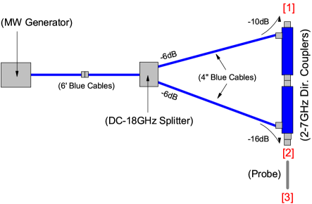
The setup of the reflection experiments is shown in Fig.9. The microwave power supplied by a microwave generator splits between two channels. The reference (upper) channel provides a reference signal supplied through a broad band directional coupler (-10dB) to a broad band microwave detector, which is attached to port [1]. The sample (lower) channel supplies microwave radiation to another directional coupler (-16dB), which directs the radiation to the sample attached to port [3] of a semi-rigid coaxial line (probe) connected to the port [2] of the coupler. Reflected from the sample signal is guided by the same coax back to the detector, where it interferes with the reference signal . Due to a significant difference in lengths of the reference and sample channels variations of the microwave wavelength (frequency) yield oscillating interference signal on the detector. At a small microwave amplitude the detected signal is proportional to microwave power , in other words, to the square of the microwave voltage:
| (4a) | ||||
| (4b) | ||||
| (4c) | ||||
where these and are the reference and reflected voltages, considered on the phasor diagram and is the phase difference between and signals. In the last equation the reflected signal was substituted with the incident voltage at port [2], using the reflection coefficient at the bottom of the probe (port [3]) and the microwave losses in the coaxial line between ports [2] and [3].
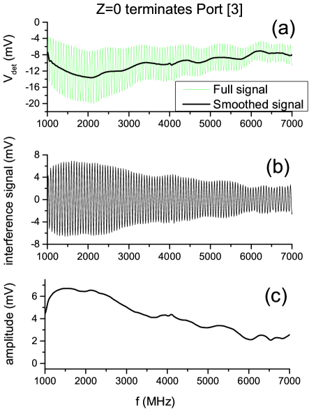
Terminating the port [3] by zero resistance (terminal impedance Z=0) one can measure the interference pattern corresponding to the complete reflection of microwaves from the port [3]. Figure 10(a) presents the detector signal corresponding to the complete microwave reflection (Z=0) as function of microwave frequency. Fast oscillations corresponds to the interference between and , while the slow variations of the signal corresponds mostly to variations of the reference signal . Contributions of the reflected signal to the microwave background are less than 10% and are neglected below. To separate the interference term (fast oscillations) from the background a FFT filter was applied resulting in the thick curve presented in Fig.10(a). A subtraction of the background from the detector response yields the interference term shown in Fig.10(b). In the case of the complete reflection the reflection coefficient . The corresponding amplitude of the interference term is shown in Fig.10(c). A decrease of the interference amplitude below 2 GHz is related to the decrease of and due to a properties of the couplers, which are designed to work in the range between 2 and 7 GHz. Decrease of the amplitude at high frequencies is related to microwave losses in the coaxial cable ().
When a sample attached to the port [3] the amplitude of the interference term is , where is the coefficient describing the microwave reflection from the sample. One can see that the ratio between this interference term and the amplitude of the interference term corresponding to Z=0 yields the normalized interference term , which is proportional to the magnitude of the reflection coefficient from the sample. The phase contains a contribution related to the phase of the reflection coefficient. Thus the product contains both the amplitude and the phase of the reflection coefficient. Below we will name the product as reflection coefficient. Fig. 11(a) presents the reflection coefficient of Sample C as a function of the frequency. Sample C has the same structure as Sample B.
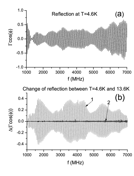
The reflection coefficient depends on the impedance of the microwave circuit containing the sample. A low frequency approximation of the microwave circuit is shown in Fig.7. The impedance depends on contributions from the 50 Ohm terminal resistor , contact resistance and the sample. At high frequencies the impedance may contains contributions related to a geometry of the sample holder, in particular, to finite lengths of the MW feeding leads. The change of the microwave reflection due to the superconductivity depends on the coupling between the sample and microwaves. Stronger coupling makes larger temperature variations of the reflection coefficient near the superconducting transition. The difference between reflection coefficients in the superconducting and normal states is proportional to the superconducting current in the sample. The difference contains contributions related to variations of both amplitude and the phase of the reflection coefficient. Fig. 11(b) presents the difference between two reflection coefficients obtained in superconducting (T=4.6K) state and normal (T=13.6K) states as a function of the frequency.The data show relatively weak and quite uniform variation of the difference with the frequency indicating a uniform microwave coupling to the superconducting condensate at different frequencies. In addition Fig. 11(b) shows the temperature variation of the reflection from the stage without the sample. The trace indicates that the temperature variations of the reflection in the microwave setup itself are negligibly small kitano2008 .
To evaluate more quantitatively the microwave coupling we note that the current through the system is related to the circuit impedance : , where is the microwave voltage applied to the circuit (port [3]). At small impedance variations the current changes are
| (5) |
, where we have used the relation between the impedance and the reflection coefficient : and the relation between incident calibrated voltage at port [2] and the voltage applied to the sample: . is impedance of the coaxial line.
Near the superconducting transition the impedance varies mostly due to the superconducting contributions. To evaluate the strength of the superconducting current we substitute the temperature change of the current in Eq.(5) between the normal and superconducting states by the superconducting current . In the case of the ”parallel” electrical connection of the superconducting layer to the end of the coaxial line the substitution is exact. For the circuit presented in Fig. 7 the relation between two currents is , where 120 Ohm is the normal resistance of the sample. The contact resistance can be evaluated from the temperature variation of the reflection coefficient . Indeed if the resistance is large in a comparison with the terminal resistance one should expect a small temperature variation of the impedance , since in both normal and superconducting states the current through the resistance and the sample is small. Fig.11(a) shows that the reflected power is less than 50% in the studied frequency range. It indicates that the impedance of the sample stage is quite close to the coax impedance : . Neglecting the difference one can related small variations of the reflection coefficient with small variations of the impedance:
| (6) |
For the circuit shown in Fig. 7 the temperature variation of the impedance between the normal () and superconducting () states is
| (7) |
Eqs.(6) and (7) yield that at Ohm and , which corresponds to Fig.11(b), the contact resistance is below 70 Ohms in the studied frequency range. Thus the relation underestimates the actual superconducting current by about 60%. This estimation error is much smaller than the observed frequency variations of the nonlinear response and is neglected below.
Experiments indicate that at small currents the nonlinear response is proportional to the applied power and, therefore, to the square of the superconducting current . Eq.(5) leads to the following evaluation of the nonlinear response at a small current:
| (8) |
, where is a frequency dependent nonlinear coefficient and is the calibrated power of the incident radiation at port [2].
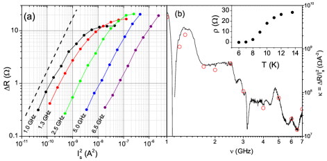
Fig.12(a) presents the dependence of the microwave induced change of the resistance on the square of the superconducting current at different frequencies as labeled. The response, which is similar to the one obtained on other samples, shows the strong decrease in the magnitude at high driving frequencies. Fig.12(b) presents the frequency dependence of the nonlinear coefficient =. The dependence is obtained in the regime of a small power at which the nonlinear response is proportional to the square of the superconducting current . The figure demonstrates again the strong reduction of the response to the applied microwave current at high driving frequencies.
At low frequency 1 GHz the obtained coefficient of nonlinearity is in accord with the one obtained in domain experiments in a similar sample (sample S2 in bo2013 ). The sample S2 has a slightly higher (1 K) transition temperature. In the experiments the nonlinear coefficient was obtained from the relation between the electric field and applied current density , where is the width of samples and is the nonlinear coefficient. The relation can be rewritten as yielding , where is the length of samples. At T=9K (corresponding to T=8K for Sample C) the nonlinear coefficient 5 (see Fig.3a in bo2013 ). It yields =1.5109 . This value is in a quantitative agreement with the one shown in Fig.12b at low frequencies. The correspondence between the nonlinear coefficients obtained by different experimental methods demonstrates that the reflection method provide a reasonable evaluation of the applied microwave current.
In conclusion, the presented reflection measurements indicate that the microwave radiation is quite uniformly coupled to the superconducting electrons at different frequencies. Analyzed in terms of the applied superconducting current the nonlinear response demonstrates significant reduction at high driving frequencies.
References
- (1) V. L. Berezinskii, Sov. Phys. - JETP 34, 610 (1972).
- (2) J. M. Kosterlitz and D. J. Thouless, J. Phys. C 6, 1181 (1973).
- (3) J. M. Kosterlitz and D. J. Thouless, J. M. Kosterlitz and D. J. Thouless, Progress in Low Temperature Physics (Elsevier, Amsterdam, 1978), vol. 7, Part 2, pp. 371-433.
- (4) J. V. Jose, ”40 years of Berezinskii-Kosterlitz- Thouless Theory”, (World Scientific, 2013).
- (5) B. I. Halperin and D. R. Nelson, J. Low Temp. Phys. 36, 599 (1979).
- (6) B. A. Huberman, R. J. Myerson and S. Doniach, Phys.Rev. Lett. 40, 780 (1978).
- (7) V. Ambegaokar, B. I. Halperin, D. R. Nelson and E. D. Siggia, Phys. Rev. B 21, 1806 (1980).
- (8) K. Epstein, A. M. Goldman and A. M. Kadin, Phys. Rev. Lett. 47, 534 (1981).
- (9) A. M. Kadin, K. Epstein, and A. M. Goldman, Phys. Rev. B 27, 6691 (1983).
- (10) A.T. Fiory, A. F. Hebard, and W. I. Glaberson, Phys. Rev B 28, 5075 (1983).
- (11) A. M. Goldman, ”40 years of Berezinskii-Kosterlitz-Thouless Theory: The Berezinskii-Kosterlitz-Thouless Transition in Superconductors,” J. V. Jose, (World Scientific, 2013), 135-160.
- (12) A. Gurevich and V. M. Vinokur, Phys. Rev. Lett. 100, 227007 (2008).
- (13) V. G. Kogan, Phys.Rev, B 75, 064514 (2007).
- (14) I. Hetel, T. R. Lemberger and M. Randeria, Nature Physics 3, 700 (2007).
- (15) B. Wen, R. Yakobov, S. A. Vitkalov and A. Sergeev, Appl. Phys. Lett. 103, 222601 (2013).
- (16) A. Gozar, G. Logvenov, L. Fitting Kourkoutis, A. T. Bollinger, L. A. Giannuzzi, D. A. Muller and I. Bozovic, Nature 455, 782 (2008).
- (17) G. Logvenov, A. Gozar, and I. Bozovic, Science 326, 699 (2009).
- (18) A. T. Bollinger, G. Dubuis, J. Yoon, D. Pavuna, J. Misewich and I. Božović, Nature 472, 458 (2011).
- (19) V. A. Gasparov and I. Bozovic, Phys. Rev B 86, 094523 (2012).
- (20) L. S. Bilbro, R. Valdes Aguilar, G. Logvenov, O. Pelleg, I. Bozovic, N. P. Armitage, Nature Physics 7, 298 (2011).
- (21) See Supplemental Material.
- (22) L. D. Landau and E. M. Lifshitz,”Course of Theoretical Physics: Mechanics” (Pergamon Press, 1976), 3rd Edition, Volume 1, 93.
- (23) M. J. Stephen and J. Bardeen, Phys. Rev. Lett. 14, 112 (1965).
- (24) G. E. Volovik, JETP Lett. 65, 217 (1997).
- (25) R. W. Crane, N. P. Armitage, A. Johansson, G. Sambandamurthy, D. Shahar, and G. Gruner, Phys. Rev. B 75, 094506 (2007).
- (26) Haruhisa Kitano, Takeyoshi Ohashi, and Atsutaka Maeda, Rev. Sci. Instrum. 79, 074701 (2008).