Coupling Tension and Shear for Highly Sensitive Graphene-Based Strain Sensors
Abstract
We report, based on its variation in electronic transport to coupled tension and shear deformation, a highly sensitive graphene-based strain sensor consisting of an armchair graphene nanoribbon (AGNR) between metallic contacts. As the nominal strain at any direction increases from 2.5 to 10%, the conductance decreases, particularly when the system changes from the electrically neutral region. At finite bias voltage, both the raw conductance and the relative proportion of the conductance depends smoothly on the gate voltage with negligible fluctuations, which is in contrast to that of pristine graphene. Specifically, when the nominal strain is 10% and the angle varies from to , the relative proportion of the conductance changes from 60 to 90%.
Graphene has been proposed for many applications due to its unique physical properties graphene1 ; graphene2 ; graphene3 ; gas-detector , in which the electronic transport through graphene nanoribbon would be affected by line defect R1 . Of specific interest to the present work, it has been proposed as a strain sensor due to change in the conductivity of graphene-based materials strain-e1 ; strain-e2 ; strain-e3 ; strain-e4 ; strain-e5 ; strain-simulation1 ; strain-simulation2 . The field of graphene-based strain sensing has rapidly developed since the experimental observation of the increase in resistance of CVD graphene samples when strain is applied in the direction of the electrical current strain-e1 . In order to accurately determine the direction and magnitude of strain, a triaxial graphene-based strain sensor composite was proposed; it was found that the resistance of graphene may be enhanced or reduced by the strain in certain directions strain-e2 . The sensitivity of graphene to strain originates from the deformation of carbon-carbon bonds, which alter the hopping integrals, and thus the electronic transport in graphene.
Though the effect of strain on the band structure of graphene and narrow graphene nanoribbons (GNRs) has been widely discussed strain-TB ; strain-band structure1 ; strain-band structure2 ; strain-band structure3 ; R2 , strain sensing based on electronic transport through graphene and GNRs has recently become of wide interest strain-transport1 ; strain-transport2 ; strain-transport3 ; strain-transport4 ; strain-transport-GNR1 ; strain-transport-GNR2 ; strain-transport5 . In the present work, motivated by recent experimental findings of the potential benefits of coupled tension/shear deformation to simulate the strain generated due to the movement of human fingers strain-e2 , we theoretically study coupled tension and shear deformation on the transport through armchair graphene nanoribbons between metallic contacts.


Most previous theoretical studies of graphene strain sensors have adopted homogeneous junctions. However, no lattice mismatch occurs at the interfaces for homogeneous junctions, whereas the conductance in unstrained GNRs is either zero or one at the Fermi energy conductance-GNRs . Unlike most experiments in which the gate voltage is only applied to graphene samples, the Fermi energy should vary to investigate electronic transport through GNRs. For heterogenous junctions of GNRs between quantum wire contacts, transport through GNRs is mediated by the gate voltage as in previous experimental measurement on electrical properties of graphene samples graphene1 ; graphene2 ; graphene3 . These heterogenous junctions are inspired by the fact that the contacts are metallic rather than carbon in experiments graphene1 ; graphene2 ; graphene3 and the conductance of quantum wire contacts is maximal at because all channels are available to electronic transport.
However, lattice mismatch may exist at the interfaces of heterogeneous junctions. Here we adopt heterojunctions of armchair-edged GNRs (AGNR) between quantum wire contacts as discussed in Ref. tm2 to minimize the effect of lattice mismatch at the interfaces and investigate the effect of uniaxial plus shear strain on electronic transport as illustrated in Fig. 1. The strain is only applied to the AGNR and impacts the hopping integrals in the AGNR. The hamiltonian of the AGNR and contacts is described by the tight binding approximation as
| (1) |
where a pair of integers indicates the lattice position , and () is the electron annihilation (creation) operator. The summation is over the nearest neighbors indicated by . is the hopping integral between nearest-neighboring sites indexed by and . is the effective gate voltage applied to graphene, which is zero in contacts. When slightly varies at the interfaces, the conductance does not change much around note1 .
The deformed configurations of the graphene nanoribbons were obtained by molecular mechanics simulations, where the strain was obtained via applied displacement loading strain-transport4 ; strain-Qi02 . The rectangular AGNR consisted of 2832 atoms with a length of nm and width nm. Displacements were applied in increments of 0.01Å followed by a subsequent energy minimization and relaxation until the change in system energy was less than compared with the previous step. The simulations were performed using the open source package LAMMPS lammps , and the AIREBO interatomic potential potential with a cutoff of nm. This potential has been shown to accurately describe carbon-carbon interactions resulting in accurate predictions of the mechanical properties of graphene MM-simulation . We note that because molecular mechanics simulations were performed, which are intrinsically at 0K, and because all applied displacements were in-plane, there was no out-of-plane buckling during the simulation.
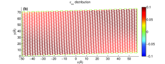
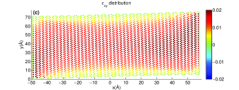
As shown in Fig. 1 (b,c), coupled tension and shear were applied onto AGNRs and the corresponding strains were calculated as discussed in previous works strain-transport4 . We also define the ‘nominal strain’ as the displacement applied (regardless of the direction) with reference to the original length. Once the carbon atomic positions are obtained at each value of strain, the hopping along each bond (with the length ) strain-TB ( eV and nm) is used as the basis for the electronic structure and quantum transport calculations. Due to the 2D nature of our analysis, bonds were not considered in our calculation.
Strain was applied with a tilted angle (Fig. 1) from to at five different angles, i.e. , , , and , where loading represents pure tension, represents pure shear and the other three couple tension and shear. To simplify the notation, we also introduce a ‘nominal strain’ , which is defined as the displacement applied over the original nanoribbon length regardless of the loading angle. All cases with different loading angles are deformed at three stages, namely , and we will refer exclusively to in the following. The tension () and shear () strain components at the three stages for different loading angles are corresponding as: and for ; and for ; and for ; and for ; and for . The deformed atomic configuration and the resulting components of the tensile and shear strain at when the nominal strain is is shown in Fig. 1(b) and (c) graphene-MM-BU . The left contact is fixed while the right one is shifted with strain similar to Ref. strain-e4 when the shear strain is present, and the hopping integral in contacts and interfaces are not affected by the shear/tension.

At a finite bias voltage , the current transfer from the left contact to the right one is expressed as Landauer , where refers to the strain and stands for no deformation in the GNR, e is the electron charge and is Planck’s constant. is the transmission at the strain , the energy and the gate voltage . Since the effect of the gate voltage on the strain sensor has been explored in a dual-gate setup strain-e4 , we include to estimate the stability and applicability of the graphene-based strain sensor. Based on the tight binding hamiltonian in Eq.(1) and the transfer matrix method, the transmission is obtained through the scattering matrix by solving the Schrdinger equations, which is described in detail in Refs. tm3 ; tm4 .
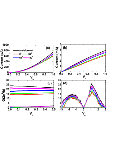
at at first increases slowly and then sharply with as shown in Fig. 2 (a), since the transmission increases as the GNR deviates from being electrically neutral, which has the lowest density of states strain-transport5 . at at first increases linearly and then sub-linearly with as shown in Fig. 2 (b), since the transmission decreases as GNR deviates from the highest density of states strain-transport5 . The conductance is defined as , and is directly related to the transmission at Fermi energy at the limit of Landauer . The conductance slightly increases and decreases at and respectively when increases, as shown in Fig. 2(c). When changes, a large oscillation of the conductance at is induced by quantum interference when electrons are reflected at the GNR-contact interfaces strain-transport5 ; tm2 ; tm1 ; tm3 ; tm4 , and electron-hole asymmetry in conductance is originated by odd-numbered rings at the interfaces as shown in Fig. 1 tm2 . The curve of the conductance versus the gate voltage at overlaps the one at and the fluctuation becomes invisible, as shown in Fig. 2(d), due to the summation of the transmission among the energy range .
In strained AGNRs, the transport depends on both the direction and magnitude of the strain . When the nominal strength of the strain is , the current at both zero and finite is lower than in undeformed AGNR, and gradually increases with the change in angle of the applied strain, when the strain varies from to combined with shear, as shown in Fig. 2(a,b). Under pure tension at , the change in the current completely reproduces the observation strain-e1 . The slope of the - curve (i.e., the conductance) for nearly electrical neutral graphene samples, which corresponds to our result at and which is dependent on the specific experimental setup, is strain-e1 and strain-e2 . Our results show that the ballistic conductance of the 7.018 nm wide AGNR is around and at and respectively. The conductance dependence on the strain shown in Fig. 2(c) is the same as the current dependence on the strain.
We compare the conductance dependence on pure tension and pure shear at to estimate the effect of tension and shear on transport through AGNR. On one hand, in contrast to the fact that the conductance at under pure tension at is higher than undeformed AGNRs as a result of an increase in the hopping integrals along the horizontal direction strain-transport5 , the conductance under pure shear at is always lower than that in undeformed AGNRs as except for some fluctuations as shown in Fig. 2. Our calculation is consistent with the observation of the conductance dependence on the shear strain strain-e4 . On the other hand, the conductance around the neutral point (i.e., at small ) increases with the angle of tension/shear as shown in Fig. 2(c), compared with that under pure tension at . The maximal conductance of undeformed AGNR being () occurs at and between graphite contacts and at and between quantum wire contacts. The maximal conductance of strained AGNR around decreases as a result of deformation in AGNR when tension and/or shear is applied to AGNR. The data indicates that electronic transport through AGNR can be easily mediated by the strain when the system deviates from the electrically neutral region.

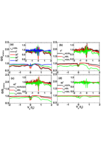
In most experiments of graphene-based strain sensors strain-e1 ; strain-e2 , no gate voltage is applied and graphene may not be electrically neutral due to the doping from metallic contacts strain-e4 ; dop-contact . Recently the effect of the gate voltage has been explored strain-e4 , and thus we set the gate voltage as a variable parameter to provide information such as the stability of the strain sensor under different gate voltages. The change of current is usually measured under strain and the percentage of the resistance is used to estimate the effect of the strain on transport through graphene samples strain-e1 ; strain-e2 . Therefore, we use the ratio of the conductance compared with that in undeformed AGNR, , to measure the sensitivity of the graphene-based strain sensor as shown in Fig. 3.
Due to large oscillations in the conductance at , a large oscillation is also seen in the ratio as shown in the insets of Fig. 3. However, the trends of are still clear. The conductance ratio at shown in the main panels of Fig. 3 is relatively smooth at negative gate voltage, shows a large dip or peak around zero gate voltage and slightly decreases as the gate voltage becomes more positive. When the nominal strain is 10% in Fig. 3(a), the conductance slightly increases but is smaller than in the undeformed case, as the angle varies from 0∘ to 90∘. As is varied from 0∘, 45∘ and 90∘ in Figs. 3(b-d), the conductance decreases as the nominal strain increases from 2.5% to 10%. It is found that the conductance shows little change under pure shear at 90∘ as shown in Fig. 3(d). We demonstrate that this kind of strain sensor is robust since the relative proportion of the conductance is smooth within a wide gate voltage range graphene1 ; graphene2 .
In summary, we have studied a graphene-based strain sensor consisting of armchair graphene nanoribbon (AGNR) between metallic contacts in response to combined tension/shear. The conductance and the relative proportion of the conductance decreases as the strain increases. This kind of strain sensor has relatively higher sensitivity to the strength of the strain at finite bias voltage and a wide range of the gate voltage when the strain is parallel to the armchair edge.
Finally we comment on the performance of a strain sensor made from a zigzag graphene nanoribbon (ZGNR) between quantum wire contacts with a possible lattice mismatch at the interfaces. Compared with the case of AGNR, the fluctuation of the conductance of ZGNR is larger, when the gate voltage changes. The ratio of the conductance, , ranges between 0.8 and 1.4 as , and the dependence of the conductance ratio on the strain are different from that seen in Fig. 3 when .
Acknowledgements HSP and ZQ acknowledge support from the Mechanical Engineering and Physics Departments at Boston University. G. P. Zhang thanks support by NSF of China (Grant No. 11204372).
References
- (1) Novoselov K S, Geim A K, Morozov S V, Jiang D, Zhang Y, Dubonos S V, Grigorieva I V and Firsov A A 2004 Science 306, 666
- (2) Novoselov K S, Geim A K, Morozov S V, Jiang D, Katsnelson M I, Grigorieva I V, Dubonos S V and Firsov A A 2005 Nature (London) 438, 197
- (3) Miao F, Wijeratne S, Zhang Y, Coskun U C, Bao W and Lau C N, 2007 Science 317 1530
- (4) Schedin F, Geim A K, Novoselov K S et al 2007 Nature Materials 6, 652-655
- (5) Dutta P, Maiti S K and Karmakar S N 2013 J. Appl. Phys. 114(3), 034306.
- (6) Fu X W, Liao Z M, Zhou J X, Zhou Y B, Wu H C, Zhang R, Jing G Y, Xu J, Wu X S, Guo W L and Yu D P 2011 Appl. Phys. Lett. 99, 213107
- (7) Bae S H, Lee Y, Sharma B K, Lee H J, Kim J H and Ahn J H 2013 Carbon 51, 236
- (8) Chun S, Kim Y, Jin H, Choi E, Lee S B and Park W 2014 Carbon 78, 601-608
- (9) He X, Gao L, Tang N et al 2014 Appl. Phys. Lett. 105, 083108
- (10) Wang Y, Wang L, Yang T T et al 2014 Adv. Funct. Mat. 24, 4666-4670
- (11) Souma S, Ohmi Y, Ogawa M 2013 J. Comput. Electr. 12, 170-174
- (12) Mohammad Reza Moslemi, Mohammad Hossein Sheikhi, Kamyar Saghafi, Mohammad Kazem Moravvej-Farshi 2012 Microelectronics Reliability 52, 2579-2584
- (13) Pereira V M, Neto A H Castro and Peres N M R 2009 Phys. Rev. B 80, 045401
- (14) Li Y, Jiang X W, Liu Z F and Liu Z R 2010 Nano Res. 3, 545
- (15) Peng X, Tang F and Copple A 2012 J. Phys.: Condens. Matter 24, 075501
- (16) Lu Y and Guo J 2010 Nano Res. 3, 189
- (17) Sena S H R, Pereira Jr J M, Farias G A, Peeters F M and Costa Filho R N 2012 J. Phys. Condens. Matter, 24(37), 375301
- (18) Poetschke M, Rocha C G, Torres L E F Foa, Roche S and G. Cuniberti 2010 Phys Rev B 81, 193404
- (19) Wang J Y, Liu Z F and Liu Z R 2012 AIP Advances 2, 012103
- (20) Rasuli R, Rafii-Tabar H and Zad A I 2010 Phys Rev B 81, 125409
- (21) Qi Zenan, Bahamon D A, Perira Vitor M, Park Harold S and Campbell D K 2013 Nano Lett. 13, 2692-2697
- (22) Bahamon D A and Pereira V M 2013 Phys. Phys. Rev. B 88, 195416
- (23) Cosma Diana A, Mucha-Kruczy ski Marcin, Schomerus Henning and Vladimir I. Fal’ko 2014 Phys. Rev. B 90, 245409
- (24) Wang J, Zhang G P, Ye F and Wang X Q arXiv:1411.1529
- (25) Peres N M R, Castro Neto A H and Guinea F 2006 Phys Rev B 73, 195411
- (26) Zhang G P and Qin Z J 2011 Chem. Phys. Lett. 516, 225
- (27) Wang J, Zhang G P, Ye F and Wang X Q unpublished.
- (28) Qi Z, Campbell D K and Park Harold S 2014 Phys. Rev. B 90, 245437
- (29) http://lammps.sandia.gov (2012); Plimpton S 1995 J. Comput. Phys. 117, 1
- (30) Stuart S J, Tutein A B and Harrison J A 2000 J. Chem. Phys. 112, 6472
- (31) Zhao H, Min K, Aluru N R 2009 Nano Lett. 9, 3012-3015; Wang M et al 2012 Comput. Mater. Sci 54, 236-239
- (32) Qi Z, Kitt Alexander L, Park Harold S, Pereira Vitor M, Campbell David K and Neto A H Castro 2014 Phys. Rev. B 90, 125419
- (33) Los J H, Katsnelson M I, Yazyev O V, Zakharchenko K V and Fasolino A 2009 Phys. Rev. B 80, 121405
- (34) Bttiker M, Imry Y, Landauer R and Pinhas S 1985 Phys. Rev. B 31, 6207
- (35) Yin Y and Xiong S J 2003 Phys. Lett. A 317, 507
- (36) Hu S J, Du W, Zhang G P, Gao M, Lu Z Y and Wang X Q 2012 Chin. Phys. Lett. 29, 057201
- (37) Gao M, Zhang G P and Lu Z Y 2014 Comput. Phys. Commun. 185, 856
- (38) Giovannetti G, Khomyakov P A, Brocks G, Karpan V M, Brink J van den and Kelly P J 2008 Phys. Rev. Lett. 101, 026803