Hexagonal AlN: Dimensional-Crossover-Driven Bandgap Transition
Abstract
Motivated by a recent experiment that reported the successful synthesis of hexagonal (h) AlN [Tsipas et al. Appl. Phys. Lett. 103, 251605 (2013)] we investigate structural, electronic and vibrational properties of bulk, bilayer and monolayer structures of h-AlN by using first-principles calculations. We show that the hexagonal phase of the bulk -AlN is a stable direct-bandgap semiconductor. Calculated phonon spectrum displays a rigid-layer shear mode at 274 cm-1 and an Eg mode at 703 cm-1 which are observable by Raman measurements. In addition, single layer -AlN is an indirect-bandgap semiconductor with a nonmagnetic ground state. For the bilayer structure, AA′ type stacking is found to be the most favorable one and interlayer interaction is strong. While N-layered -AlN is an indirect bandgap semiconductor for N=1-10, we predict that thicker structures (N10) have a direct-bandgap at the -point. The number-of-layer-dependent bandgap transitions in -AlN is interesting in that it is significantly different from the indirect-to-direct crossover obtained in the transition metal dichalcogenides.
pacs:
81.05.ue, 85.12.de, 68.47.Fg, 68.43.Bc, 68.43.FgI Introduction
Bulk structures of III-V semiconductors have been widely studied due to their importance for technological applications such as blue light-emitting diodes, lasers operating in the blue and the ultraviolet regime, high temperature diodes and transistorsyeh1 ; yeh2 ; morkoc ; vurgaftman ; fukumoto ; christensen . In addition, technological advances lead to the emergence of novel low-dimensional forms of III-V binary compounds. Experimental fabrication of AlN nanowireswu1 ; duan ; zhao ; li , nanobeltswu2 ; tang ; yu and nanodotsgoh ; bouch have already been reported. In recent years, theoretical and experimental studies of graphenenovo1 provided a wide range of knowledge for a new class of materials and have opened up possibilities for the synthesis of many similar structures such as; silicene kara ; liu ; cahangirov ; sw , germanene cahangirov ; ni ; dav ; yang , transition metal dichalcogenides (TMDs) mx2-0 ; mx2-1 ; mx2-2 ; mx2-3 ; exp-ws ; st-mose ; hs-wse ; hs-res and hexagonal structures of III-V binary compounds (e.g. -BN, -AlN) hasan1 ; zhuang-hennig ; wang ; kim ; farahani . Among the binary compounds, after single layer BN, AlN is currently a material of much interest due to its semiconducting nature and its large bandgap which is suitable for device applications.
Following the first theoretical study on the stability of hexagonal AlN reported by Sahin et al.hasan1 , successful experimental realization of hexagonal AlN phase was achieved very recently by Tsipas et al.tsipas In the early study of Du et al., energetic and electronic properties of one-dimensional AlN nanostructures such as nanowires with hexagonal cross sections, double-and triple-walled faceted nanotubes and single-walled faceted AlN nanotubes were investigated.du Between the first theoretical prediction and the experimental realization of -AlN, other groups have also focused on this material. Zheng et al.zheng predicted that zigzag AlN nanoribbons have an indirect bandgap whereas armchair AlN nanoribbons have a direct bandgap, and these bandgaps monotonically decrease with increasing ribbon width. Almeida et al.almeida studied the energetics and electronic properties of typical defects in a -AlN network such as vacancies, anti-sites and impurities. It was shown that defects such as N vacancies and Si impurities lead to the breaking of the planar symmetry of the -AlN sheet and significant changes in the band structure in the vicinity of the Fermi level. In addition, Chen et al. systematically investigated the electronic structure of armchair and zigzag AlN, GaN nanoribbons and investigated also the electronic properties of AlN/GaN nanoribbon heterojunctions. They found that the bandgap of both nanoribbons decrease monotonically as the ribbon widths increase and that the bandgap of the nanoribbon heterojunctions are closely related to the AlN/GaN ratiochen . Shi et al. calculated the magnetic properties of undoped and transition metal (TM) doped AlN nanosheets by using first-principles calculations. They reported that AlN nanosheet is nonmagnetic, whereas a single TM atom can bring about large local magnetic moments in TM-doped AlN nanosheetsshi .
Motivated by the recent study of Tsipas et al.tsipas reporting the formation of stable h-AlN phases at the early stages of AlN growth, we aim to address the following experimental observations: (i) modification in electronic valence band structure, (ii) relatively large lattice parameter that was reported as an indication of h phase, (iii) reduction in band gap in comparison with bulk wurtzite, and (iv) dynamical stability of h-AlN.
Our study reveal that the synthesized -AlN, although it has structural similarities, electronically displays different characteristics from -BN and TMDs. As well as weak van der Waals (vdW) interactions, ionic character of the interlayer interactions plays an important role in the electronic properties of mutilayered -AlN. Therefore, while monolayers of -BN and TMDs are direct band gap semiconductors, -AlN has an indirect band gap. In addition, upon dimensional reduction from bulk to bilayer energy the band gap decreases like as was found for -BN and TMDs.
The paper is organized as follows: in Sec. II we give details of our computational methodology. In Sec. III we briefly overview the structural and electronic properties of hexagonal AlN (h-AlN) structure together with wurtzite structure. In Sec. IV stability of few layer structures and their electronic properties are investigated in details. Our findings are discussed in Sec. V
II Computational Methodology
Our investigations of the minimum energy configurations of different AlN structures and their electronic properties, were carried out using the Vienna ab-initio simulation package VASP.vasp1 ; vasp2 ; vasp3 ; vasp4 which is based on density functional theory (DFT). The VASP code solves the Kohn-Sham equationsKohn-Sham for a system with periodic boundary conditions using plane-wave basis set iteratively. The Perdew-Burke-Ernzerhof (PBE) form of the Generalized Gradient Approximation (GGA)GGA-PBE1 ; GGA-PBE2 was adopted to describe electron exchange and correlation. The band gap underestimation in bare GGA calculations are also examined by using the hybrid DFT-HSE06 functional.HSE06 The vdW interaction that is significant for layered -AlN material was taken into account for all multilayer structuresvdW1 ; vdW2 . For the charge transfer analysis the Bader technique was usedHenkelman .
The kinetic energy cut-off of the plane-wave basis set was eV in all calculations. The optimization of atomic positions was performed by minimizing the total energy and the forces on the atoms hence the energy difference between sequential steps was taken eV as a convergence criterion in the structural relaxation, and the convergence for the Hellmann-Feynman forces on each atom was taken to be eV/Å. In addition, Gaussian smearing factor of eV was used for non-self-consistent calculations and the pressures on the unit cell were decreased to a value less then 1.0 kB in all three directions. For the determination of accurate charge densities, Brillouin zone integration was performed using a Monkhorst-Pack mesh for the primitive unit cellMonkhorst . To avoid interaction between adjacent AlN monolayers and few layer systems, our calculations were performed with a large unit cell including Å vacuum space. We also calculated the cohesive energy (Ecoh) which was formulated as , where , , , , and are the total energy per unitcell, the energy of free Al atom, the energy of free N atom, number of Al and N atoms in unitcell, respectively.
III Structures of Bulk AlN
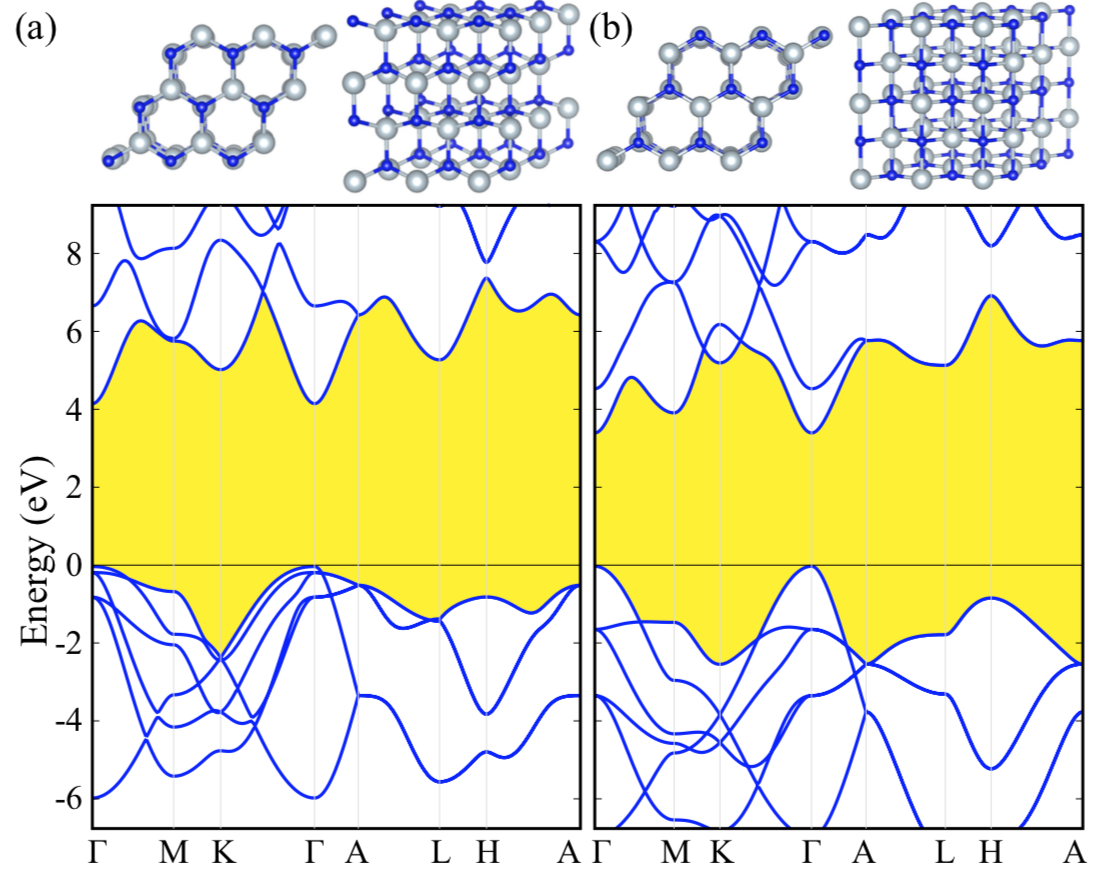
First we briefly overview the characteristics of wurtzite and recently synthesized -AlN before the extensive investigation of the number of layer dependent properties of -AlN are undertaken. At ambient conditions, AlN crystallizes in a wurtzite () structure that belongs to the space group. As shown in Table 1, PBE approximation gives the following structural parameters Å and . In the structure of AlN each Al-N bond is formed by 2.35 charge donation from Al to N atom and therefore it has a highly ionic character. In parallel with the abundance of the form of AlN in nature, among the possible bulk structures is the energetically most favorable one. The electronic dispersion shown in Fig. 1 indicates that -AlN is a semiconductor with a eV direct bandgap at the point.
| a | c | dLL | dAl-N | Ecoh | Egap | ||
|---|---|---|---|---|---|---|---|
| (Å) | (Å) | (Å) | (Å) | () | (eV) | (eV) | |
| Bulk -AlN | 3.11 | 5.01 | - | 1.90 | 2.35 | 6.14 | 4.2 (d) |
| Bulk -AlN | 3.30 | 4.15 | 2.08 | 1.90 | 2.37 | 6.02 | 3.4 (d) |
| 2L -AlN | 3.20 | - | 2.13 | 1.85 | 2.32 | 5.73 | 3.5 (i) |
| 1L -AlN | 3.13 | - | - | 1.81 | 2.28 | 5.36 | 2.9 (i) |
In addition to some early theoretical predictionshasan1 the stability of the hexagonal phase of AlN (-AlN) was proven by a very recent experimental study.tsipas Regarding the less layered structures or surfaces of wurtzite materials, transformation from wurtzite to a graphite-like structure that allows the removal of destabilizing dipoles is energetically more favorable.freeman This graphite-like hexagonal structure of AlN belongs to the space group. The layered planar structure has two atoms in the unitcell which has lattice vectors , and where . Atomic coordinates are and , for first and second type of atoms respectively. We considered that the layers are AA′ stacking (deciding the stacking of layers is explained in Section IV-B) which is shown in Fig.1(b). And we found that the lattice constant is Å and the distance between layers is Å which is smaller when compared to graphite and -BN ( Å and Å for graphiteBaskin ; Chung and -BNPaszkowicz ; Marini ; Shi , respectively). Intraleyer atomic distance between Al and N atoms is Å. This is the same as for -AlN. The cohesive energies are given in Table 1.
As shown in Fig. 1(d), layered -AlN is a direct bandgap semiconductor which has eV bandgap with band edges located at the point. Therefore, our results confirm the experimentally reported bandgap reductiontsipas in -AlN compared to bulk -AlN. At the top of the VB, there is a single parabolic band for holes and the main contributions are from the orbital of N atoms. The bottom of the CB, there is a single parabolic band and most of the states come from orbital of N atoms. Final charges of Al and N atoms are 0.63 and 7.37 , respectively. Therefore, 2.37 charges are transferred from Al to N atom. Following section is devoted to the understanding of the characteristics of monolayer -AlN and the nature of the inter-layer interactions.
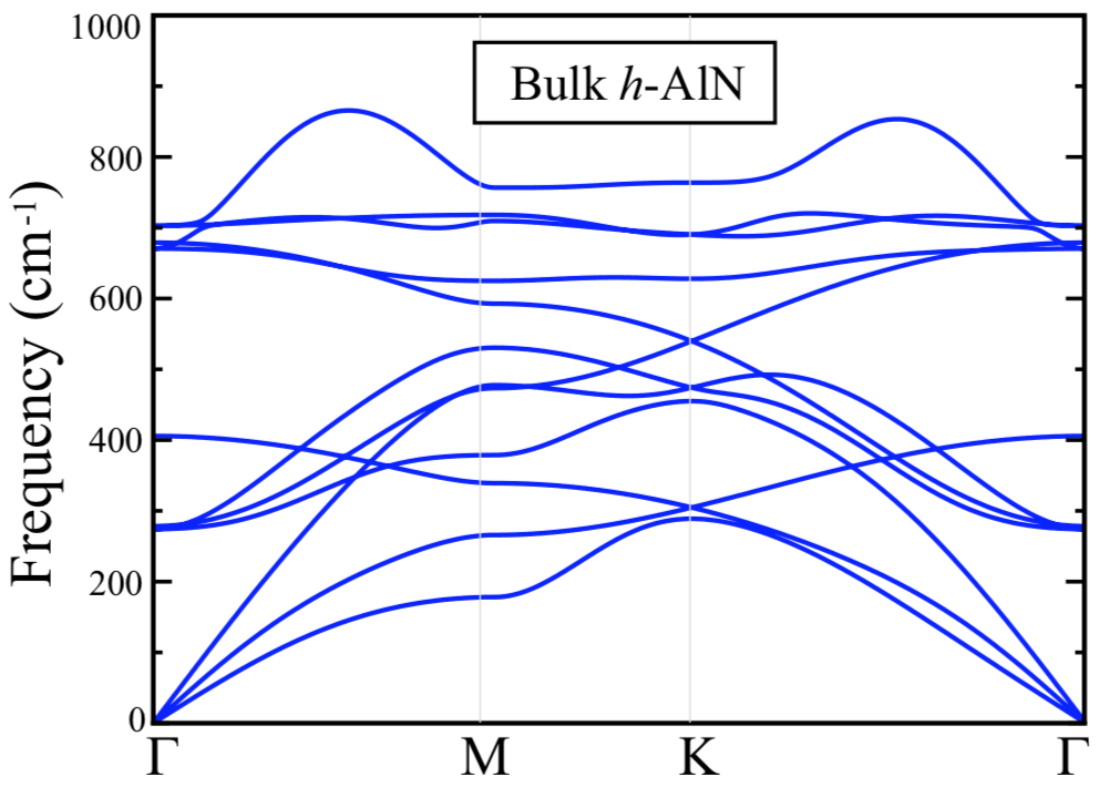
Lastly, we analyze vibrational properties of the -AlN phase by calculating the phonon spectrum in whole Brillouin Zone (BZ) using the small displacement methodologyalfe for 32-atomic supercell. As shown in Fig. 2 phonon spectrum of -AlN displays real eigenfrequencies in the whole BZ. Therefore, there is no doubt on the dynamical stability of the -AlN structure. Here we also see that differing from its -BN counterpart the optical and acoustical modes couple with each other at certain points in the BZ. In the case of -AlN, there are 4 atoms per primitive unit-cell and 12 phonon branches. The first three are acoustical phonon modes, the phonon branch at 274 cm-1 is a doubly degenerate rigid layer shear mode, known as low-energy Eg mode, involving the out-of-phase motion of atoms in adjacent planes. In addition, the highly dispersive phonon modes with eigenvalues 406 and 679 cm-1 at the zone center correspond to out-of-phase motion of Al and N atoms in adjacent layers. Interestingly, the contribution of the second atom type in these modes are negligibly small. The highest optical mode, doubly degenerate at the point, have the Eg symmetry and therefore it is expected to be measured in Raman experiments.
IV Monolayer, Bilayer and Few Layer -AlN
IV.1 Monolayer -AlN
The first prediction of the dynamical stability and electronic properties of single layers of -AlN and similar III-V compounds were first reported by Sahin et al.hasan1 Monolayer hexagonal structure belongs to the space group with unit vectors , where . In this configuration the atomic coordinates are given as and for first and second type of atoms, respectively. We calculated that the lattice constant of monolayer -AlN is Å and the distance between Al and N atoms is Å which is the lowest value when compared with bulk forms and bilayer structure as seen from Table 1. These results are in good agreement with the measured lattice parameters (3.13 Å) of epitaxially grown of -AlN, at early stages, by Tsipas et al.tsipas . The cohesive energy of monolayer -AlN is the lowest among the possible phases. It is also seen that the amount of charge transfer from Al to N slightly decreases from bulk to monolayer -AlN.
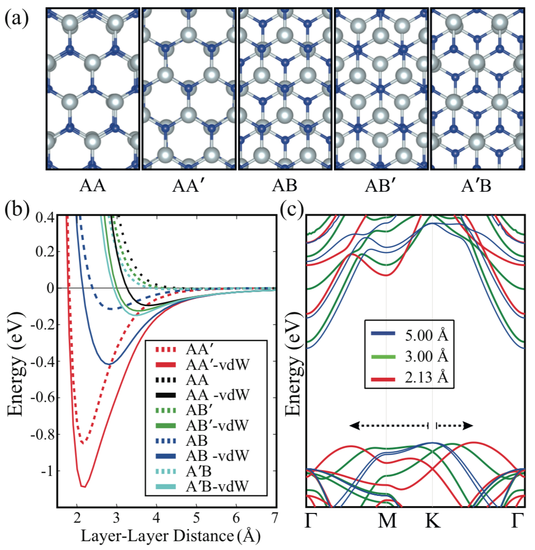
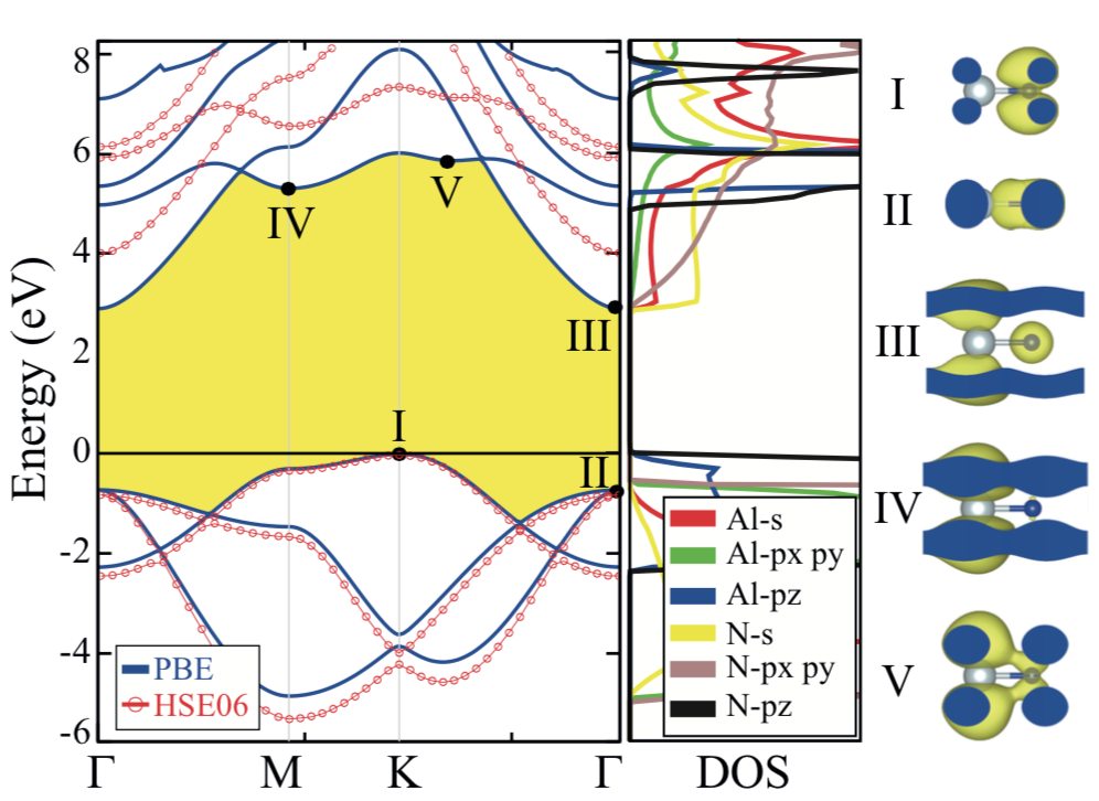
Fig. 3 illustrates the band diagrams, density of states and also the 3D charge densities of states at the band edges for monolayer -AlN. Differing from bulk -AlN which has a direct bandgap at the , the VBM of the monolayer is at the K point and the CBM is at the point, therefore monolayer -AlN is an indirect bandgap insulator with eV bandgap. It is also seen that bare-GGA and DFT-HSE06 approximated electronic band dispersions shown in Fig. 3 are almost the same. With DFT-HSE06 hybrid functional, -AlN is an indirect bandgap material with a bandgap of eV. It is also noteworthy to mention that -BN is the counterpart of AlN with a direct bandgap at the K point.
Right panel of Fig.3 shows that the bonding states at VBM (label I) are mainly composed of N- orbitals and the degenerate state, with lower energy, at the point (label II) stems from hybridized and orbitals. In addition, the CBM located at the point has a quadratic-like dispersion (label III) and the relevant charge density is in the form of surface state. Therefore, the conduction electrons in single layer -AlN display free-electron-like behavior. Moreover the anti-bonding states with higher energy at the M and the K points are composed by mainly Al and slightly N states together.
IV.2 Bilayer -AlN and Layer-layer Interaction
During the growth of lamellar materials prediction of the most preferable stacking sequence is of importance. To determine the stacking order of bilayer AlN, we examined five possible (see Fig. 4(a)) stacking types: AA (Al over Al and N over N), AA′ (Al over N and N over Al), AB (Al over N and N over center of hexagon), A′B (Al over Al and N over center of hexagon), AB′ (N over N and Al over center of hexagon).
To determine the interaction strength and interlayer interaction profile of above-mentioned stacking orders of bilayer -AlN, total energies were calculated as a function of layer-layer distance. As seen from Fig. 4(b), the largest interlayer coupling energy and shortest interlayer distance is obtained for AA′ type stacking. Therefore AA′ stacking corresponds to the ground state stacking order. It is also seen that the vdW correction to the interaction energy is 250 meV per unitcell. In addition, for AA′ stacking, layer-layer distance is Å which is the minimum value among all stacking combinations. Here it appears that due to the presence of surface states interlayer distance in bilayer -AlN is slightly larger than that of bulk -AlN. However, compared to graphiteBaskin ; Chung and -BNPaszkowicz ; Marini ; Shi , and their bilayer forms, -AlN has a smaller interlayer distance. The lattice parameter, Å, which is the maximum value of all stacking combinations that slightly differs from the value obtained by self-correlation analysis of the experimental data (3.140.06) for few layers. This slight disagreement can be understood from the effect of the Ag(111) substrate.
| K | M | K | Ecoh | |||||
|---|---|---|---|---|---|---|---|---|
| 1L AlN | 3.62 | 2.92 | - | - | 5.36 | |||
| 2L AlN | 4.29 | - | 3.61 | 3.53 | 5.73 | |||
| 3L AlN | 4.05 | 3.58 | 3.57 | 3.53 | 5.82 | |||
| 4L AlN | 3.79 | - | 3.51 | 3.50 | 5.86 | |||
| 5L AlN | 3.61 | 3.73 | 3.46 | 3.46 | 5.89 | |||
| 6L AlN | 3.48 | - | 3.41 | 3.41 | 5.92 | |||
| 7L AlN | 3.38 | 3.77 | 3.35 | 3.35 | 5.93 | |||
| 8L AlN | 3.33 | - | 3.30 | 3.30 | 5.94 | |||
| 9L AlN | 3.27 | 3.81 | 3.26 | 3.26 | 5.95 | |||
| 10L AlN | 3.22 | - | - | - | 5.96 |
Moreover, in Fig. 4(c), we analyze how the electronic band dispersion of AA′-stacked bilayer is modified with varying interlayer distance. Negligibly interacting, weakly interacting and highest interaction (ground state) cases are illustrated using layer-layer distances of 5.00, 3.00 and 2.13 Å, respectively. The band diagram of negligibly interacting case resembles the electronic structure of monolayer -AlN. However, when the layers start to interact, for instance in the weakly interacting case (delineated by green lines in Fig. 4(c)), the top of the VBM are shifted towards the zone center. When the interlayer distance reaches its optimum position, one of the VBM appears at K- while the other one is located at M-. Interestingly, the location of CBM in BZ is independent from the interlayer distance. Hence from monolayer to bilayer, the indirect character is conserved and the bandgap is changed from 2.9 to eV.
IV.3 Few Layer -AlN
Synthesis of stable ultra-thin -AlN structures, sub-monolayer to 12 layers, was demonstrated by Tsipas et al.tsipas , recently. Our first-principles total energy optimization calculations revealed that lamellar hexagonal structure of N-layered (N=1,2,…) AlN is a stable phase. As shown in Figs. 5 and 6, planarity of the few-layered structures is preserved, except the negligible buckling at the surface layers, while electronically few layer -AlN is significantly different from monolayer one.
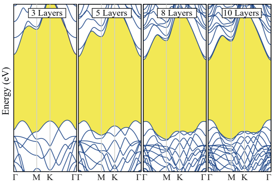
In order to illustrate how the electronic structure evolves with increasing number of layers we present the band dispersion of 3, 5, 8 and 10-layered -AlN in Fig. 5. Here there are several interesting trends that is worth to note: (i) the energy of the conduction band edge at the point decreases with increasing number of layers, (ii) states at conduction band edge which have surface state character remain unchanged. The energy difference between the band edges VBM() and CBM() increases from 2.92 eV for monolayer to 3.81 eV for 10-layer -AlN, and (iii) the most significant influence of additional number of layers is on the bonding states forming the valence band maximum at the M and the K points. It appears that due to the strong interlayer interaction each additional layer shifts these band edges towards the zone center. This gradual shift of VB edges continues up to 10 layers. Upon the formation of the 10th layer -AlN structure reaches the bulk limit and it becomes a direct band gap semiconductor. Increasing the thickness furthermore has no influence on the electronic properties of N-layered -AlN and they are direct bandgap ( eV for ten layered) materials like bulk -AlN. As given in detail in Table 2, transition energies between the points converge asymptotically to values of bulk -AlN. Increasing the number of layers, cohesive energies converge to that of bulk -AlN. It appears that only few layer -AlN structures with thickness N11 are suitable for lasing device applications. Here calculated modifications in electronic structure explains and supports the experimental findings of Tsipas et al.tsipas .
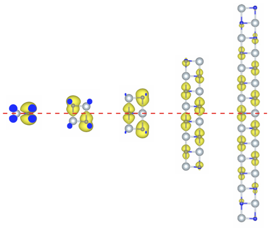
However, the evolution of the VBM with changing number of layers requires further attention. In Fig. 6 we present the 3D charge density of the electronic states located at the VBM. It is clearly seen that the character of the bonding state (VBM) is modified monotonically with increasing number of layers. With increasing number of layers the hybridization between N- states is weakened. In addition, due to the mild buckling the interaction of the surface states which have -like character and N- states vanishes at the vicinity of the upper- and the lower-most layers. Therefore for enough thick -AlN materials, which is found to be larger than 10-layers, the electronic structure is mainly determined by uniformly distributed N- states and hence the structure behaves like a bulk material having a direct bandgap at the symmetry point.
V Conclusions
Using first principles methodology, we investigated the thickness dependent electronic properties of layered hexagonal AlN. First, we showed that the bulk structure of hexagonal AlN is a semiconductor with a direct bandgap at the point. Phonon spectrum analysis of this structure reveals two Raman-active modes at 274 and 703 cm-1. Here, the lattice parameter of -AlN, which is larger than the wurtzite phase, agrees with the experiment of Tsipas et al.tsipas that reports the formation of hexagonal regions at the early stages of the growth process. Next, the formation of multilayer structures and most favorable stacking order were investigated via total energy calculations. It is seen that, similar to the hexagonal BN counterpart, among the possible stackings AA′ type stacking is the most favorable. It is worthwhile to note that the interlayer interaction is larger compared to similar layered materials with hexagonal lattice symmetry. Differing from some other two-dimensional crystal structures such as graphite, -BN and TMDs, here the ionic interlayer interaction is dominant between the -AlN layers. Therefore, for the synthesis of -AlN the epitaxial growth technique performed by Tsipas et al.tsipas appears more suitable than mechanical exfoliation.
Subsequently, the evolution of the electronic structure of N-layered -AlN was investigated for structures with 1-15 layers. It is seen that unlike bulk -AlN, monolayer -AlN has an indirect bandgap where VBM and CBM are at the K and the points, respectively. Moreover, it is seen that upon the formation of additional layers valence band edges gradually shift towards the Brillouin Zone center. Such a modification of the valence band states is in good agreement with the experiment of Tsipas et al.tsipas It was also calculated that the few layered structures reach the bulk limit and their electronic properties remains almost unchanged after the formation of 10 layers. Therefore, structures thicker than 10 layers, exhibits a direct band gap of 3.22 eV at the point. We believe that easy synthesis and the presence of a thickness-dependent bandgap crossover in few-layered hexagonal AlN structures are very important for novel device applications.
Acknowledgements.
This work was supported by the Flemish Science Foundation (FWO-Vl) and the Methusalem foundation of the Flemish government. Computational resources were provided by TUBITAK ULAKBIM, High Performance and Grid Computing Center (TR-Grid e-Infrastructure). C.B. and R.T.S. acknowledge the support from TUBITAK Project No 114F397. H.S. is supported by a FWO Pegasus Long Marie Curie Fellowship.References
- (1) —————————————–
- (2) C. Y. Yeh, Z. W. Lu, S. Froyen, and A. Zunger, Phys. Rev. B 45, 12130 (1992).
- (3) C. Y. Yeh, Z. W. Lu, S. Froyen, and A. Zunger, Phys. Rev. B 46, 10086 (1992).
- (4) H. Morkoc, S. Strite, G. B. Gao, M. E. Lim, B. Sverdlov, and M. Burns, J. Appl. Phys. 76, 1363 (1994).
- (5) I. Vurgaftman, J. R. Meyer, and L. R. Ram-Mohan, J. Appl. Phys. 89, 5815 (2001).
- (6) K. Miwa and A. Fukumoto, Phys. Rev. B 48, 7897 (1993).
- (7) N. E. Christensen and I. Gorczyca, Phys. Rev. B 50, 4397 (1994).
- (8) Q. Wu, Z. Hu, X. Z. Wang, Y. M. Hu, Y. J. Tian, and Y. Chen, Diamond Relat. Mater 13, 38 (2004).
- (9) J. H. Duan, S. G. Yang, H. W. Liu, J. F. Gong, H. B. Guang, X. N. Zhao, R. Zhang, and Y. W. Du, J. Phys. Chem. B 109, 3701 (2005).
- (10) Q Zhao, H. Z. Zhang, X. Y. Xu, Z. Wang, J. Xu, D. P. Yu, G. H. Li, and F. H. Su, Appl. Phys. Lett. 86, 193101 (2005).
- (11) Y. Li, J. Xiang, F. Qian, S. Gradecak, Y. Wu, H. Yan, H. Yan, D. A. Blom, and C. M. Lieber, Nano Lett. 6, 1468 (2006).
- (12) Q. Wu, Z. Hu, X. Z. Wang, and Y. Chen, J. Phys. Chem. B 107, 9276 (2003).
- (13) Y. B. Tang, H. T. Cong, F. Li, and H. M. Cheng, Diamond Relat. Mater 16, 537 (2007).
- (14) L. S. Yu, Y. Y. Lv, X. L. Zhang, Y. Y. Zhang, R. Y. Zou, and F. Zhang, J. Cryst. Growth 334, 57 (2011).
- (15) W. H. Goh, G. Patriarche, P. L. Bonanno, S. Gautier, T. Moudakir, M. Abid, G. Orsal, A. A. Sirenko, Z. H. Cai, A. Martinez, A. Ramdane, L. Le Gratiet, D. Troadec, A. Soltani, and A. Ougazzaden, J. Cryst. Growth 315, 160 (2011).
- (16) Z. Bouchkour, P. Tristant, E. Thune, C. Dublanche-Tixier, C. Jaoul, and R. Guinebretiere, Surf. Coat. Tech. 205, S586 (2011).
- (17) K. S. Novoselov, A. K. Geim, S. V. Morozov, D. Jiang, M. I. Katsnelson, I. V. Grigorieva, S. V. Dubonos, and A. A. Firsov, Nature London 438, 197 (2005).
- (18) A. Kara, H. Enriquez, A. P. Seitsonen, L. C. L. Y. Voon, S. Vizzini, B. Aufray, and Hamid Oughaddou, Surf. Science Report. 67, 1 (2012).
- (19) H. Liu, J. Gao, and J. Zhao, J. Phys. Chem. C 117, 10353 (2013).
- (20) H. Sahin, J. Sivek, S. Li, B. Partoens, and F. M. Peeters, Phys. Rev. B 88, 045434 (2013).
- (21) S. Cahangirov, M. Topsakal, E. Akturk, H. Sahin, and S. Ciraci, Phys. Rev. Lett. 102, 236804 (2009).
- (22) Z. Ni, Q. Liu, K. Tang, J. Zheng, J. Zhou, R. Q. Z. Gao, D. Yu, and J. Lu, Nano Lett. 12, 113 (2012).
- (23) M. E. Davila, L. Xian, S. Cahangirov, A Rubio and G. Le Lay, New J. Phys. 16 095002 (2014).
- (24) K. Yang, S. Cahangirov, A. Cantarero, A. Rubio, and R. D’Agosta, Phys. Rev. B 89, 125403 (2014).
- (25) K. S. Novoselov, D. Jiang, F. Schedin, T. J. Booth, V. V. Khotkevich, S. V. Morozov, and A. K. Geim, Proc. Natl. Acad. Sci. USA 102, 10451 (2005).
- (26) R. A. Gordon, D. Yang, E. D. Crozier, D. T. Jiang, and R. F. Frindt, Phys. Rev. B 65, 125407 (2002).
- (27) J. N. Coleman, M. Lotya, A. O’Neill, S. D. Bergin, P. J. King, U. Khan, K. Young, A. Gaucher, S. De, R. J. Smith, I. V. Shvets, S. K. Arora, J. J. Boland, J. J. Wang, J. F. Donegan, J. C. Grunlan, G. Moriarty, A. Shmeliov, R. J. Nicholls, J. M. Perkins, E. M. Grieveson, K. Theuwissen, D. W. McComb, P. D. Nellist, and V. Nicolosi, Science 331, 568 (2011).
- (28) Q. H. Wang, K. Kalantar-Zadeh, A. Kis, J. N. Coleman, and M. S. Strano, Nature Nanotech. 7, 699 (2012).
- (29) J. S. Ross, P. Klement, A. M. Jones, N. J. Ghimire, J. Yan, D. G. Mandrus, T. Taniguchi, K. Watanabe, K. Kitamura, W. Yao, D. H. Cobden, and X. Xu, Nature Nanotech. 9 268 (2014).
- (30) S. Tongay, J. Zhou, C. Ataca, K. Lo, T. S. Matthews, J. Li, J. C. Grossman, and J. Wu, Nano Lett. 12, 5576 (2012).
- (31) H. Sahin, S. Tongay, S. Horzum, W. Fan, J. Zhou, J. Li, J. Wu, and F. M. Peeters, Phys. Rev. B 87, 165409 (2013).
- (32) S. Tongay, H. Sahin, C. Ko, A. Luce, W. Fan, K. Liu, J. Zhou, Y.-S. Huang, C.-H. Ho, J. Yan, D. F. Ogletree, S. Aloni, J. Ji, S. Li, J. Li, F. M. Peeters, and J. Wu, Nature Comm. 5 3252 (2014).
- (33) H. L. Zhuang and R. G. Hennig, Appl. Phys. Lett. 101, 153109 (2012).
- (34) Q. Wang, Q. Sun, P. Jena, and Y. Kawazoe, ACS Nano 3, 621 (2009).
- (35) K. K Kim, A. Hsu, X. Jia, S. M. Kim, Y. Shi, M. Hofmann, D. Nezich, J. F. Rodriguez-Nieva, M. Dresselhaus, T. Palacios, and J. Kong, Nano Lett. 12, 161 (2012).
- (36) M. Farahani, T. S. Ahmadi, and A. Seif, J. Mol. Struct. 913, 126 (2009).
- (37) H. Sahin, S. Changirov, M. Topsakal, E. Bekaroglu, E. Akturk, R. T. Senger, and S. Ciraci, Phys. Rev. B 80, 155453 (2009).
- (38) P. Tsipas, S. Kassavetis, D. Tsoutsou, E. Xenogiannopoulou, E. Golias, S. A. Giamini, C. Grazianetti, D. Chiappe, A. Molle, M. Fanciulli, and A. Dimoulas, Appl. Phys. Lett. 103, 251605 (2013).
- (39) X. J. Du, Z. Chen, J. Zhang, C. S. Yao, and C. Chen, Superlatt. and Microstr. 52, 662 (2012).
- (40) F. L. Zheng, J. M. Zhang, Y. Zhang, and V. Ji, Physica B 405, 3775 (2010).
- (41) E. F. de Almeida Junior, F. de Brito Mota, C. M. C. de Castilho, A. Kakanakova-Georgieva, and G. K. Gueorguiev, Eur. Phys. J. B. 85, 48 (2012).
- (42) Q. Chen, R. Song, C. Chen, and X Chen, Solid State Comm. 172, 24 (2013).
- (43) C. Shi, H. Qin, Y. Zhang, J. Hu, and L. Ju, J. Appl. Phys. 115, 053907 (2014).
- (44) K. Watanabe, T. Taniguchi, and H. Kanda, Nat. Mater. 3, 404 (2003).
- (45) G. Kresse and J. Hafner, Phys. Rev. B 47, 558 (1993).
- (46) G. Kresse and J. Hafner, Phys. Rev. B 49, 14251 (1994).
- (47) G. Kresse and J. Furthm ller, Comput. Mat. Sci. 6, 15 (1996).
- (48) G. Kresse and J. Furthm ller, Phys. Rev. B 54, 11169 (1996).
- (49) W. Kohn and L. J. Sham, Phys. Rev. 140, A1133 (1965).
- (50) J. P. Perdew, K. Burke, and M. Ernzerhof, Phys. Rev. Lett. 77, 3865 (1996).
- (51) J. P. Perdew, K. Burke, and M. Ernzerhof, Phys. Rev. Lett. 78, 1396 (1997).
- (52) J. Heyd, G. E. Scuseria, and M. Ernzerhof, J. Chem. Phys. 118, 8207 (2003).
- (53) Grimme, S. J. Comput. Chem. 27, 1787 (2006).
- (54) T. Bucko, J. Hafner, S. Lebegue, J. G. Angyan, J. Phys. Chem. A 114, 11814 (2010).
- (55) G. Henkelman, A. Arnaldsson, and H. Jonsson, Comput. Mater. Sci. 36, 354 (2006).
- (56) H. J. Monkhorst and J. D. Pack, Phys. Rev. B 13, 5188 (1976).
- (57) L. Hultman, S. Benhenda, G. Radnoczi, J.-E. Sundgren, J. E. Greene, and I. Petrov, Thin Solid Films 215, 152 (1992).
- (58) M. Ueno, A. Onodera, O. Shimomura, and K. Takemura, Phys. Rev. B 45, 10123 (1992).
- (59) Q. Xia, H. Xia, and A. L. Ruoff, J. Appl. Phys. 73, 8193 (1993).
- (60) C. L. Freeman, F. Claeyssens, N. L. Allan, and J. H. Harding, Phys. Rev lett. 96, 066102 (2006).
- (61) Y. Baskin and L. Meyer, Phys. Rev. 100, 544 (1955).
- (62) D. Chung, J. Mater. Sci. 37, 1475 (2002).
- (63) W. Paszkowicz, J. B. Pelka, M. Knapp, T. Szyszko, and S. Podsiadlo, Appl. Phys. A: Mater. Sci. Process. 75, 431 (2002).
- (64) A. Marini, P. Garcia-Gonzalez, and A. Rubio, Phys. Rev. Lett. 96, 136404 (2006).
- (65) Y. Shi, C. Hamsen, X. Jia, K. K. Kim, A. Reina, M. Hofmann, A. L. Hsu, K. Zhang, H. Li, Z. Y. Juang, M. S. Dresselhaus, L. J. Li, and J. Kong, Nano Lett. 10, 4134 (2010).
- (66) D. Alfe, Comp. Phys. Commun. 180, 2622 (2009).