A versatile digital camera trigger for telescopes in the Cherenkov Telescope Array
Abstract
This paper describes the concept of an FPGA-based digital camera trigger for imaging atmospheric Cherenkov telescopes, developed for the future Cherenkov Telescope Array (CTA). The proposed camera trigger is designed to select images initiated by the Cherenkov emission of extended air showers from very-high energy (VHE, GeV) photons and charged particles while suppressing signatures from background light. The trigger comprises three stages. A first stage employs programmable discriminators to digitize the signals arriving from the camera channels (pixels). At the second stage, a grid of low-cost FPGAs is used to process the digitized signals for camera regions with 37 pixels. At the third stage, trigger conditions found independently in any of the overlapping 37-pixel regions are combined into a global camera trigger by few central FPGAs. Trigger prototype boards based on Xilinx FPGAs have been designed, built and tested and were shown to function properly. Using these components a full camera trigger with a power consumption and price per channel of about 0.5 W and 19 €, respectively, can be built. With the described design the camera trigger algorithm can take advantage of pixel information in both the space and the time domain allowing, for example, the creation of triggers sensitive to the time-gradient of a shower image; the time information could also be exploited to online adjust the time window of the acquisition system for pixel data. Combining the results of the parallel execution of different trigger algorithms (optimized, for example, for the lowest and highest energies, respectively) on each FPGA can result in a better response over all photons energies (as demonstrated by Monte Carlo simulation in this work).
keywords:
CTA , Cherenkov telescopes , trigger , digital electronics , FPGA1 Introduction
The proposed Cherenkov Telescope Array (CTA, [1]) is a large installation of Cherenkov telescopes of different sizes for the detection of very high-energy (VHE, GeV) -rays. CTA will cover the energy range from few tens of GeV up to hundreds of TeV with a sensitivity at 1 TeV that is a factor of 10 better than achieved by the current-generation experiments H.E.S.S.111http://www.mpi-hd.mpg.de/hfm/HESS, MAGIC222http://wwwmagic.mpp.mpg.de, and VERITAS333http://veritas.sao.arizona.edu. It will also provide a good energy (about 10–15 %) and angular resolution (on the arcmin scale) for reconstructed photons.
Currently considered array designs (see, for example, [2]) deploy a mixture of large-size telescopes (LSTs), medium-size telescopes (MSTs), and small-size telescopes (SSTs), with typical reflector diameters of 23 m, 12 m, and 4 m, respectively, on an area of roughly 1–10 km2 in order to ensure good performance over four orders of magnitude in photon energy. The enlarged instrumented area and telescope field of view (FOV) along with the wider enegry range (when compared to current-generation experiments) imply a particular challenge for the trigger and and data-acquisition systems which have to deal with a cosmic-ray-induced array trigger rate of O(10 kHz), typically an order of magnitude higher than in current installations.
CTA trigger designs typically comprise two trigger levels. At the telescope level, the proposed Cherenkov cameras (equipped with 1,000–10,000 pixels with diameters corresponding to about –) are expected to provide local camera triggers for -ray and cosmic-ray showers while efficiently suppressing the background. Typical -rays generate a Cherenkov light-flash of a few nanosecond duration in spatially neighbouring pixels, but at high energies (TeV) and large impact distances of the shower with respect to the telescope the camera image acquires a substantial time-gradient ([3]) and can last several 10 ns. The background is dominated by the diffuse night-sky background (NSB) light from natural and articial light sources, resulting in pixel count rates of O(100 MHz) at single photoelectron (p.e.) threshold, and by large-amplitude afterpulses mimicking Cherenkov signals in a pixel. Further suppression can be gained at the inter-telescope level where triggers can combine the information from spatially neighbouring telescopes or even from all telescopes in the array. Array-level or inter-telescope triggers typically require a coincidence of at least two telescopes in a time window of several 10 ns duration [4, 5] or make sure that the camera images are compatible with the origin from a -ray shower [6]. Such triggers reject, in particular, NSB triggers and events where a single muon from a hadronic shower hit a telescope and generated a camera trigger due to its Cherenkov emission.
At the telescope level, a versatile camera trigger is needed to select -rays over the full targeted energy range with good efficiency. Ideally, the trigger hardware should be applicable largely independent of the telescope type and the trigger should also provide guidance to the camera-readout system how much of the image should be kept (both in space and, in particular in the presence of a large time-gradient in the image, in time [7]). This paper describes the concept of a digital camera trigger based on Field Programmable Gate Arrays (FPGAs). Section 2 presents the design and a possible hardware implementation of the trigger. Section 3 discusses test results with prototype trigger boards. The impact of the proper choice of the camera trigger algorithms is illustrated in Section 4 using the results of a Monte Carlo simulation with the trigsim program (described in the appendix). Conclusions are presented in Section 5.
2 A Digital Camera Trigger for CTA
2.1 Camera Trigger Strategies
Camera trigger strategies employed in current-generation experiments [8, 9] are either based on the topological distribution of pixel hits (i.e. pixels with a signal above a discriminator threshold) or on the analogue sum of pixel signals. In the first approach (referred to as majority trigger) one requires at least (for example 3) pixels above a certain threshold (a few p.e.) in a coincidence window of few nanosecond length. Such trigger designs differ in the definition of pixel groups (out of which pixels must be above threshold) and in the required hit pattern (pixels neighbouring or not). In the second approach (the sum trigger), the analogue sum of all signals in a pixel group (trigger patch) must be greater than a value (around 20 p.e.). To suppress the impact of afterpulses the pixel signals are often clipped (for example at 6 p.e.) before the summation. For both majority and sum triggers the used pixel groups are usually overlapping in space to avoid losses of shower images that occur at the boundaries of two pixel groups.
The implementation of majority triggers can be done in an analogue or digital fashion alike, and also mixed concepts (for example the fast analogue summation of comparator output signals in a pixel group [4, 10]) have been used. The implementation of an analogue sum trigger was instrumental in lowering the trigger threshold for pulsar studies [11], but it is clear that also an approximation of such a trigger can be built using digital electronics. For CTA, with its increased number of telescopes and different Cherenkov camera types, aspects of the camera trigger like costs per channel, robustness, adaptability to the camera geometry and the energy range targeted with a certain telescope type are particularly important. In this sense, fully digital camera triggers based, for example, on fast, freely reprogrammable FPGAs may offer advantages over analogue solutions where the trigger logics has been hardwired. The algorithm executed in such a trigger scheme can be modified and adapted easily, and it is also possible to run several trigger algorithms in parallel and to combine their results to obtain a higher photon efficiency.
For definiteness, the case of an MST with about 2000 photomultiplier tube (PMT) pixels that are arranged in a specific geometry will be considered in the following. It is clear that the general trigger concept can be adapted to other telescopes sizes and photon detection technologies (e.g. silicon photomultipliers or multi-anode PMTs).
2.2 The FPGA Trigger
The digital FPGA trigger described here is based on the idea to generate digital camera images with a depth of e.g. 1 bit at a rate of e.g. 1 GHz and to process the images with one type of rather inexpensive FPGA which can look for pixel coincidences in time and space. Full image coverage is ensured by the processing of overlapping camera regions. The envisaged trigger scheme comprises three levels, L0 to L2:
-
The L0 stage (Section 3.1) imposes a basic signal threshold and digitizes the preamplified PMT signals with the help of a programmable comparator. With some further signal processing, the length of the digital signal can be used to encode the time over threshold (TOT) of the PMT pulse or an estimate of the signal amplitude derived from the TOT.
-
The L1 stage (Section 3.2) consists of FPGAs each of which receives the L0 signals from a camera region that is large enough to contain a good fraction of a possible shower image (at most 49 pixels). Overlap of the camera regions is ensured by an exchange of L0 signals with neighbouring FPGAs. Each FPGA executes freely programmable trigger alorithms in time slices of about 1 ns length and generates a L1 trigger signal for its camera region.
2.3 Trigger Architecture
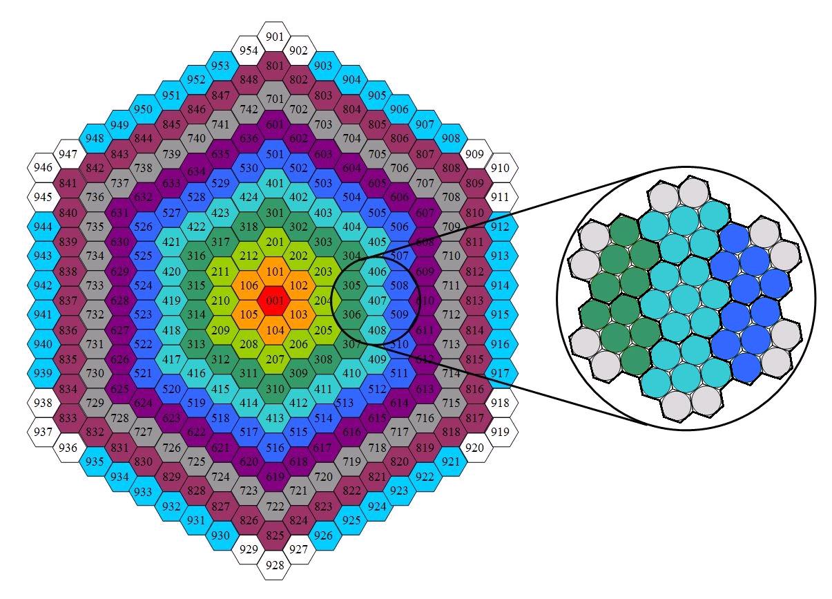
The computing power of low-cost FPGAs, the number of allowed input/output (I/O) channels and the speed of the links between PMTs and FPGA must be balanced with the size and the required overlap of camera regions. Some CTA camera designs define a group of 7 pixels (one central pixel and the six surrounding pixels) as basic building block that can be handled and exchanged independently of other pixels in a camera. Besides the PMT pixels such a so-called cluster contains also the needed infrastructure (high and low voltages), front-end electronics (preamplifiers, data buffers), and trigger boards. Each cluster has six direct neighbours, and a complete CTA camera can be built up by combining some hundred clusters as illustrated in Fig. 1 for an MST camera with 1897 pixels in 271 clusters. An arrangement of seven clusters (49 pixels) is referred to as super-cluster and subtends an angle of O(), i.e. it covers a good fraction of even the largest shower images. One cluster FPGA is assigned to each cluster and can receive up to 7 L0 signals from each of the 6 surrounding clusters by means of fast serial links. At the same time up to 7 L0 signals can be transmitted to each of the 6 surrounding clusters. Every cluster FPGA is thus the central engine of a super-cluster. In the design described here, there are 8 LVDS input and 8 LVDS output connections between any two cluster FPGAs. Each cluster FGPA utilizes 7 inputs from the local cluster and 5 of the 7 inputs from each of the six neighbouring clusters, cf. the inset in Fig. 1, i.e. the presently implemented firmware exchanges only 5 L0 signals with the surrounding clusters. Every cluster FPGA has thus 37 inputs, except for clusters that are located at the camera boundary and have therefore fewer inputs. This mapping allows the execution of trigger algorithms on the central 37 pixels of a super-cluster and creates a sufficient overlap of the super-clusters. The unused fast LVDS channels per connection extend the flexibility of the firmware design. They can be used to distribute other signals (like the camera trigger signal or a pulse per second (PPS)), across the camera backplane in a daisy chain way.
Due to the overlap of super-clusters a trigger condition can be found by more than one cluster FPGA. The detected trigger (the L1 signal) is therefore forwarded from all cluster FPGAs to a central FPGA. This FPGA can execute higher-level algorithms or even estimate image parameters. In the simplest case, it can derive a main trigger by just performing a logical OR on the triggers delivered by the cluster FPGAs. It can also interact with the camera data acquisition system to guide the camera readout since it has superior knowledge of the time development of the camera image possibly covering several super-clusters.
2.4 Hardware Implementation
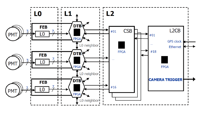
Hardware implementations of digital trigger components have been manufactured as a proof of principle for the concept using Altera444http://www.altera.com and Xilinx555http://www.xilinx.com FPGAs. In the following, a solution that encodes the TOT in the L0 signal length and that is based on the Xilinx Spartan 6 FPGA will be described in more detail. Figure 2 provides an overview of the different hardware components that are needed to generate and process the L0, L1 and L2 signals in a setup with only three 7-pixel clusters.
The implementation assumes that the L0 signals for seven PMTs are generated on the front-end board (FEB) that provides the basic infrastructure (voltage supplies, preamplifiers, data buffers) for a cluster. On the FEB, the PMT signals are preamplified and passed to a fast Low Voltage Differential Signaling (LVDS) comparator which compares the analogue signal with the signal at a second input whose signal level can be adjusted with the help of a digital-to-analogue converter (DAC) and that functions as a threshold. If the PMT signal exceeds the threshold, a digital LVDS L0 signal is created whose pulse length corresponds to the TOT of the PMT signal. The minimum detectable input pulse width is about 1 ns full width half maximum (FWHM), the minimum amplitude is about 0.3 photoelectrons.
A so called digital trigger backplane (DTB) board is mounted behind each cluster. The central element of the DTB board is the cluster FPGA receiving the L0 signals from its FEB. The FPGA exchanges L0 signals (L0 neighbour) with up to six neighbouring DTB boards by means of fast serial links and executes a trigger algorithm on the 37 channels assigned to it to generate a L1 trigger signal for its super-cluster. The generated L1 trigger signal comprises 2 bits, encodes the trigger type, and is typically propagated to the FPGA of a so-called cluster service board (CSB).
The hardware design for the L2 stage foresees a single electronics crate that fits easily into the body of a Cherenkov camera and can service up to 2016 pixels. The crate will house one L2 Controller Board (L2CB) and 18 CSBs. Each CSB accepts up to 16 L1 signals and processes them with the help of a single FPGA. In the simplest case, the CSB produces an OR of the 16 L1 signals and the resulting L1CSB signal is forwarded to a FPGA on the L2CB which is generating the L2 camera trigger signal from the 18 L1CSB signals.
2.5 FPGA Firmware Design
FPGAs operate synchronously (i.e. driven by one or several clocks) or asynchronously. Although FPGAs are optimized to run synchronously it is possible to implement a simple trigger (e.g. a coincidence of three neighbouring pixels, three next neighbours (3NN)) asynchronously in a purely combinatorial way. A first revision of the DTB board had been equipped with an Altera Cyclone IV FPGA. The Altera development system Quartus allows the very accurate constraining of the internal delays. A firmware design implementing a combinatorial 3NN condition for 49 pixels showed excellent results. An minimal L0 signal overlap of 1 ns was sufficient to generate an L1 trigger signal.
To enable more complex trigger algorithms that require pipelining the FPGA has to be used in a synchronous way. When comparing low-cost FPGAs, the Xilinx Spartan 6 FPGA has been preferred over Altera’s Cyclone IV for two reasons. Firstly, any input pin is equipped with an in-system-programmable delay line for delay adjustments of up to 10 ns in steps of roughly 40 ps allowing the finetuning of individual pixel delays. Secondly, each pin is equipped with so-called input and output serializer/deserializer stages (iSerDes and oSerDes). An iSerDes stage converts a serial bit stream of up to 950 million samples per second (MS/s) into parallel words that can be up to 8 bit wide. The word rate is then the serial bit rate divided by the word width, e.g. 800 MS/s at a word width of 8 results in a system clock of 100 MHz. An oSerDes stage performs the reverse operation and converts parallel to serial.
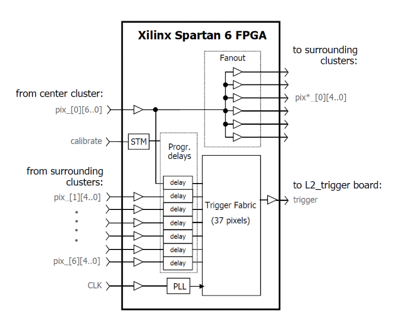
The second revision of the DTB board described here is based on a Xilinx FPGA of the Spartan 6 family. Figure 3 gives an overview of the basic FPGA building blocks (referred to in italics in this paragraph) and its inputs and outputs. The 7 L0 signals from the corresponding cluster are passed on to six neighbouring clusters via fanouts and low-cost flat band cables. They are also fed into a 37-pixel Trigger Fabric which receives the 30 L0 signals from the 6 neighbouring clusters. On all I/O channels for L0 signals, Programmable delays are used to compensate time differences between the channels. At the inputs of the Trigger Fabric, the iSerDes stages sample the L0 signals with a rate of 950 MS/s. With a SerDes factor of 8 this results in 8 time slices each of which 1.05 ns long. It is this sampling of the L0 signals that provides 1-bit camera images at a rate of about 1 GHz. The Trigger Fabric comprises, in fact, eight identical trigger fabrics that work in parallel. Each of the eight trigger fabrics is connected to one time slice and has 37 input bits. The 8-bit trigger word resulting from the processing of the trigger fabrics is connected to an 8-bit oSerDes stage and provides a single serial trigger signal with a fixed latency. Due to the sampling of the L0 signals the latency fluctuates by about ns. By moving the 8-bit words into shift registers the history of the L0 signals can be stored and thus be made available for trigger alghorithms based on the time distribution of individual pixel signals.
3 Trigger Prototype Boards and Tests
Hardware implementations of the L0 and L1 stages were developed and studied in detail in the laboratory in order to show the validity and stability of the hardware concept. The development work was accompanied by extensive software tests using a VHDL Test Bench and the Xilinx ISE v13.4 software for design implementation and simulation. Particular attention has been paid to the accuracy of timing simulations the results of which have been verified by a comparison of FPGA signals (e.g. trigger patterns) using an oscilloscope.
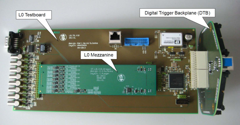
Figure 4 (top) shows a test setup where a dedicated L0 testboard provided the functionality that will come from the FEB in a real setup. In the following, the L0 testboard will also be referred to as FEB.

3.1 The L0 Mezzanine Board
The L0 signals are generated on a mezzanine board (Fig. 4, bottom) that is mounted on the FEB. This piggy back solution is just temporary; in its final implementation, the L0 stage will be directly soldered onto the FEB. The L0 mezzanine board is supplied with 3.3 V by the FEB. Linear regulators generate the 2.5 V voltage supply for the seven analogue input stages. They comprise a low-noise, low-offset amplifier and a fast comparator. The amplifier, adjusted to a gain of 5, converts the analogue signal from differential to single ended and provides in combination with the preamplifier on the FEB a signal of 13 mV/p.e. at the positive input of the comparator circuit. The negative input is driven by one output of an eight-channel DAC. The 8-bit DAC is controlled by the FEB FPGA via an SPI bus and provides L0 thresholds between 0 and 256 mV.
3.2 The Digital Trigger Backplane Board
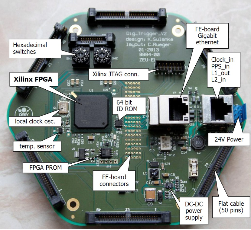
The DTB board is a hexagon-shaped 8-layer printed circuit board (PCB) that is 125 mm wide. An overview of its basic components (referred to in italics in the next paragraphs) is shown in Fig. 5. The processing of the 37 L0 input signals is done by a low-cost Xilinx FPGA of the Spartan 6 family of type XC6SLX252FGG484C. Other parts, worth mentioning, are a DC-DC power supply, a local clock oscillator, two rotating hexadecimal switches, a 64-bit ID ROM and a temperature sensor.
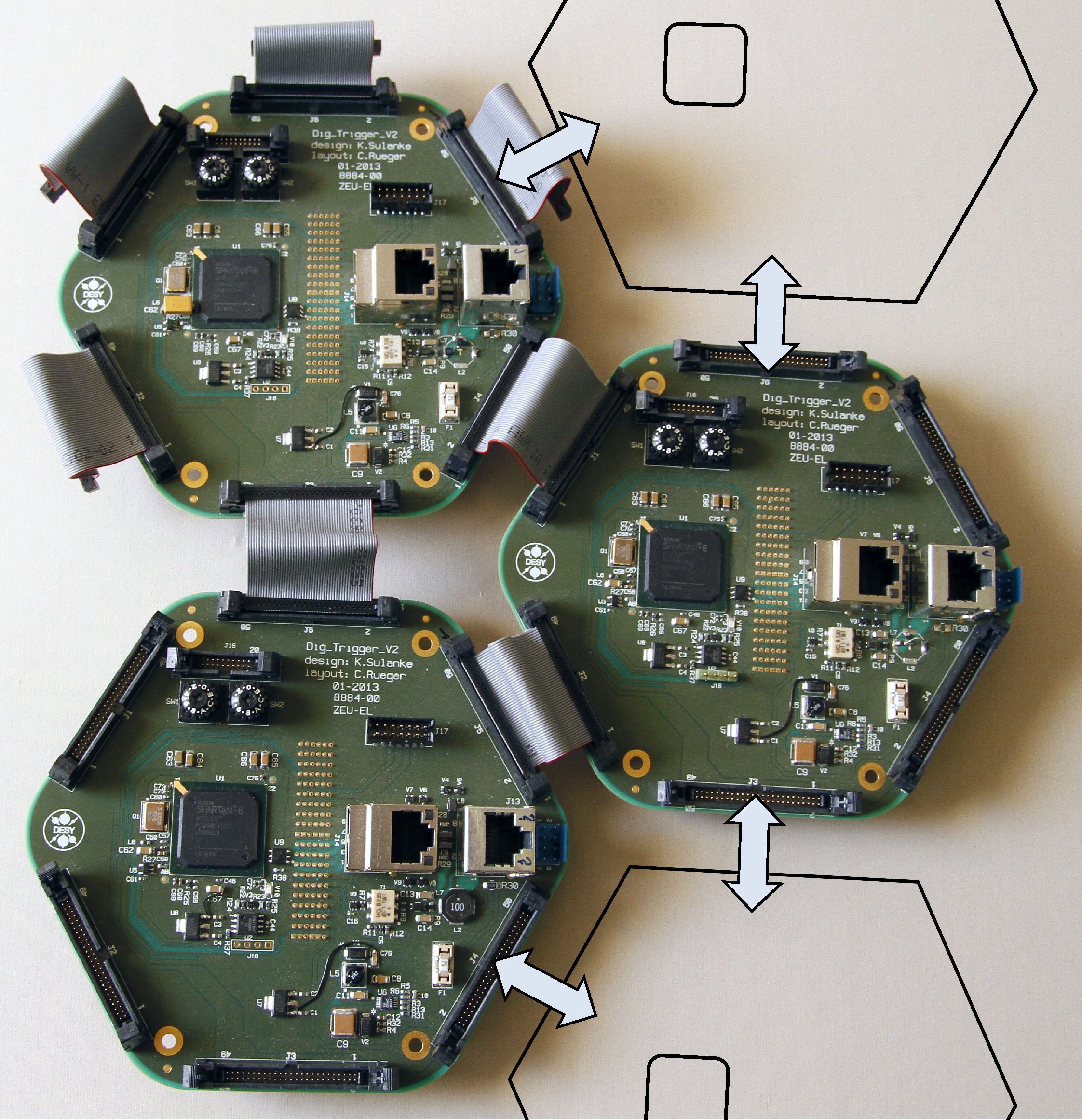
The seven L0 signals from the central cluster are received from the FEB FPGA through the FE-board connectors. The remaining 30 L0 signals are connected to the Xilinx FPGA using six peripheral 50-pin Flat cable connections to the neighbouring clusters (cf. Fig. 6). The same connections are used to fan-out the seven L0 signals from the central cluster. After power on, the FPGA gets automatically configured by a standard PROM. The PROM image can be altered either with the help of an onboard Joint Test Action Group (JTAG) connector and a programming cable, or by software from the FPGA on the FEB (exploiting the FEB’s ethernet connection). The DC-DC power supply circuitry generates the 3 V voltage needed by the two PROMs. Linear regulators driven by the 3 V are generating the FPGA’s power supply, 2.5 V and 1.2 V. A local clock oscillator is connected to the FPGA. The latter can also be driven by an external clock. An RJ45 connector is available for the transfer of trigger signals (L1_out, L2_in) and for synchronization by means of clock signals (Clock_in) and/or 1 Hz-pulses (PPS_in). At the same time this connector can also be used for the 24 V power connection. The two FE-board connectors (in the centre of the lower half of Fig. 5) establish the signal, power and FE-board Gigabit ethernet connection. Two general purpose rotating hexadecimal switches are useful to provide the FPGA with an input representing, e.g., the cluster position in the camera. Additionally, each of the six peripheral 50-pin flat cable connections has a signal pair for automatic neighbour detection. In this way the same firmware can be used, independent of the cluster position. The 64 bit ID ROM assigns a unique ethernet address to the FEB. The temperature sensor may be used to compensate for temperature-dependent L0 delay variations.
3.3 The L2 Crate
The L2 crate with its backplane and its components, the 18 CSBs and one L2CB, are still in the development phase. The anticipated size and weight are about 50x20x20 and roughly 11 kg, respectively. All boards are powered by the 24 V that are also used for supplying the 7-pixel clusters.
3.4 The Cluster Service Board
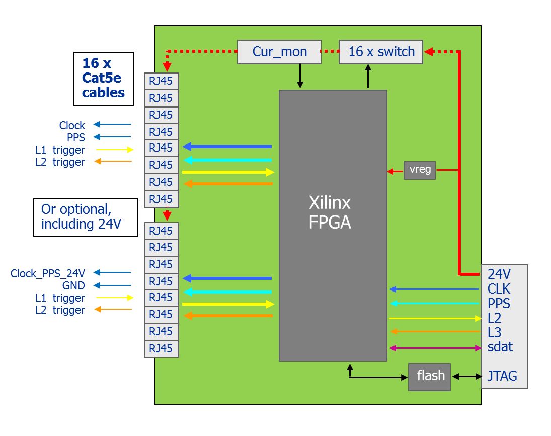
The CSB (see Fig. 7) is still in the design phase. It is based on a low-cost Xilinx FPGA that should combine arriving L1 signals into a logical OR. On the panel side of the CSB, there are 16 RJ45 connectors, one per cluster, used for distributing a global clock, a PPS and the camera trigger signal. The L1 trigger signal gets collected via this channel as well. Optionally, the 24 V power for the cluster can be distributed using the same cable. The board, about 18x16 cm2 in size, has at its back side a direct connector for plugging into the backplane of the L2 crate.
3.5 The L2 Controller Board
The L2CB has two interfaces, one pointing outside (away from the camera), the other pointing to the inside, establishing the connection to the CSBs. The outside interface comprises an Ethernet port and a connection to a central timing unit. The Ethernet connection is used to gather slow control information (e.g. cluster power consumption), for cluster-power switching and for configuring the trigger. Event-number driven time stamps could be transferred via this channel as well. The interface to a timing unit is the connection to a central clock/PPS source. The inside connection, the backplane of the L2 crate, carries the clock/PPS signals and the camera trigger. Additionally, there is a bidirectional serial communication channel to each CSB for exchanging slow control data and trigger configuration data.
3.6 Hardware Tests
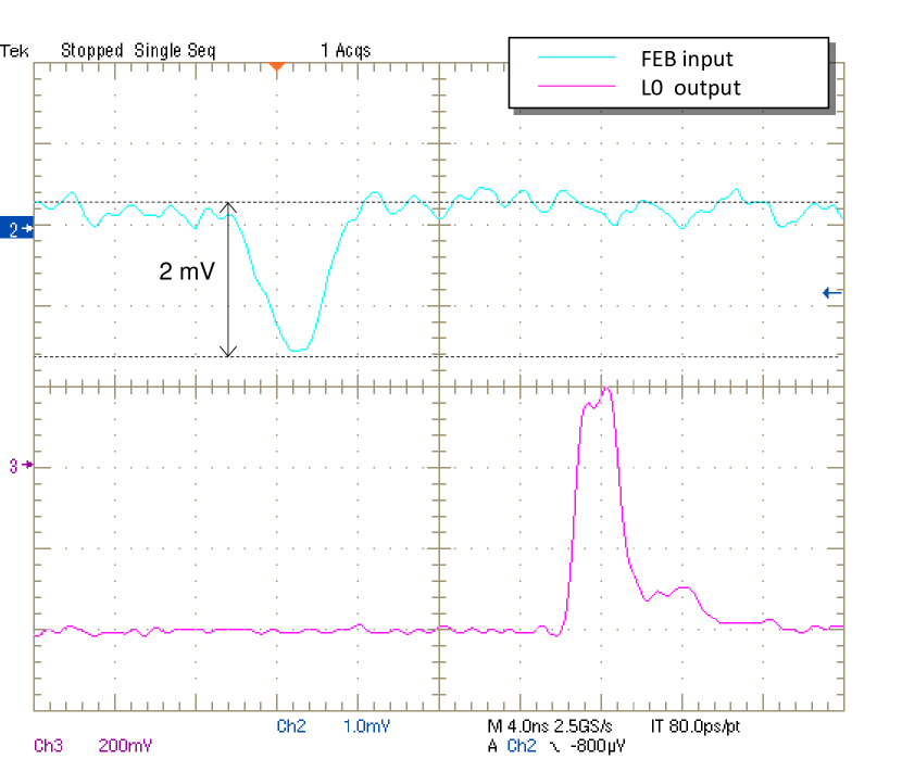
A number of trigger tests have been carried out using the hardware test bench described above. The L0 mezzanine board was tested by applying generator-driven pulses to the analogue inputs of the FEB. The analogue input signal passed an attenuator creating signal amplitudes as low as 1 mV. The DAC settings (between 0 and 256 mV) for the adjustment of the discrimination threshold were controlled by the FEB FPGA via a RS232 (or RS485) interface. With the selected settings (preamplifier gain adjusted to 5) signals with amplitudes down to 2 mV that correspond to 1 p.e. were securely detectable (as shown in Fig. 8). Channel-to-channel skews were found to be smaller than 50 ps; a suppression of more than 55 dB was measured for the amplitude of analogue crosstalk signals for neighbouring channels.
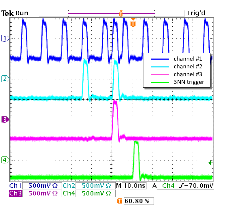
An efficient way to test the L1 stage, the DTB, is the connection of two DTB boards. In this setup, one board acts as pattern generator, while the second board functions as trigger board. The pattern generator, simply a particular firmware version, is based on a look-up table of 38 bit x 8k (up to 37k). 37 bits were used to emulate the 37 L0 signals, while the 38th bit decoded the expected outcome of the trigger. Figure 9 shows an example of such a test with a first revision of the DTB boards (equipped with Altera Cyclone IV FPGAs). The first three curves (blue and magenta) correspond to the L0 signals on three neighbouring channels and one sees the generated L1 signal (green) that occurred when the FPGA had been programmed to accept coincidences of three neighbouring channels (three next neighbours, 3NN) in an asynchronous firmware design.
3.7 Power Consumption and Price
For completeness, estimates of the power consumption and the price of the digital trigger are included here. Both power consumption and price are dominated by the DTB boards; the estimated power consumption for the L2 crate is 50 W.
A cost estimate of the various components on a DTB board can be found in Tab. 1. The listed prices are based on the assumption that more than 1000 DTB boards will pro produced. The estimated price per pixel is 19 €, which is about 12 % of the targeted channel cost (150–160 €). The power consumption of the DTB board is dominated by the FPGA which uses between 1.5 and 2 W depending on the complexity of the executed trigger algorithm. The generation of the L0 signals takes about 0.2 W per pixel, so the overall power consumption is between 0.4 W and 0.5 W per pixel. This power consumption is quite similar to the overall power consumption of analogue camera trigger designs [12].
| component | price |
|---|---|
| trigger PCB | 46 € |
| FPGA | 17 € |
| connectors and cabling | 50 € |
| board assembly | 20 € |
| total | 133 € |
| total, per pixel | 19 € |
4 Simulated Performance
In parallel to the design and test of trigger hardware, the performance of FPGA-based camera trigger algorithms has been investigated with the help of Monte Carlo simulations. A full comparison of the investigated trigger algorithms, the dependence of their performance on the NSB level, the telescope type, and the bandwidth of the used electronics are beyond the scope of this paper and are the subject of earlier ([13, 14]) and present work. The simulation results presented in the following are restricted to the case of Davies-Cotton type MSTs with a mirror area 100 m2 and a focal length of 15.6 m that are equipped with 1765-pixel PMT cameras [2] with a high-bandwidth front-end electronics and an FPGA-based trigger operating in asynchronous mode. The actual simulation of digital camera trigger algorithms followed closely the capabilities of a design (cf. Sec. 2.5) based on Altera FPGAs operated at 300 MHz in asynchronous mode. The conducted Monte Carlo studies had two objectives, namely (i) to show the importance of selecting a proper camera trigger algorithm and (ii) to illustrate how the combination of different trigger algorithms (which is easily possible with the FPGA-based trigger described here, but impossible with hard-wired trigger schemes) can improve the performance of a camera trigger. For simplicity and in contrast to the detailed design presented in Section 2 the simulation assumed that the FPGAs have access to all 49 pixels of a super-cluster (and not only to 37 pixels). Given the high degree of overlap between super-clusters the differences between the 49-pixel version and the 37-pixel version should be small.
4.1 Camera Trigger Simulations
| parameter | value |
|---|---|
| PMT signal shape | Gaussian (FWHM=2.6 ns) |
| PMT jitter | 1.5 ns (FWHM) |
| PMT excess noise factor | 1.175 |
| PMT after-pulse probability | 0.02 % |
| NSB level | 104–467 MHz |
The simulations of various camera trigger algorithms were performed with the trigsim software package (see [13] and A). Simulated air showers from protons and -rays at a zenith angle of were processed with the CTA detector simulation program sim_telarray [15] that provides the arrival times of shower-induced photoelectrons in the cameras of the Cherenkov telescopes. These photoelectrons were then injected into trigsim in order to carefully examine various trigger algorithms and readout options.
In the trigsim simulation, the time development of the PMT signal in every camera pixel was simulated in a window of up to 200 ns length with a time resolution of ns. The signal shaping implied by the PMT and the associated electronics was applied to each single p.e. and the shaped p.e. pulses were summed to obtain the full signal. Table 2 summarizes the signal shaping (a Gaussian with a FWHM of 2.6 ns) and the NSB rates that were used for this study. Photosensor after-pulses were simulated at the level of 0.02 % above 4 photoelectrons. The resulting ’analogue camera image’ for an event was then subjected to a number of different analogue and digital trigger algorithms in time and space. This procedure enables a strict unbiased comparison since statistical fluctuations in the analogue camera images impact all trigger algorithms in the same way.
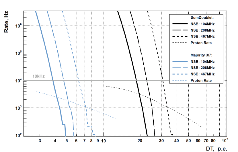
To determine accidental trigger rates due to the NSB-induced pulses and their after-pulses the response of the camera to continuous light with various intensities was simulated. Figure 10 shows the accidental trigger rate of an MST camera for NSB levels of 104 MHz (solid), 208 MHz (long dashes), and 467 MHz (short dashes) that roughly correspond to the observational conditions expected for CTA. The two lower NSB levels refer to observations of average extra-galactic and galactic field of views; the highest NSB level (4.5 times the extra-galactic NSB) stands for extreme observation conditions (e.g. during moonshine). The rates are shown as function of the discriminator threshold value (labelled ”DT”), calibrated in units of photoelectrons collected at the last PMT dynode. Different camera trigger algorithms (detailed below) are shown in black and blue, respectively. For each algorithm the trigger threshold DT was chosen such that an accidental camera trigger rate of 10 kHz occured. With this setting, the collection area for -rays is a simple figure of merit for the different camera trigger algorithms.
4.2 Camera Trigger Algorithms
One analogue and several digital camera trigger algorithms have been studied in detail in order to explore a variety of options. The parameters of all algorithms (e.g. coincidence windows, clipping levels) were optimized to obtain the best performance at a given NSB suppression. An analogue sum trigger is not possible with the hardware described above but is generally considered as the most suitable solution for the LSTs operating at the lower end of the CTA energy range. The simulation of an analogue sum trigger was therefore included as a reference trigger:
- SumDoublet
-
The simulated analogue sum trigger is based on overlapping trigger patches that comprise 14 pixels in two neighbouring 7-pixel clusters. Such a trigger patch is referred to as doublet and there are 12 overlapping doublets in a super cluster (cf. the inset in Fig. 1). Pulses were clipped at the level of 7.5 p.e. and the threshold of the trigger patches was 18 p.e. (for the default NSB level of 104 MHz).
In the simulation of digital camera trigger algorithms executed on an FPGA in asynchronous mode, the minimum overlap of the L0 signals that is required to produce a logical AND in an FPGA was set to ns. The coincidence window is then defined by and the length of the L0 signal. The effective coincidence window was optimized by varying the L0 signal length in steps of 3.3 ns. The explored algorithms were:
- Majority 3/7
-
This digital majority trigger required out of the 7 pixels in a trigger patch to be above the pixel threshold DT. The trigger patches were defined around those 25 pixels in a super cluster that are not located at the super cluster boundary (cf. the inset in Fig. 1); the trigger patch comprised the central pixel and its six neighbouring pixels. The L0 signal length was 3.3 ns and a coincidence of all pixels was required. The pixel threshold was 3.8 p.e. at 104 MHz.
- Majority 4/7
-
Like Majority 3/7 but with and correspondingly lower pixel threshold.
- Binary Trigger: 3/7 or 4/7
-
This algorithm is the logical OR of refined versions of the Majority 3/7 and Majority 4/7 algorithms that were assumed to be executed in parallel in the FPGA trigger fabrics. The L0 signal length was 3.3 ns. Each of the majority triggers had an independent pixel threshold (4.0 and 3.6 p.e. at 104 MHz, respectively) and a coincidence was only required for neighbouring pixels (and not for all pixels like in the case of the Majority 3/7 and Majority 4/7 triggers). Only coincidences occurring in a time window of less than 25 ns contributed to the trigger.
- Majority 5/21
-
This majority trigger required pixels above a threshold of 3.0 p.e. at 104 MHz in a trigger patch comprising three clusters (21 pixels). The trigger patches comprised the central cluster of a super cluster and two clusters at the super cluster boundary that are adjacent to each other. There are six such overlapping trigger patches. The L0 signal length was 6.6 ns.
- Majority 7/21
-
Like Majority 5/21 but with , a lower pixel threshold (2.8 p.e. at 104 MHz), and an L0 signal length of 9.9 ns.
It is noted here that an actual implementation of the Binary Trigger would require two comparators for L0 signals above independent pixel thresholds. This feature is not present in the prototype hardware described in Section 3 but could be added in a future version.
4.3 Comparison of Camera Trigger Algorithms
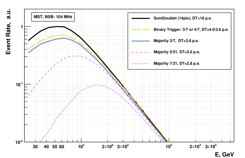
Figure 11 shows the normalized trigger rates of the discussed camera trigger algorithms as a function of the simulated -ray energy. The simulated NSB level was 104 MHz and the NSB-induced camera trigger rate was fixed to 10 kHz. The trigger rates have been calculated for a -ray source with a photon index of 2.45. The energy threshold of each algorithm (defined as the energy where the maximum trigger rate occurs) was estimated with a typical error of 5 %. All rates have been normalized such that the rate assumes a value of unity at the threshold of the SumDoublet trigger (black solid line).
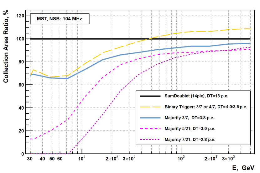
In in a similar way, the relative -ray collection area as a function of simulated -ray energy is depicted in Fig. 12 for the same simulation settings. All curves have been normalised to the SumDoublet trigger the good performance of which has been used as a reference. It is evident from Figs. 11 and 12 that the analogue SumDoublet trigger (black lines) provides the lowest threshold (55 GeV) and the largest collection area below 500 GeV making it the algorithm of choice for telescopes operating at the lower end of the CTA energy range. The Majority 5/21 and Majority 7/21 triggers (magenta, short-dashed curves) have poor performance for low photon energies since the 21-pixel trigger patches require a rather high pixel multiplicity ( or 7) to keep the NSB rate under control. At such high pixel multiplicities, many small -ray shower images will not trigger the camera. The resulting thresholds are 90 GeV and 150 GeV for the Majority 5/21 and Majority 7/21 algorithms, respectively. The Majority 3/7 trigger (blue curves) performs better than a Majority 4/7 trigger (not shown in Figs. 11 and 12) and was found to be the best choice among all simple majority triggers. Its threshold is 70 GeV and its collection area for photons at the typical MST threshold of about 100 GeV is only 30 % lower than for the SumDoublet trigger; this difference diminishes to 10 % at energies greater than 1 TeV. The Binary Trigger: 3/7 or 4/7 (long-dashed, yellow), if implemented, would have the same threshold but would be more performant than the simple Majority 3/7 trigger at all energies. In the simulation, their collection areas below the MST threshold are comparable but still 30 % lower than the collection area obtained with an analogue sum trigger. The effective area of the binary trigger converges, however, quicker towards the collection area of the SumDoublet trigger and surpasses its performance at energies greater than 500 GeV. The binary trigger also accepts high-energy showers with large impact parameters and hence sizable time gradients since a coincidence in time is only required for adjacent pixels. Overall, the performance of the binary trigger demonstrates clearly how the paralled execution of trigger algorithms with the help of low-cost FPGAs can help to exceed the performance of other approaches.
5 Summary
The presented design of an FPGA-based digital trigger allows the triggering of cameras with an estimated latency between 80–300 ns, depending on complexity of the executed algorithm. The design grants the trigger algorithms access to overlapping camera regions that are large enough to contain a sizable fraction of a typical shower image. Each trigger algorithm can exploit the information for 37 pixels in its region in the space and time domain. Several trigger algorithms can be executed in parallel, and their results can be combined to result in a more informed trigger decision. This allows, for example, the deployment of different algorithms that are focussed on the lowest and highest -ray energies, respectively, and whose results can be combined to obtain a superior performance over the full energy range. Thanks to the use of re-programmable FPGAs, an update of the trigger algorithms is quickly possible, thus the most suitable algorithm for certain observation conditions and the targeted -ray source can be chosen. In addition to the execution of trigger algorithms the FPGAs could provide input for the acquisition and online reduction of the pixel data (adjustment of the readout window in time, zero suppression). This flexibility and extensibility are inherent features of this trigger design and come at no extra effort.
The functioning of the produced prototype boards and the successful tests of the different trigger stages suggest that the digital camera trigger is viable option for Cherenkov cameras in CTA. The power consumption and the estimated price per channel are well within budget of a Cherenkov camera.
6 Acknowledgements
The authors would like to thank the members of the CTA consortium for stimulating discussions. We are grateful to the anonymous referee whose comments helped to improve the manuscript. Konrad Bernlöhr is acknowledged for help with the CTA simulation tools and for comments on Sec. 4. We also would like to thank Oscar Blanch Bigas for his valuable contributions to trigsim.
Appendix A The trigsim Simulation
The trigsim software package was developed within the Monte Carlo simulation effort for CTA in order to quickly explore the large variety of camera trigger algorithms and their parameters. It is available on request from the authors666Contact U. Schwanke (schwanke@physik.hu-berlin.de) and consists of a library (written in C++) and a main program that is also called trigsim. The package depends on two external software packages, namely root [17] and hessio. The hessio package implements the platform-independent eventio [15] format that is used to store the output of CTA detector simulations in files.
The input to trigsim are eventio files with the output of the detector simulation program sim_telarray [15] that simulates the response of CTA candidate arrays to the Cherenkov light emitted by air showers initiated by photons, electrons and hadrons. The input files contain the geometry of the detector (arrangement of telescopes, camera geometry), the simulated particles (type, energy, direction), and for each camera pixel in a telescope the times when single photoelectrons were created at the PMT cathode777Storage of photoelectrons is enabled by setting SAVE_PHOTONS=2 in sim_telarray. trigsim copies the detector geometry from the input files and can not, of course, change the PMT efficiency a posteriori, but all other aspects of the signal processing (NSB rates, PMT jitter, signal shaping, digitization etc.) can be changed under the control of configuration files and command line arguments. For most applications trigsim loops over the events in the input files, but it can also be steered to disregard the p.e. information and to just simulate the response to NSB photons that are created internally. In the latter case, the input files solely serve to extract the detector geometry. The simulation output of trigsim is typically stored in root files that can be directly analysed or fed into a shower reconstruction program. For debugging and cross-checks trigsim allows the creation of graphical displays of camera images and of simulated signals; it is also possible to inspect individual events while the program waits for a keyboard input.
The central engine of trigsim is a base class (Trigger::TriggerBase) defining a set of virtual member functions that accept data blocks as arguments (containing, for example, the detector geometry or the photoelectrons for a single shower) and which are called by the trigsim main program when reading Monte Carlo input files. For a typical simulation study one has to subclass the base class (or one of the already existing derived classes), overwrite the virtual functions as desired, and modify a static function that returns an instance of the new class to the trigsim main program; there is no need to modify the main program and one can switch from one simulation study to another by passing a command line argument to trigsim.
References
- [1] Acharya, B. S. et al. [CTA Consortium], Astroparticle Physics 43 (2013) 3.
- [2] Bernlöhr, K. et al. [CTA Consortium], Astroparticle Physics 43 (2013) 171.
- [3] Heß, M. et al. [HEGRA Collaboration], Astroparticle Physics 11 (1999) 363.
- [4] Funk, S. et al., Astroparticle Physics 22 (2004) 285.
- [5] Hermann, G. et al., American Institute of Physics Conference Series 1085 (2008) 898.
- [6] Schroedter, M. et al., arXiv:0908.0179, 2009.
- [7] Naumann, C. L. et al., Journal of Instrumentation 8 (2013) P06011.
- [8] Meucci, M. et al., Nuclear Instruments and Methods in Physics Research A 518 (2004) 554.
- [9] Zitzer, B. for the VERITAS Collaboration, Proceedings of the International Cosmic Ray Conference 2013 Rio de Janeiro, arXiv:1307.8360, 2013.
- [10] Vincent, P. et al. [H.E.S.S. Collaboration], International Cosmic Ray Conference 5 (2003) 2887.
- [11] Aliu, E. et al. [MAGIC Collaboration], Science 322 (2000) 1221.
- [12] Barcelo, M. et al. for the CTA Consortium, arXiv:1307.3169, 2013.
- [13] Wischnewski, R., Schwanke, U., Shayduk, M. and Sulanke, K. for the CTA Consortium, Proceedings of the International Cosmic Ray Conference 2011, Beijing, vol. 9, p. 63, arXiv:1111.2183.
- [14] Shayduk, M., Vorobiov, S., Schwanke, U. and Wischnewski, R. for the CTA Consortium, Proceedings of the International Cosmic Ray Conference 2013, Rio de Janeiro, arXiv:1307.2232, 2013.
- [15] Bernlöhr, K. Astroparticle Physics 30 (2008) 149.
- [16] https://www.hamamatsu.com/resources/pdf/etd/PMT_handbook_v3aE.pdf
- [17] Brun, R. and Rademakers, F. Nuclear Instruments and Methods in Physics Research A 389, (1997) 81.