Contact doping, Klein tunneling, and asymmetry of shot noise in suspended graphene
Abstract
The inherent asymmetry of the electric transport in graphene is attributed to Klein tunneling across barriers defined by pn-interfaces between positively and negatively charged regions. By combining conductance and shot noise experiments we determine the main characteristics of the tunneling barrier (height and slope) in a high-quality suspended sample with Au/Cr/Au contacts. We observe an asymmetric resistance across the Dirac point of the suspended graphene at carrier density cm-2, while the Fano factor displays a non-monotonic asymmetry in the range . Our findings agree with analytical calculations based on the Dirac equation with a trapezoidal barrier. Comparison between the model and the data yields the barrier height for tunneling, an estimate of the thickness of the pn-interface nm, and the contact region doping corresponding to a Fermi level offset of meV. The strength of pinning of the Fermi level under the metallic contact is characterized in terms of the contact capacitance F/cm2. Additionally, we show that the gate voltage corresponding to the Dirac point is given by the work function difference between the backgate material and graphene.
I Introduction
Klein tunneling is one of the most spectacular effects of relativistic quantum field theory described by the Dirac equation. This tunneling phenomenon, present even in the regime of impenetrable barriers, leads to peculiar transport properties of graphene. Klein tunneling is the backbone of transport due to evanescent modes causing the observed pseudodiffusive behavior of ballistic graphene samples Tworzydlo et al. (2006); Katsnelson et al. (2006). The bimodal distribution of transmission eigenvalues in ballistic graphene coincides with a diffusive conductor, which results in shot noise non-distinguishable from diffusive mesoscopic conductors. Furthermore, the evanescent modes lead to a minimum conductivity of in the ballistic regime Katsnelson (2006). Evidence of these Klein tunneling phenomena have been obtained from observations of charge transport and shot noise in a graphene sheet with ballistic characteristics Miao et al. (2007); Danneau et al. (2008a); Du et al. (2008).
The most commonly employed assumption in the analysis of the conductance and shot noise of ballistic graphene has been to consider the carbon layer underneath the electrodes as strongly doped, and this can be modelled using a rectangular electrostatic potential Katsnelson et al. (2006); Tworzydlo et al. (2006); Sonin (2008). In reality, this assumption suffers of severe limitations as in a real device the charge density varies continuously and the rate of change is governed by the screening length. Various theoretical models for finite-slope potentials have been analyzed for -interfaces in graphene Cheianov and Fal’ko (2006); Shytov et al. (2008); Cayssol et al. (2009). All the models have predicted asymmetry in transport properties with respect to the gate voltage, i.e. whether the charge carriers are electrons or holes. In recent experiments, such asymmetry has been observed Huard et al. (2007, 2008); Stander et al. (2009). In the ballistic regime, this asymmetry is attributed to the Klein tunneling Stander et al. (2009); Rickhaus et al. (2013); Oksanen et al. (2014) while scattering by charged impurities Novikov (2007); Chen et al. (2008) plays also a role in the diffusive regime. Furthermore, evidence of Klein tunneling has been reported in conductance experiments in confined geometries displaying phase-coherent and double-junction interference effects Young and Kim (2009, 2011). Sharp -interfaces have also been achieved in non-suspended samples using air-bridge type gates Liu et al. (2008); Gorbachev et al. (2008). A full understanding of contact issues is of vital importance for the development of novel electrical components using graphene and other 2-dimensional materials Ferrari (2014). In particular, detailed understanding of -interfaces is critical for optoelectronics components Tielrooij et al. (2015).
The asymptotic carrier transport in Klein tunneling is bound to be affected by the strong influence of the metal contacts on graphene. A simple contact model was formulated by Giovannetti et al. Giovannetti et al. (2008) who also performed DFT calculations concerning the involved work functions. In this paper, we generalize this model to include the effects of the applied backgate voltage, and we combine the resulting model with tunneling calculations based on the Dirac equation in order to obtain a comprehensive transport model for analyzing electrical conduction in a ballistic, suspended graphene sample. We employ a trapezoidal form for the tunneling barrier which we show how to treat analytically Sonin (2009). By using conductance and shot noise experiments performed on a high-quality suspended graphene sample, we can determine the barrier parameters and their relation to the doping of the graphene by a metallic contact. In comparison with DFT calculations Giovannetti et al. (2008), we find a semiquantitative agreement for the graphene-modified metal work functions as well as for the distance between the charge separation layers which govern the contact capacitance between the metal and graphene.
The experiment and the agreement with the theoretical model confirm the existence of Klein tunneling in graphene. Our method works well even in the situation in which the work functions of the contact metal and graphene differ by a relatively small amount (tens of meV). As such, our results suggests a novel method to find the work function of materials. Note that the work function difference between two metals is not measurable directly: the standard way for its determination is the use of Kelvin probe force microscopy, where the electrical capacitance between the metal and a probe is varied in order to induce a measurable AC current. Our results demonstrate that there exists a gating effect in the position of the Dirac point of the suspended graphene due to the work function of the backgate. Thus, by using a material as backgate for graphene and measuring the gate voltage corresponding to the Dirac point one can get a simple DC measurement of the work function.
The paper is organized as follows: after the present introduction as Sect. I, we present a complete theoretical treatment of the problem of gated suspended graphene with metallic contacts in Sect. II. The structure of our samples are detailed in Sect. III together with the employed methods for shot noise measurements. Our experimental results and their analysis are presented in Sect. IV. The implications of the results are discussed in Sect. V jointly with a comparison to other works.
II Theoretical background
II.1 Electrochemical model for suspended graphene samples
When a graphene sheet is brought in contact with a metal, electrons will flow between them in order to equilibrate the Fermi level. This effect has been analyzed in detail in Refs. Giovannetti et al., 2008 and Xia et al., 2011. We proceed beyond these works and introduce a complete electrochemical model for a suspended graphene sample with metallic contact electrodes. Our model takes into account consistently the effect of the backgate on the doping of the graphene under the metal. We show that this effect can be neglected only if the difference between the work function of the metallic contact electrode and the graphene layer is large enough (i.e. in the limit of high barrier, defined below Eq. (17)). If this is not the case, the contact-region doping acquired from the backgate voltage has to be included in the transport calculations. On top of the electrostatic contributions, our model indicates that the work function difference between the backgate and graphene enters the equilibrium charge density, which, in particular, leads to a small shift in the Dirac point of the suspended part of the graphene. Using electrochemical equilibrium conditions, we derive analytical equations that incorporate all these effects.
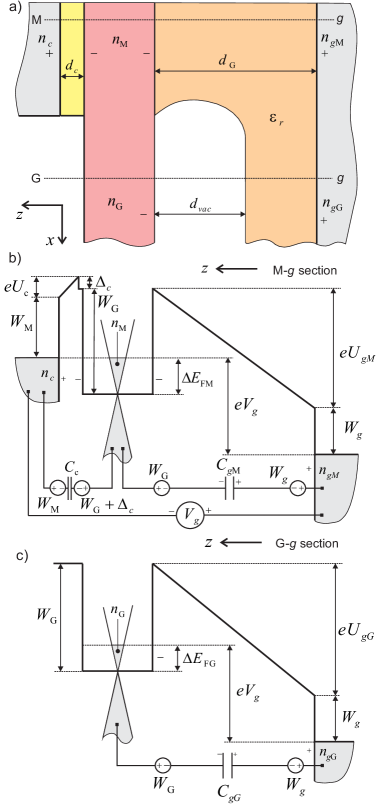
In Fig. 1 a) we present a schematic sideview of the sample, showing the region of contact with the metal and the graphene as well as the backgate. For clarity, we have exaggerated the size of some components, so the figure is not to scale. On the sample chip, the graphene sheet is placed at a distance of nm from the backgate. The sheet is supported by a SiO2 insulating layer (), which is partially etched away under the graphene. This results in a vacuum gap of height nm. Further details on the sample and the metallic contacts are found in Sect. III.
In our sample structure, the capacitance per unit area between the graphene and the backgate in the support region (graphene under the metal) is estimated from the regular parallel plate formula
| (1) |
which yields F/cm2 using the above mentioned values for and . In the suspended region, the graphene capacitance per unit area against the backgate can be calculated using the formula for two capacitors in series: a vacuum capacitor with a plate separation of and a capacitor with the spacing filled with dielectric material having . This results in the capacitance per unit area
| (2) |
In our calculations the actual value for the suspended part capacitance is taken from our Fabry-Pérot measurements F/cm2 Oksanen et al. (2014), which agrees well with the above theoretical value.
Next, we analyze the electrochemical potentials that appear in this experimental setting. We take two cuts through Fig. 1 a), one across the dashed line M-, and the other across the dashed line G-, and we represent the spatial variation of the electrochemical potential in Fig. 1 b) and Fig. 1 c), respectively. The work function of the pristine graphene is denoted by . At the contact with the metal, this work function may be modified by a small shift, see Ref. Giovannetti et al., 2008. The work function of the contact metal on top of the graphene is denoted by , while the work function of the backgate is . Note that according to Volta’s rule, the contact potential at the end of a circuit is determined only by the work functions of the circuit elements at the end; therefore no other work function, for example corresponding to various other metals along the measurement chain, can enter in this problem. The difference between the work function of the gate and that of graphene is denoted by : this quantity will turn out to be the shift of the Dirac point of the suspended region of graphene due to the backgate work function. Following the common practice in graphene research, gate voltages in the following formulas will be measured with respect to the Dirac point, with the corresponding shifts defined as
| (3) |
We first solve the problem of finding the surface charge distribution for the electrochemical potentials presented in Fig. 1 b). At the contact between the metal and the graphene, the electrons will move from the electrode with the lower work function into the electrode with the higher work function. As a result, a surface charge distribution will appear in the contact region, producing an electrostatic potential across the contact capacitance , the magnitude of which reflects the spatial variation of the surface charge. According to DFT calculations, F/cm2 Giovannetti et al. (2008). A relevant parameter for charge transfer between the metal and graphene is the difference between the work functions of the graphene under the metal and the work function of the metal, which is described by
| (4) |
where is the work function of the metallic contact material and denotes the modified work function of the graphene under the contact. Another electrostatic potential is established across the capacitance , with a surface charge on the gate. The total particle-number surface density in the graphene layer in the contact region is therefore
| (5) |
The first equilibrium condition is obtained from the condition that the difference between the Fermi level of the metal and that of the gate equals . This condition does not formally involve the characteristic density of states of graphene. Hence, as shown by the circuit schematics below the Fermi level diagram in Fig. 1 b), it can be regarded as a pure electrostatic condition. It states
| (6) |
The second equation governing the equilibrium involves the intrinsic properties of graphene, and it can be obtained by using the condition that the Fermi levels of the metal and the graphene under the metal coincide:
| (7) |
In the graphene under the metal, where the linear graphene bands are supposed to persist, the relation between the number of negatively-charged carriers per unit area and the shift in the Fermi level is given by
| (8) |
where m/s is the Fermi velocity. It is useful to introduce a constant relating the Fermi speed and the fundamental constants and :
| (9) |
We propose to call this quantity Fermi electric flux. This constant is related to the concept of quantum capacitance (for graphene, see Ref. Fang et al., 2007) and to the fine structure constant of graphene, as detailed in Appendix A. The Fermi electric flux determines the energy shifts produced by graphene as it is inserted in to an electrical circuit. For m/s, the equation yields Vcm.
Combining now Eqs. (5-8) above, and choosing the proper physical solution, we obtain the final result for the shift of the energy level of graphene under the metal,
| (10) |
An experimentally relevant limit for Eq. (10) is the case of a very large contact capacitance : if the material parameters are such that and the charge induced by the gate voltage is relatively small, then , and we obtain from Eq. (10). In this situation, the large contact capacitance locks the position of the Dirac point of the graphene under the metal to a value set by the parameter .
In our experimental setup, in fact, remains relatively small, which makes the quantity comparable with at large values of . Consequently, the Fermi level can even reach the Dirac point of the graphene under the metal . As the latter condition does require substantial gate voltages, we could not reach this regime in our experiment.
Next we turn to the suspended part of the graphene. In this region, the charge accumulated on the surface of the backgate , which produces a voltage drop , is exactly compensated by the charges on the graphene side having the particle-number surface density ,
| (11) |
Then, the condition that the electrochemical potential difference between the Fermi level of graphene and the Fermi level of the backgate is reads
| (12) |
where
| (13) |
in parallel to Eq. (8). From Eqs. (11-13), we find for the Fermi level shift in the suspended part:
| (14) |
Note that corresponds to , i.e. is indeed the Dirac point of the suspended graphene. For , typical experimental conditions fulfil , which allows one to approximate . This limit was assumed in the previous analysis by Sonin Sonin (2009).
The difference of the Fermi energies of the suspended graphene and the graphene under the contact results in an electrostatic potential difference between the free-standing region of graphene and the one under the metal:
| (15) |
This leads to a potential barrier for the electrons traveling along the -direction, from one metallic contact to the other, as detailed in the next subsection. Since transmission through the potential barrier is foremost sensitive to the slope of the barrier at the charge neutrality point, we have adopted a trapezoidal barrier shape where the slope is constant on both sides of the flat top of the barrier. This trapezoidal form is tractable using analytical calculations, and it is expected to catch the basic features of the tunneling transport problem.
II.2 Klein tunneling: conductance and Fano factor
The asymmetry in electrical transport across a basic, back-gated graphene device is related to many aspects of the sample, its quality, and biasing conditions. It depends on the nature of transport, whether it is ballistic or diffusive, on the presence of interfaces between p- and n-doped regions, on the steepness of the slopes of the electrostatic potential barrier, on the doping due to the contacts, and on the coherence of the transport between the reflecting interfaces (pn-type of interface or two unipolar regions with different doping, either p and p’ or n and n’, yielding pp’- and nn’-interfaces). The type of junction is determined by the sign of the Fermi level shifts: if and we have a junction at the left contact, if and we have a junction, if and we have a junction, and if and we have a junction. The same notions apply to the right contact provided that the regions are considered from right to left, instead of the left-to-right direction used for the left contact above.
Our experimental data deal with suspended graphene with a mean free path on the order of the sample length. Consequently, we will consider foremost Klein tunneling in the ballistic regime and neglect the influence of disorder Fogler et al. (2008). Unlike the early work discussed above, we take into account the weak doping of contact regions when using Au/Cr/Au leads. We assume symmetric contacts although in reality there is always slight asymmetry. In our context, this assumption means that the values of the work function difference are equal at both contacts. The asymmetry of the contact resistance can be neglected as the contact resistance is found to be insignificant in the analysis. The use of moderate voltages and cryogenic temperatures also guarantees negligible role of acoustic phonons Das Sarma et al. (2012).
Below, we derive the formulae for the transmission and reflection coefficients, as well as the conductance and Fano factor, for the tunneling geometry given in Fig. 2. The figure shows variation of the electrostatic potential (see Fig. 1) in the -direction along the whole graphene sheet including the end contacts. We consider only propagating modes; this approximation is justified by the criterion that propagation through the evanescent modes can be neglected if the bias voltages are clearly above Sonin (2008), where is the length of the sample. For a typical sample of length m, mV, well below the bias voltages used in our experiments for shot noise ( mV).
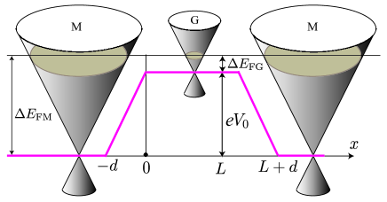
The use of the Dirac equation with a trapezoidal barrier is the simplest approximation for transport in a two-lead graphene sample with a pair of pn-interfaces due to spatially varying charge doping. The electrostatic trapezoidal barrier (of structure nn’n) in Fig. 2 is comprised of five distinct regions: the middle part , corresponding to the region G from the previous subsection, where there is a step in electrostatic potential (difference in the potential between the contact regions and the center), two sloped regions and in the vicinity of the graphene/metal interfaces, where the electric field is finite, and finally the contact area and with zero (or small bias) potential, corresponding to the region M of graphene fully covered by the contact metal. Dirac electrons propagating along the -direction may thus experience Klein tunneling under this barrier. In the left slope region , the potential is written in the form . The parameter sets the absolute value of the voltage slope. In general, the barrier can have either a positive or a negative slope, depending on the sign of . For clarity, we will give the explicit analytical forms of the solutions of the Dirac equation only for the case of positive slope, corresponding to the left side of the barrier in Fig. 2. The solutions for negative slope can be obtained by the same procedure.
All the energies are measured from the Dirac point of the graphene under the metal, with the standard convention that is positive if the Fermi level is above the Dirac point and negative otherwise, see Eqs. (8) and (10). A similar convention is used for , see Eq. (13-14).
The massless Dirac equation for a graphene sheet can be written as
| (16) |
where for particles near the Fermi level , and the upper and lower components of the spinor are denoted by and respectively. Note that the electrons at the Fermi level will have energy in any of the regions M, G, or in the slope region. We can solve the Dirac equation in Eq. (16) by the method of separation of variables, writing , with the current along the direction normalized to .
The height of the energy barrier defines a step in the momentum of the Dirac electrons as they cross the barrier. The influence of this change in momentum can be characterized compactly using a dimensionless parameter, the impact parameter, defined as
| (17) |
The impact parameter will play an essential role in our calculations below. Note that the earlier theoretical treatment by Sonin Sonin (2009) assumed a large impact parameter . As this approximation is not valid for our present experiment, a finite needs to be taken into account in the theory.
Assuming that the thickness of the sloped region is independent of the gate voltage, allows us to express the absolute value of the slope of the barrier in terms of the -dependent quantities, and , which yields
| (18) |
Likewise, we obtain for the impact parameter
| (19) |
Note that the impact parameter increases with the absolute value of the slope, as evident from Eqs. (17) and (18).
II.2.1 Top of the barrier, (region G)
In this region we consider an electron moving to the right, . The Dirac equation can be solved, with
| (20) |
for both positive and negative ,
| (21) |
where the sign denotes . The absolute value of the wavevector is
| (22) |
and . Note that remains unchanged over all region crossings.
II.2.2 Slope of the barrier,
In this region we have
| (23) |
depending on weather the slope is positive or negative. Here is the crossing point, defined as the position where the kernel is nullified, and it is given by . The solutions have been found by Sauter (see Ref. Sonin, 2009); for positive slope, with the substitution we have
Note also that the dimension of is [length]-2, while that of and is [length]-1; hence the quantity , that enters the hypergeometric functions, is adimensional.
The functions and are defined through the Kummer confluent hypergeometric function ,
| (24) |
and
| (25) |
From the boundary conditions at we obtain
| (26) | |||||
| (27) |
Importantly, a consequence of the normalization is the fact that and , which can be verified explicitly using the explicit expressions above.
II.2.3 Graphene under the metal (region M)
In the calculation of Sonin Sonin (2009), this region with was disregarded on the basis of the assumption ). It turns out that this condition is not valid in our experiment (cf. Fig. 5), and the behavior in the region has to be taken into account. In this region,
| (28) |
The absolute value of the total momentum at the Fermi level is then
| (29) |
The corresponding momentum in the x-direction equals to , and the wave is a superposition of a reflected and a transmitted component,
| (30) |
Here and are the reflection and transmission amplitudes, is the sign of , and in the last exponent is .
Note also that in Eq. (30) the reflected component is normalized to the current in the x-direction, equal to , while the transmitted component is normalized to . However, one can explicitly check that the overall normalization of is to , provided that . This ensures that the normalization is the same for all the three regions. To understand intuitively how this is realized, note that the admixture of the reflection component in of Eq. (30) is compensated by an increase in the component propagating to the right, since becomes subunitary.
By imposing the condition of continuity of the wave function at , after some algebra we obtain the complex transmission amplitude
| (31) | |||||
II.3 Conductance and Fano factor for the whole barrier
To calculate the total transmission through the barrier, we employ incoherent addition of the transmission coefficients. Usually phase coherence is more sensitive to disorder than reflection and transmission, and we address the case when the former is destroyed but the latter is not affected by disorder (ballistic regime). This assumption is supported by the experimental fact that the Fabry-Pérot resonances are found to be weak. Furthermore, when destroying the Fabry-Pérot resonances fully by an applied bias, the overall conductance does not change much. Hence, we consider the incoherent treatment of transmission probabilities well justified in our analysis.
In general, for the case of incoherent tunneling through a symmetric barrier with equal transmission for the left and right slopes, the total probability of transmission through the barrier is (see Appendix B)
| (32) |
By using the Landauer-Büttiker formalism, we obtain the conductance and the Fano factor as sums over the transmission coefficients and their quadratic values. Each quantized value of corresponds to a conduction channel, over which the summation of transmission coefficients has to be performed in order to obtain the total conductance (shot noise) from the conductance per channel (shot noise per channel). Thus, for a sample with a given level of contact doping , one can calculate the conductance and the Fano factor as a function of gate voltage. In the limit of large number of channels, and can be written as
| (33) | |||||
| (34) |
The conductance and the Fano factor will depend on through the dependence of the quantities , , , obtained previously. If the contact resistance between the graphene and the metal is neglected, then the input to Eq. (32) is given by , where is the transmission coefficient calculated using Eq. (31).
If a finite contact resistance exists, then a finite transmission probability should be included in the value of in Eq. (32). By applying again the result of Appendix B, we may write
| (35) |
The inclusion of contact resistance has a strong influence on the shot noise, and the calculated Fano factor becomes quickly larger than the measured value when the contact transmission is lowered from one.
The limits of integration in Eqs. (33) and (34) are set by the condition that the wave vector is a real number, in other words the electron is not in a bound state but propagates to infinity. The condition comes from the top of the barrier region, while the condition comes from the region .
Interestingly, even though our potential profile with five distinct regions as shown in Fig. 2, the entire model has only two essential fitting parameters, namely and the barrier slope . The impact parameter contains the information on the doping via Eqs. (8), (14), and (15) and it enters in the upper limit of the integrals in Eqs. (33-34), since . In fact, the Fano factor in our calculation is fully determined by the value of , while the conductance integrals need also the value of the barrier slope for their evaluation.
III Sample and shot noise methods
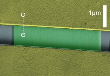
The measured suspended sample was manufactured using standard PMMA-based e-beam lithographic techniques on a graphene piece exfoliated onto Si/SiO2 chip (see Fig. 3). The dashed white line with two circles in the figure indicates the positions at which one obtains the cross sectional view depicted in Fig. 1a; the circles correspond to the spots at which the electrochemical potential profiles (along vertical direction) are drawn in Figs. 1b and 1c. The graphene sample was contacted with Au/Cr/Au leads of thickness 5/7/50 nm, after which roughly 135 nm of the sacrificial silicon dioxide was etched away using hydrofluoric acid (HF) following the methods discussed in Refs. Khodkov et al., 2012 and Khodkov et al., 2015. Raman spectroscopy was employed to verify the single layer structure of the graphene sample. Current annealing at was used to enhance the mobility of the sample. We employed voltage bias around 1 V and a current of A/m in our cleaning process. The aspect ratio of the sample as determined before the experiments was . The capacitance aF/m2 was determined using Fabry-Pérot interference fringe measurements Oksanen et al. (2014). The mobility of the sample was calculated using the charge carrier density = (obtained from Eq. (14) in the limit of large ) and in the formula , where is the measured minimum conductivity. We find cm2/Vs near the Dirac point at cm-2. For the Fermi velocity we used the value m/s; note that owing to interaction effects at small charge density, the Fermi velocity can grow up to m/s in our sample near the Dirac point Oksanen et al. (2014). The assumption of symmetric contact capacitances (within %) was verified from the inclination of the Fabry-Pérot pattern (see Ref. Oksanen et al., 2014).
Differential conductance of the sample was measured using standard low-frequency lock-in techniques (around 35 Hz); the same excitation was also employed in our differential shot noise measurements. The noise-signal from the sample was led via a circulator to a cryogenic low noise pre-amplifier having a bandwidth of 600-900 MHz Roschier and Hakonen (2004). The amplifier provided a gain of 15 dB and the signal was further amplified at room temperature by 80 dB and band pass filtered before the Schottky diode detection. Small bonding pads of size 90 m 90 m were employed in order to keep the shunting capacitance pF negligible in our microwave noise measurements Danneau et al. (2008b). For calibration purposes, a microwave switch was used to select a tunnel junction as the noise source instead of the sample. For details of the calibration procedure, see Ref. Danneau et al., 2008b. In our experiments, we employ the excess Fano factor obtained from the noise: , where we use the difference of the current noise spectrum between bias voltage mV and . The experiments were performed around 0.5 K in a Bluefors BF-LD250 dilution refrigerator.
IV Measurements and Results
Before presenting our data and their analysis, let us first summarize the free parameters that enter our theoretical model. The capacitances are fixed by the geometry and the charge dipole layer thickness , which equals to Å according to the calculation of Ref. Giovannetti et al., 2008 for graphene/gold interface; assuming corresponds to in Fig. 1, this yields F/cm2 using the vacuum permittivity. There are three parameters that are fitted to the data: , , and the thickness of the charge gradient interface. The overall magnitude of the measured conductance sets meV in our analysis. Furthermore, the noise analysis indicates that nm (see below). Hence, we are left with one -dependent fit parameter, , which describes the electrostatic behavior of the contact regime with the gate voltage.
The zero-bias conductance as a function of is displayed in Fig. 4. The Dirac point resides at = V indicating negative dopants on the sample. However, the asymmetry of the conductance and the shot noise suggest positive doping, which would correspond to V, in contrast to the above. In order to account for the ”wrong” sign of the Dirac point location, we argue that the work function of the back gate has to play a role. The work function of doped silicon depends on the sign and amount of the dopants. At large negative doping, eV for our background material with a negative dopant concentration of cm-2 Novikov (2010). Since eV according to Ref. Oshima and Nagashima, 1997, we obtain V, which leads to at V. Hence our data are consistent with doping induced by the work function of the backgate material.
As in earlier works, we characterize our results in terms of the odd part of the resistance across the Dirac point, with counted from the Dirac point, we find at carrier density cm-2, which is consistent with other experiments Huard et al. (2007, 2008); Stander et al. (2009). The conductance at large positive is substantially smaller than at equal carrier density at as expected in the presence of -interfaces. The overlaid curves in Fig. 4 represent the fits of the model for each gate voltage value using the Fermi level position as the fitting parameter, with set values for the thickness nm and for the work function difference meV; further input parameters of the model are specified in Sect. II.1. Since the fitting is done separately at each point, there is no difference between the overlaid curve and the data.
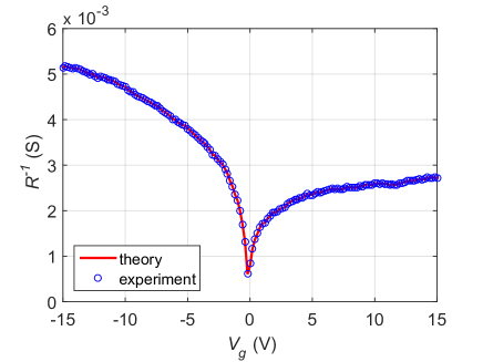
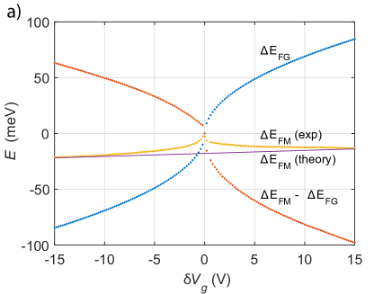
Fig. 5a depicts the Fermi level shift in the contact regions, obtained from the point-wise fitting of our model to the conductance data in Fig. 4. The Fermi level does not move much with , which is due to a large contact capacitance when compared with the other capacitances in the system (see Eq. (10)). Neglecting the region around the Dirac point, changes almost linearly with gate voltage due to the additional charge induced by to the contact region. This is expected from our model, and by fitting Eq. (10) to our data in Fig. 5a we obtain meV, F/cm2, and F/cm2, close to the geometrical estimates discussed earlier. Taking into account the uncertainties in the involved capacitances, the asymptotic agreement between the experiment and the theoretical model can be considered as good.
Additional effects are observed near the Dirac point . The doping becomes close to zero, and clearly our electrostatic model does not capture the behavior completely. One shortcoming, for example, is that we do not include the renormalization of Fermi velocity by interactions near the Dirac point, which would partly improve the agreement between Eq. (10) and the measured data. Also near the Dirac point evanescent waves become important, but they can be neglected when working at finite . Finally, another explanation could be the formation of charge puddles, which exist in suspended graphene even though their strength is suppressed compared with non-suspended samples Du et al. (2008). These phenomena are beyond our present analysis.
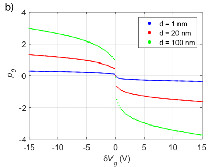
Fig. 5a displays our experimental results for and the difference . Once is known, we may evaluate the impact parameter , which is depicted in Fig. 5b. We note that the value of the impact parameter is proportional to (when is fixed, ), apart from small corrections. At large interface thickness, our data approaches the regime of validity of the analysis by Sonin Sonin (2009). According to Eq. (18), the dependence of the slope of in our barrier is given by when the interface thickness is fixed.
Last, we present our data on the Fano factor. We employed a bias voltage mV in our measurements in order to be well above the cross-over voltage between thermal and shot noise, as well as to reach clearly the regime where the incoherent summation of barrier transmissions becomes valid (see Subsection II.3). The experimental data measured at mV are presented in Fig. 6 together with the curves given by our theoretical formula in Eq. (34) for interface thicknesses , 20, and 100 nm between the doping sections dominated by the metal and the backgate. The dependence of the calculated Fano factor with the interface thickness is found to be rather weak below nm.
As with resistance, we have analyzed the odd part of the Fano factor, , which would be independent of spurious, common contributions due to scattering on both sides of the Dirac point. For example at mV, we find an asymmetric maximum at cm-1 above which decreases smoothly from down to 0.03 at charge density of cm-2. The experimentally obtained value and the slow decrease with correspond well to the theoretical behavior.
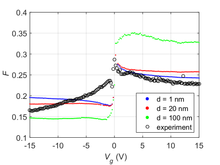
Our noise data clearly display asymmetry that is expected for Klein tunneling. Our model yields Fano factors that are in good agreement with the measured results at (the case with -interfaces) when the interface thickness is set to 1 nm. Thick interfaces on the order of 100 nm do not fit the results whereas intermediate thicknesses nm and below fit reasonably well. Consequently, we conclude that nm on the basis of our shot noise results.
At , our model predicts a clear drop in the Fano factor with decreasing and then a subsequent gradual recovery with lowering electrochemical potential. The data displays similar features but the scale appears much smaller. The calculated Fano factor at appears to be in agreement with the data on average . The data display a clear dip on the negative gate voltage side. Asymptotically, there is a clear difference in the calculated Fano factors, as in the experimental results. The agreement could be improved by adding a fitting parameter to account for a small reduction of contact transparency, but here we have set the contact transparency in order to avoid an additional fit parameter. We believe that these differences are mostly caused by non linear screening effects which are known to be different at the Dirac point and away from it Zhang and Fogler (2008); Khomyakov et al. (2010). Such charge density dependent screening is not included in our model.
V Discussion
In the experiments on graphene, it is common that the Fabry-Pérot type interferences remain weak even though the sample is more or less ballistic Oksanen et al. (2014). This is accordance with the starting point of our analysis in which the interference effects are neglected. Indeed, phase coherence is satisfied over small distances on the order of 20 nm (i.e. over the thickness of the barrier) as assumed in our calculations. However, the coherence is almost lost over the distance between the barriers and interferences become negligible. Besides, our noise experiments were performed at finite bias, above the regime where Fabry-Pérot oscillations were observed, which may strengthen the tendency towards incoherent behavior; in fact, electron-electron interaction effects in graphene have been found to be 100 larger in graphene than in regular metallic systems Voutilainen et al. (2011).
The work function difference including the chemical interaction was found to be related to the overall magnitude of the sample conductance, this did set meV. In our notation, corresponds to positive doping if is solely governed by . For gold contacts ( eV), DFT calculations predict eV Giovannetti et al. (2008); Khomyakov et al. (2009), but one has to keep in mind that these calculations yield the work function of pure gold with an error on the order of 0.2 eV. Experiments suggest that eV for pure gold Malec and Davidović (2011). Furthermore, Cr has a work function of eV and Cr/Au contacts have been shown to yield a work function of 4.3 eV for graphene under the contact Song et al. (2012), which leads to an estimate eV for Cr/Au contacts. The results of Ref. Nagashio et al., 2009 suggest eV for Au/Cr contact, although the authors discuss that the contact doping might be close to zero, which would be in agreement with our results. However, the exact comparison with Ref. Nagashio et al., 2009 is problematic because of the differences in the contact structure: we evaporate first 5 nm of Au before laying down 7 nm of Cr. As discussed below, the vacancy creation by the first evaporated metal layer is of major concern.
The actual electrical contacting is further complicated by the reactivity of metal atoms on top of graphene Zan et al. (2011); Ramasse et al. (2012). Using in situ X-ray photoelectron spectroscopy it has been demonstrated that sometimes the side-contacting picture may be misleading with real contacts Gong et al. (2014). In our analysis, for simplicity, we need to assume a uniform graphene layer under the metallic contact, although it is possible that metals like Cr promote vacancy formation and lead to creation of defects under the evaporated metal; similar defect formation has been reported due to deposition of gold atoms Shen et al. (2013), as well as in annealing studies of metallic contacts Leong et al. (2014). Furthermore, charge transfer at the interface depends on the amount of oxygen and nitrogen on top of graphene as has been found in functionalization studies by Foley et al Foley et al. (2015).
Despite of possible defect formation, gold contacts are known to preserve the graphene cone structure under the contact Sundaram et al. (2011); Ifuku et al. (2013). Quantum capacitance measurements of graphene under the contact were performed in Ref. Ifuku et al., 2013 to characterize the cone structures. The accuracy of these quantum capacitance determinations compared with theory is within a factor of two. These findings suggest a modification of the Fermi velocity under the contacts. An inclusion of such a modification would form a promising extension of our theory, but this was left for future.
The parameter together with gate capacitance (yielding ) determines fully the product which varies strongly with the gate voltage. Hence, our measurement imposes a constraint on the product as a function of . When the thickness of the interface is fixed, the slope of the interface approaches quickly zero as . Altogether, the range of variation of is rather limited, which indicates weak doping by contacting metal as well as by the gate ( is small for suspended devices).
The same analysis as presented here can be performed using a constant slope rather than a fixed . We did such an analysis and, somewhat surprisingly, the numerical simulations yielded similar predictions for the conductivity and Fano factor, in particular for and . This increases the confidence in the analysis of our results, demonstrating that the extraction of relevant parameters does not depend strongly on model-specific assumptions about the trapezoidal barrier in the regime of our data (i.e. at small interface thickness ).
Screening influences the speed at which charge density varies across borders between differently doped regions. Due to its peculiar inherent properties, screening in graphene may be strongly non-linear. According to theory Khomyakov et al. (2010), the screening influences mostly the asymptotic behavior of the barrier, whether it is or , but not much the length scale of the rapid initial relaxation. Since we use trapezoidal shape and neglect the relaxation behavior in the barrier altogether, we have chosen to work with fixed thickness, which is proportional to the average inverse slope of the charge relaxation at the -interface. One should keep in mind that our analysis is not reliable close to the Dirac point since there the slope itself weakly affects the conductance. Therefore, our fitting is mostly sensitive to the interfacial thickness far away from the Dirac point where the screening length becomes short.
According to Ref. Khomyakov et al., 2010, the approximate thickness of the -interface could be in the range of 5 nm (see also Ref. Barraza-Lopez et al., 2010), which is consistent with our results nm. Full numerical simulations on the -interface structure in a double-gated graphene structure have been performed in Ref. Liu, 2013. Within the trapezoidal approximation, the calculated slope of the potential profile in Ref. Liu, 2013 yields an interface thickness of 30-40 nm. In our case, the leads may act as gates and, consequently, the -interfaces near the contacts remain sharp, in agreement with theoretical estimates. Our interfacial width of nm, on the other hand, is much smaller than found using scanning photocurrent microscopy on non-suspended samples fabricated on silicon dioxide Lee et al. (2008); Mueller et al. (2009).
Our primary fit parameter takes into account the standard electrostatics in the contact region. Our analysis indicates a clear success of electrostatic analysis, and the results verify the role of large contact capacitance arising due to charge transfer between the contact metal and graphene. This leads to pinning of Fermi level at the contact, which is consistent with findings in Refs. Lee et al., 2008 and Mueller et al., 2009. Near the Dirac point, we find modifications from the standard electrostatic doping picture, which are presumably related with the neglect of proper screening treatment and nonuniformities in the charge distribution near the Dirac point.
Finally, our analysis is based on a rather idealized theoretical model. Additional effects can be included in to our theoretical model, for example the broadening of the density of states in the graphene due to inhomogeneities and due to coupling to metal. Clearly, the inclusion of these effects would broaden the conductance and the Fano factor characteristics, resulting in a better fit with our experimental data. The disadvantage of this phenomenological approach is that supplementary knowledge on additional parameters would be needed. We did check, however, what happens if a finite contact resistance is included using Eq. (35). From the simulations, we find that a significant discrepancy in the overall value of the Fano factor starts to appear for : the Fano factor increases quickly over the entire gate voltage range and the fitting becomes difficult, no matter how large doping is used. This constrains the value of to , but the improvements in the fitting achieved within this range are negligibly small.
In conclusion, we have developed a practical transport model for analyzing transport in ballistic, suspended graphene samples. Our analysis shows how the doping in graphene depends on the difference between the work function of the metal and graphene as well as on the applied gate voltage measured from the Dirac point which is given by the work function difference between the backgate material and graphene. By combining conductance and shot noise experiments performed on a high-quality suspended graphene sample, we have determined all the relevant parameters which are involved in the electrostatics of the contact and in the Klein tunneling of graphene. When comparing with DFT calculations Giovannetti et al. (2008), we find a semiquantitative agreement for the graphene-modified metal work functions as well as for the distance between the charge separation layers which govern the contact capacitance between the metal and graphene. The small charge layer separation ( Å) leads to a large contact capacitance which is responsible for a rather weak tunability of the Fermi level position under the contact.
Acknowledgements
We acknowledge fruitful discussions with D. Cox, V. Falko, T. Heikkilä, M. Katsnelson, M.-H. Liu, and A. De Sanctis. Our work was supported by the Academy of Finland (contract 250280, LTQ CoE) and by the Graphene Flagship project. This research project made use of the Aalto University Cryohall infrastructure. S.R. and M.F.C acknowledge financial support from EPSRC (Grant no. EP/J000396/1, EP/K017160/1, EP/K010050/1, EPG036101/1, EP/M001024/1, EPM002438/1) and from Royal Society international Exchanges Scheme 2012/R3 and 2013/R2.
Appendix A The Fermi electric flux
The Fermi electric flux
| (36) |
is related to the concept of quantum capacitance per unit area of graphene,
| (37) |
where is the number of excess (negatively charged) carriers per unit area, is the density of states of graphene, and is the energy of the Fermi level measured from the Dirac point,
| (38) |
Another useful formula is . With these notations one immediately obtains
| (39) |
resembling the formula for the energy of a capacitor charged by a fixed voltage . Therefore the Fermi electric flux is the electric flux through the plates of a capacitor of unit area and unit distance between the plates, with capacitance equal to the quantum capacitance and charged to an electrostatic energy .
The Fermi electric flux is a useful constant also for studying the inductive properties of graphene. The duality between the electric and magnetic properties is manifested in this case through the simple relation , where is the flux quantum. Then, the graphene kinetic inductance can be defined by regarding the Fermi energy as a magnetic energy associated with the magnetic flux , yielding
| (40) |
in agreement with the known result for the kinetic inductance of graphene Yoon et al. (2014).
Another connection can be made with the fine structure constant, , which has an essential role in determining the optical properties of graphene Nair et al. (2008). We obtain
| (41) |
Similarly, one can introduce a graphene fine structure constant , obtaining .
Appendix B Conductance for the whole barrier
Equation (32) is well known in mesoscopic physics and can be found in some textbooks, e.g. by S. Datta Datta (1995) and by Yu. Nazarov & Ya. Blanter Nazarov and Blanter (2009). It is derived by summing over all the Fabry-Pérot reflection and transmission processes and neglecting the interference term in the final result Datta (1995). Here we give an alternative, simpler proof, starting from the beginning with the assumption that the currents simply add up without any interference term.
We consider the generic problem of incoherent tunneling through two interfaces, interface 1 separating the left region from a middle region and interface 2 separating the middle region from the right region, see Fig. 7. Typically in this type of problems, the middle region is associated with a barrier, so we will denote it as such. The barrier has transmission coefficients on the left side and on the right side; the corresponding reflection coefficients are denoted by and .
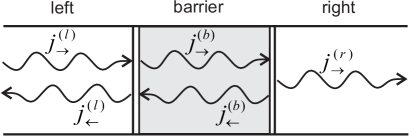
We assume that a wave producing a current propagates from the left region towards the barrier. Part of this wave will get reflected back to the left into , and part of it gets transmitted in the region under the barrier , with the current . At the right side of the barrier, the incoming current gets transmitted to the region on the right of the barrier as and part of it is reflected back under the barrier as . The wave travels backwards (to the left) towards the left side of the barrier, where it is partly reflected and partly transmitted, contributing to and respectively. By using the fact that in the absence of interference the currents will just sum up, we get
| (42) | |||||
| (43) | |||||
| (44) | |||||
| (45) |
Adding the first pair of equations Eqs. (42-43) yields the conservation law for the current at the interface, , while adding the second pair Eqs. (44-45) gives the conservation law at the interface, . From these two equations we get , which is a conservation law across the entire barrier. Finally, by combining the Eqs. (42-44) above we get
| (46) |
from which we can read directly the overall transmission coefficient across the barrier, . For this yields
| (47) |
which was given in Eq. (32) of the main text. Similarly, from Eqs. (43-45) we obtain
| (48) |
from which we get the overall reflection coefficient across the barrier. .
Appendix C Finite bias
The model presented in the paper does not include the small voltage bias used in the experiment to create a nonzero electric current between the left and the right contacts. A small finite bias voltage can be easily included, as detailed below. We assume that this bias is equally distributed, between the left metal and the graphene and between the right metal and the graphene sheet. We also assume that the currents are small enough so that the equilibrium structure of the energy levels in graphene is not considerably changed. The bias only provides a slightly higher Fermi level in the metal from which electrons are injected at the left side and holes are injected at the right side. Due to electron-hole symmetry, the total current and the total noise can be calculated by adding the contributions corresponding to electron and hole transport Sonin (2008).
The electron injected from the left into the graphene sheet will have a Fermi energy shift in the metal contact region , and a Fermi energy shift in the suspended region. Similarly, for the hole injected from the right side, we will have the shifts and . The current at a bias voltage can be calculated in this model by taking into account that this voltage will be distributed onto both junctions, . The measured conductance for a bias voltage is defined as , yielding
| (49) |
Similarly, the differential noise for a bias voltage is
| (50) |
and the Fano factor becomes
| (51) |
In these equations, and are the same as and introduced in Sec. II, but are now calculated for electrons with energies , shifted from the equilibrium values calculated in Eqs. (10) and (14), and correspondingly shifted momenta (see Eqs. (22) and ( 29)), and . To summarize,
| (52) | |||||
| (53) |
where is defined according to Eq. (32), but at energies , and at shifted momenta , .
Note that due to the assumptions above, the impact parameter and the slope will not change, since these are calculated from the equilibrium values , and . Using this modified model we can account for the effect of a small bias voltage. The simulation show that, as expected, that this produces a slight broadening of the ideal (zero-bias) conductance and Fano factor, and does not have a significant effect for the determination of the doping parameters.
References
- Tworzydlo et al. (2006) J. Tworzydlo, B. Trauzettel, M. Titov, A. Rycerz, and C. Beenakker, Phys. Rev. Lett. 96, 246802 (2006).
- Katsnelson et al. (2006) M. I. Katsnelson, K. S. Novoselov, and A. K. Geim, Nat. Phys. 2, 620 (2006).
- Katsnelson (2006) M. I. Katsnelson, Eur. Phys. J. B 51, 157 (2006).
- Miao et al. (2007) F. Miao, S. Wijeratne, Y. Zhang, U. C. Coskun, W. Bao, and C. N. Lau, Science 317, 1530 (2007).
- Danneau et al. (2008a) R. Danneau, F. Wu, M. Craciun, S. Russo, M. Tomi, J. Salmilehto, A. Morpurgo, and P. Hakonen, Phys. Rev. Lett. 100, 196802 (2008a).
- Du et al. (2008) X. Du, I. Skachko, A. Barker, and E. Y. Andrei, Nat. Nanotechnol. 3, 491 (2008).
- Sonin (2008) E. B. Sonin, Phys. Rev. B 77, 233408 (2008).
- Cheianov and Fal’ko (2006) V. V. Cheianov and V. I. Fal’ko, Phys. Rev. B 74, 041403(R) (2006).
- Shytov et al. (2008) A. Shytov, M. Rudner, and L. Levitov, Phys. Rev. Lett. 101, 156804 (2008).
- Cayssol et al. (2009) J. Cayssol, B. Huard, and D. Goldhaber-Gordon, Phys. Rev. B 79, 075428 (2009), arXiv:arXiv:0810.4568v2 .
- Huard et al. (2007) B. Huard, J. Sulpizio, N. Stander, K. Todd, B. Yang, and D. Goldhaber-Gordon, Phys. Rev. Lett. 98, 236803 (2007).
- Huard et al. (2008) B. Huard, N. Stander, J. Sulpizio, and D. Goldhaber-Gordon, Phys. Rev. B 78, 121402 (2008).
- Stander et al. (2009) N. Stander, B. Huard, and D. Goldhaber-Gordon, Phys. Rev. Lett. 102, 026807 (2009).
- Rickhaus et al. (2013) P. Rickhaus, R. Maurand, M.-H. Liu, M. Weiss, K. Richter, and C. Schönenberger, Nat. Commun. 4, 2342 (2013).
- Oksanen et al. (2014) M. Oksanen, A. Uppstu, A. Laitinen, D. J. Cox, M. F. Craciun, S. Russo, A. Harju, and P. Hakonen, Phys. Rev. B 89, 121414 (2014).
- Novikov (2007) D. S. Novikov, Appl. Phys. Lett. 91, 102102 (2007).
- Chen et al. (2008) J.-H. Chen, C. Jang, S. Adam, M. S. Fuhrer, E. D. Williams, and M. Ishigami, Nat. Phys. 4, 377 (2008).
- Young and Kim (2009) A. F. Young and P. Kim, Nat. Phys. 5, 222 (2009).
- Young and Kim (2011) A. F. Young and P. Kim, Annu. Rev. Condens. Matter Phys. 2, 101 (2011).
- Liu et al. (2008) G. Liu, J. Velasco, W. Bao, and C. N. Lau, Appl. Phys. Lett. 92, 203103 (2008).
- Gorbachev et al. (2008) R. V. Gorbachev, A. S. Mayorov, A. K. Savchenko, D. W. Horsell, and F. Guinea, Nano Lett. 8, 1995 (2008).
- Ferrari (2014) A. C. Ferrari, Nanoscale 7, 4598 (2014).
- Tielrooij et al. (2015) K. J. Tielrooij, L. Piatkowski, M. Massicotte, A. Woessner, Q. Ma, Y. Lee, K. S. Myhro, C. N. Lau, P. Jarillo-Herrero, N. F. van Hulst, and F. H. L. Koppens, Nat. Nanotechnol. 10, 437 (2015).
- Giovannetti et al. (2008) G. Giovannetti, P. Khomyakov, G. Brocks, V. Karpan, J. van den Brink, and P. Kelly, Phys. Rev. Lett. 101, 026803 (2008).
- Sonin (2009) E. Sonin, Phys. Rev. B 79, 195438 (2009).
- Xia et al. (2011) F. Xia, V. Perebeinos, Y.-m. Lin, Y. Wu, and P. Avouris, Nat. Nanotechnol. 6, 179 (2011).
- Fang et al. (2007) T. Fang, A. Konar, H. Xing, and D. Jena, Appl. Phys. Lett. 91, 092109 (2007).
- Fogler et al. (2008) M. M. Fogler, D. S. Novikov, L. I. Glazman, and B. I. Shklovskii, Phys. Rev. B 77, 075420 (2008).
- Das Sarma et al. (2012) S. Das Sarma, S. Adam, E. H. Hwang, and E. Rossi, Rev. Mod. Phys. 83, 407 (2012).
- Khodkov et al. (2012) T. Khodkov, F. Withers, D. Christopher Hudson, M. Felicia Craciun, and S. Russo, Appl. Phys. Lett. 100, 013114 (2012).
- Khodkov et al. (2015) T. Khodkov, I. Khrapach, M. F. Craciun, and S. Russo, Nano Lett. 15, 4429 (2015).
- Roschier and Hakonen (2004) L. Roschier and P. Hakonen, Cryogenics (Guildf). 44, 783 (2004).
- Danneau et al. (2008b) R. Danneau, F. Wu, M. F. Craciun, S. Russo, M. Y. Tomi, J. Salmilehto, A. F. Morpurgo, and P. J. Hakonen, J. Low Temp. Phys. 153, 374 (2008b).
- Novikov (2010) A. Novikov, Solid. State. Electron. 54, 8 (2010).
- Oshima and Nagashima (1997) C. Oshima and A. Nagashima, J. Phys. Condens. Matter 9, 1 (1997).
- Zhang and Fogler (2008) L. M. Zhang and M. M. Fogler, Phys. Rev. Lett. 100, 116804 (2008).
- Khomyakov et al. (2010) P. A. Khomyakov, A. A. Starikov, G. Brocks, and P. J. Kelly, Phys. Rev. B 82, 115437 (2010).
- Voutilainen et al. (2011) J. Voutilainen, A. Fay, P. Häkkinen, J. K. Viljas, T. T. Heikkilä, and P. J. Hakonen, Phys. Rev. B 84, 045419 (2011).
- Khomyakov et al. (2009) P. A. Khomyakov, G. Giovannetti, P. C. Rusu, G. Brocks, J. van den Brink, and P. J. Kelly, Phys. Rev. B 79, 195425 (2009).
- Malec and Davidović (2011) C. E. Malec and D. Davidović, Phys. Rev. B 84, 033407 (2011).
- Song et al. (2012) S. M. Song, J. K. Park, O. J. Sul, and B. J. Cho, Nano Lett. 12, 3887 (2012).
- Nagashio et al. (2009) K. Nagashio, T. Nishimura, K. Kita, and A. Toriumi, 2009 IEEE Int. Electron Devices Meet. 23, 2.1 (2009).
- Zan et al. (2011) R. Zan, U. Bangert, Q. Ramasse, and K. S. Novoselov, Nano Lett. 11, 1087 (2011).
- Ramasse et al. (2012) Q. M. Ramasse, R. Zan, U. Bangert, D. W. Boukhvalov, Y.-W. Son, and K. S. Novoselov, ACS Nano 6, 4063 (2012).
- Gong et al. (2014) C. Gong, S. Mcdonnell, X. Qin, A. Azcatl, H. Dong, Y. J. Chabal, K. Cho, and R. M. Wallace, , 642 (2014).
- Shen et al. (2013) X. Shen, H. Wang, and T. Yu, Nanoscale 5, 3352 (2013).
- Leong et al. (2014) W. S. Leong, Chang Tai Nai, and J. T. L. Thong, Nano Lett. 14, 3480 (2014).
- Foley et al. (2015) B. M. Foley, S. C. Hernández, J. C. Duda, J. T. Robinson, S. G. Walton, and P. E. Hopkins, Nano Lett. 15, 4876 (2015).
- Sundaram et al. (2011) R. S. Sundaram, M. Steiner, H.-Y. Chiu, M. Engel, A. A. Bol, R. Krupke, M. Burghard, K. Kern, and P. Avouris, Nano Lett. 11, 3833 (2011).
- Ifuku et al. (2013) R. Ifuku, K. Nagashio, T. Nishimura, and A. Toriumi, Appl. Phys. Lett. 103, 033514 (2013).
- Barraza-Lopez et al. (2010) S. Barraza-Lopez, M. Vanević, M. Kindermann, and M. Y. Chou, Phys. Rev. Lett. 104, 076807 (2010).
- Liu (2013) M.-H. Liu, J. Comput. Electron. 12, 188 (2013).
- Lee et al. (2008) E. J. H. Lee, K. Balasubramanian, R. T. Weitz, M. Burghard, and K. Kern, Nat. Nanotechnol. 3, 486 (2008).
- Mueller et al. (2009) T. Mueller, F. Xia, M. Freitag, J. Tsang, and P. Avouris, Phys. Rev. B 79, 245430 (2009).
- Yoon et al. (2014) H. Yoon, C. Forsythe, L. Wang, N. Tombros, K. Watanabe, T. Taniguchi, J. Hone, P. Kim, and D. Ham, Nat. Nanotechnol. 9, 594 (2014).
- Nair et al. (2008) R. R. Nair, P. Blake, A. N. Grigorenko, K. S. Novoselov, T. J. Booth, T. Stauber, N. M. R. Peres, and A. K. Geim, Science 320, 1308 (2008).
- Datta (1995) S. Datta, Electronic transport in mesoscopic systems (Cambridge University Press, 1995).
- Nazarov and Blanter (2009) Y. V. Nazarov and Y. M. Blanter, Quantum Transp. Introd. to Nanosci. (Cambridge University Press, 2009).