Snake Trajectories in Ultraclean Graphene p-n Junctions
Snake states are trajectories of charge carriers curving back and forth along an interface. There are two types of snake states, formed by either inverting the magnetic field direction or the charge carrier type at an interface. Whereas the former has been demonstrated in GaAs-AlGaAs heterostructures, the latter has become conceivable only with the advance of ballistic graphene where a gapless p-n interface governed by Klein tunneling can be formed. Such snake states were hidden in previous experiments due to limited sample quality. Here we report on magneto-conductance oscillations due to snake states in a ballistic suspended graphene p-n-junction which occur already at a very small magnetic field of mT. The visibility of is enabled by Klein collimation. Our finding is firmly supported by quantum transport simulations. We demonstrate the high tunability of the device and operate it in different magnetic field regimes.

A magnetic field fundamentally modifies the transport properties of an electronic conductor by acting on its charge carriers via the Lorenz force. The most prominent magnetotransport effect is the quantum Hall effect in a two-dimensional electron gas (2DEG). A strong perpendicular magnetic field forces the charge carriers into one-dimensional conduction channels that flow along the edges of a sample. At moderate magnetic fields however electron trajectories can be understood in a quasiclassical picture where the Lorenz force bends charge carriers into cyclotron orbits. At the boundary of a conductor charge carriers are not localized and can propagate via so-called skipping orbits. Magnetic focusing experimentsvanHouten1989 ; Taychatanapat2013 represent a direct proof of the skipping orbit picture. In such experiments an increase of conductance is observed if the distance between two contacts is an integer multiple of the diameter of a cyclotron orbit. One condition for the observation of such trajectories is ballistic transport over the relevant device dimensions. This has limited the observation of skipping orbits to the cleanest available semiconductor samples.
Since 2004 graphene as a new two-dimensional conductor has moved into the focus of condensed matter research and its behaviour in magnetic field has been intensely investigated. The quality of graphene devices has improved over the recent years and ballistic transport over distances of several microns have been demonstrated recently Rickhaus2013 ; Grushina2013 . Since graphene is a gap-less semiconductor, it offers the possibility of creating internal interfaces with opposite charge carrier polarity. These so-called p-n interfacesHuard2007 ; Ozyilmaz2007 ; Gorbachev2008 are formed by local electrostatic gating.
If electrons that propagate via skipping orbits encounter such a p-n interface, they will turn into snake states. These states consist of alternating half circles with opposite chirality and they transport current along the interface. Similar snake states have first been realized in GaAs/AlGaAs 2DEGs by defining regions of alternating magnetic field direction Ye1995 . These states share the condition of commensurability (similar to the above described magnetic focusing experiments) with p-n snake states but they do not propagate along a single and tunable interface. Snake states in graphene p-n junctions were claimed to have been observed in disordered substrate supported samplesWilliams2011 but the experiment lacked of direct evidence for snaking trajectories.
In this article we investigate ballistic transport across a graphene p-n junction in different magnetic field regimes and identify magneto-conductance oscillations as a direct signature of snake states. These findings are supported by detailed tight-binding simulations that allow us to visualize the alternating cyclotron orbits of the snake states.
I results
I.1 Evolution of electron trajectories in graphene p-n junction
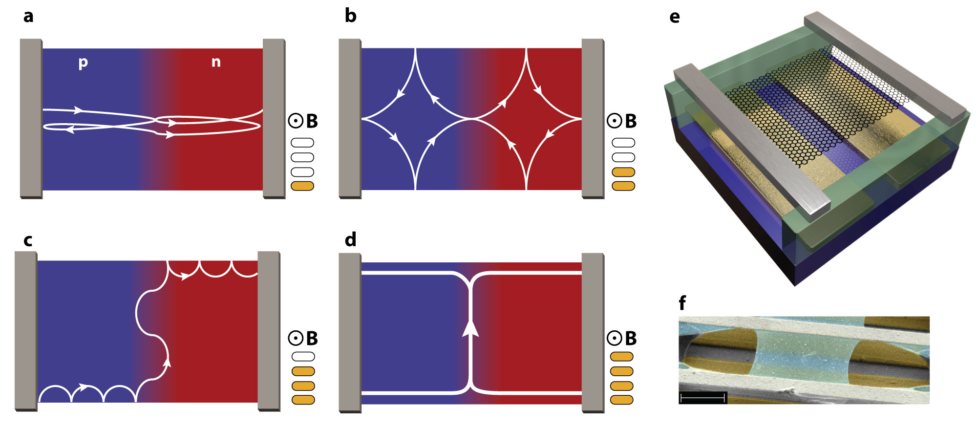
In figure 1a-d we illustrate schematically how trajectories under increasing perpendicular magnetic field evolve in such a device. Figure 1a describes the low-field situation where transport is still dominated by Fabry-Pérot oscillations with slightly bent trajectories Young2009 . As the field is increased resonant scar states (fig. 1b) may occur, as observed in semiconductor quantum dots Bird1999 . At higher fields (fig. 1c) snake states at the p-n interface govern the electronic properties. Finally (fig. 1d) the system enters the quantum Hall regime Novoselov2005 ; Zhang2005 where transport is dominated by edge states and Landau level mixing at the p-n interface can occur Williams2007 ; Abanin2007 . Even though this article is focusing on snake states, we will discuss the phenomenology of the mentioned magnetic field regimes. By doing so we present an integral picture of graphene p-n physics in magnetic field.
I.2 Device architecture
Figure 1e shows the design of the measured device and figure 1f a scanning electron microscope picture of a similar sample. In a suspended m graphene sheet a p-n junction is formed by applying different voltages on the left () and right () bottom-gates, resulting in different charge carrier concentrations and . The fabrication follows partly ref. Tombros2011 which we combined with a wet transfer process allowing us to align the graphene with the bottom-gates. For details see ref. Maurand2014486 and Methods.

I.3 Measurements in the Fabry-Pérot and quantum Hall regime
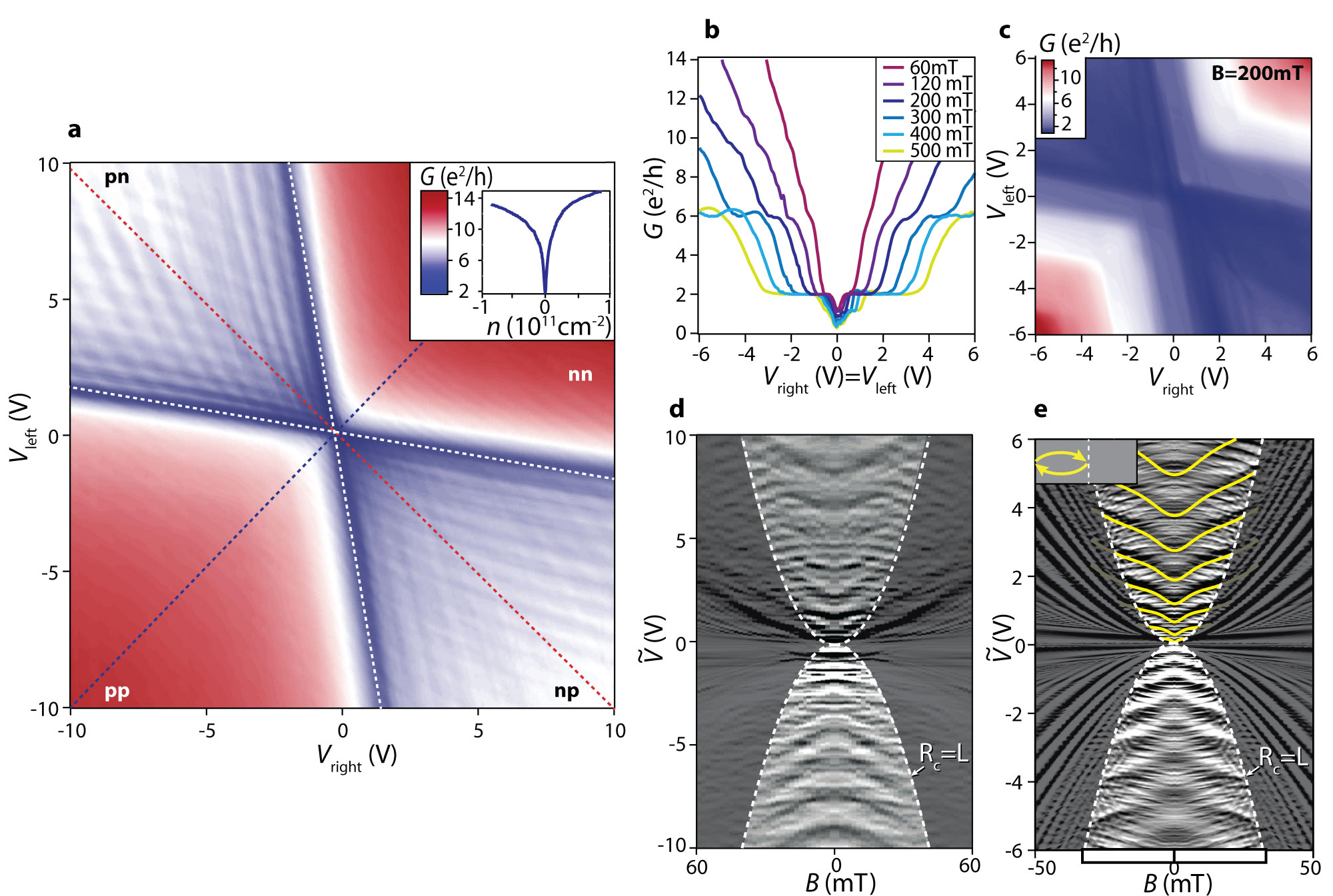
In the following we characterize the measured device in the zero, low- and high-field regimes. Figure 2a shows a two-dimensional color map of the electrical conductance . As soon as a p-n interface is formed, is lowered drastically. Regular Fabry-Pérot resonances in the left/right cavity are visible as oscillations perpendicular to the zero density line in the left/right cavity (horizontal/vertical white dashed line in fig. 2a), indicating ballistic transport Rickhaus2013 ; Grushina2013 . The inset in figure 2a is a slice along the pp-nn diagonal (blue dashed). We estimate the mobility to be cm2V-1s-1 at carrier density cm-2, which we calculated by a simple parallel plate capacitor model. The mobility is mainly limited by scattering at the contacts Cayssol2009 ; Rickhaus2013 .
In figure 2b we show cuts along the pp-nn diagonal at different magnetic fields and obtain quantum Hall plateaus at , where is the filling factor Novoselov2005 ; Zhang2005 and is the conductance quantum. Even at fields as low as mT, the plateau is visible. The colorscale map in figure 2c taken at mT shows that plateaus develop in the unipolar region with conductance values given by the lowest number of edge modes in the left or right cavity, i.e. . This observation compares well to experiments of ref. Williams2007 , even though we apply only T instead of T. In the bipolar region the conductance stays well below due to the smoothness of the p-n interface.
In a further step we study the dispersion of the Fabry-Pérot interference pattern in low magnetic field Young2009 . Figure 2d shows the numerical derivative as a function of and , where represents the magnitude of gate voltage in the situation of antisymmetric charge density (red dashed line in fig. 2a i.e. the np-pn diagonal). In this configuration the device consists of two Fabry-Pérot cavities of equal length . The darkened region where the cyclotron radius will be discussed later. In figure 2e a tight-binding transport calculation is shown which reproduces the measured interference pattern very well (for details see ref. Liu2014 and Methods). We highlight the quality of the measured graphene and the ability of the simulation to capture the complex oscillation pattern of this micron-sized system in magnetic field. The dispersion of the Fabry-Pérot oscillations can be described by bent electron trajectories such as the one sketched in the inset of figure 2e Young2009 ; Rickhaus2013 . The condition for constructive interference is met if the accumulated phase along such a trajectory is a multiple of (see “Methods”). The yellow lines in figure 2e are numerical solutions based on such a condition.

I.4 Measurement of snake states
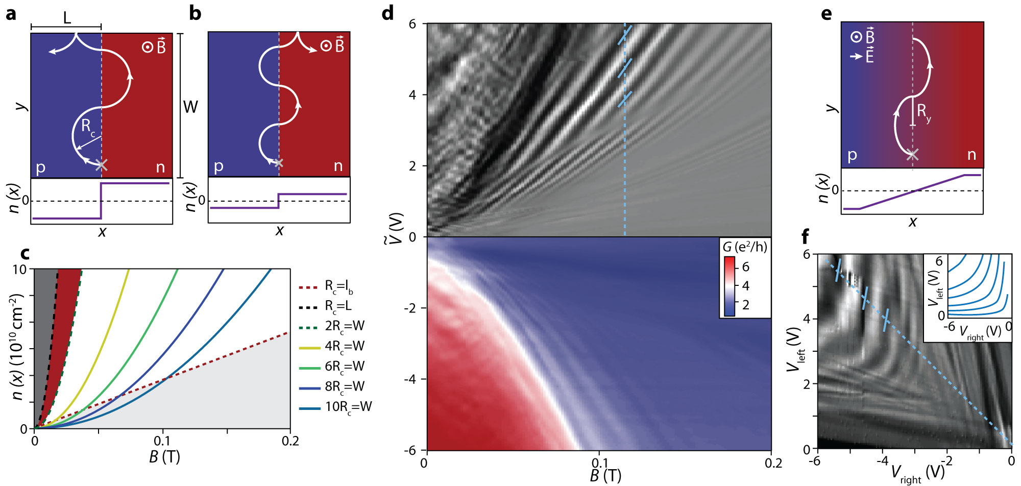
We now discuss the regime where snake states emerge. In figure 3a a snake state at a sharp p-n junction is sketched. Consider a charge carrier trajectory starting at the gray cross with momentum in direction. Due to the magnetic field the trajectory is bent towards the p-n interface within the cyclotron diameter . If the trajectory hits the p-n interface, the hole will be transmitted to the n side with high probability due to Klein tunneling Cheianov2006 . At the upper edge of the sample, the snake trajectory scatters at the left side, resulting in a current towards the left contact. At lower , is reduced. As sketched in figure 3b, the snake trajectory scatters to the right at the upper edge, resulting in a net current towards the right contact. With this mechanism one expects conductance oscillations that depend on and , and constant conductance along curves where is constant. In figure 3c we display calculated functions for constant . Snake states occur once the cyclotron diameter is smaller than the sample width (green dashed curve) and can be described by quasiclassical trajectories as long as is larger than the magnetic length (red dashed line). In the regime additional parabolic lines show the condition for which the number of oscillations in the snake pattern is fixed and commensurate with , i.e. with .
In figure 3d we show the measured conductance (bottom) and its numerical derivative (top). The measurement exhibits strong oscillations that follow parabola-like curves. We notice that the oscillations occur on a background of strongly decreasing conductance from to . The steep decrease indicates that the transport becomes dominated by the low density region close to the p-n interface and this happens when .
In a real p-n interface the density does not sharply jump from the p to the n side but evolves smoothly. An electron trajectory in such a smooth p-n interface is sketched in figure 3e. Here the density gradient leads to an electric field and its interplay with the perpendicular magnetic field results in the so-called ExB drift (here along y), leading to elongated cyclotron orbits. The condition can be studied in the measurement of figure 3f where we show at mT. The measured interference pattern follows curves of constant at the p-n interface (obtained from electrostatic simulations) as shown in the inset.

I.5 Tight-binding theory of snake states
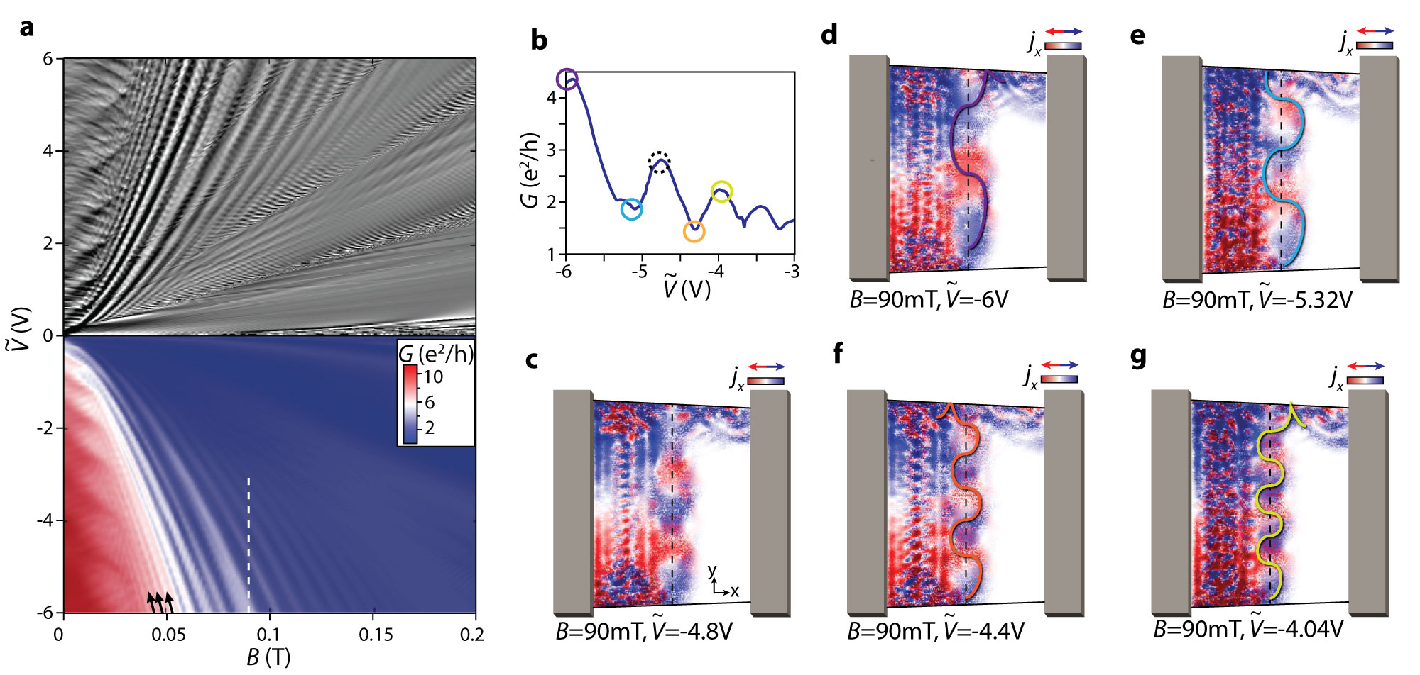
So far we have seen that the oscillation pattern occurs in the regime where snake states are expected (i.e. ) and that the oscillations are related to transport along the p-n interface. We now present a quantitative comparison between experiment and theory. Figure 4a shows a quantum transport simulation of and based on a scalable tight-binding model Liu2014 that fully takes into account the device geometry. The simulation compares very well to the measurement shown in figure 3d. The parabola-like patterns are reproduced and a similarly steep decrease of conductance is obtained. In figure 4b a slice following the white dashed line in figure 4a is shown. The visibility of the oscillations reaches in theory and experiment and is enabled by the strong Klein collimation at the smooth p-n-interface.
Next we apply the Keldysh-Green’s function method to extract local current density profiles (see Methods) at high and low conductance along this line. In figure 4c we show the -component of the current density , taken at V (dashed circle in fig. 4b). The current is injected from the left contact using a small DC offset. In the left cavity a complex resonance pattern appears, given by so-called ”bubbling” trajectories Carmier2011 which are reflected before reaching the p-n interface and do not contribute to current between the contacts. The pattern relevant for transport is located at the p-n interface (dashed line). We observe that changes sign along the p-n-interface and that the blue and red regions penetrate the dashed line, indicating that transport is dominated by Klein-collimated snake trajectories. As a guide to the eye we added a curve in figures 4d-g that follows the snake state. This is done for different values for which is maximal/minimal at a fixed magnetic field of mT (colored circles in fig. 4b). In figure 4d for example, the current density profile corresponds to a conductance maximum where the current points to the right at the upper edge of the p-n interface. One period is added by changing from one maximum to the next. More current density profiles evolving with at fixed mT are shown in Supplementary Movie 1. By tracing along one of the parabolic-like patterns, the current density profile of the snake state stays constant (an example is given in Supplementary Movie 2).
The conductance oscillates as a function of the ratio , the exact snake period corresponding to is, however, difficult to determine using quasiclassical trajectories, since current is injected from many points under various angles resulting in a complex cusp structure similar to what was predicted in refs Davies2012 ; Patel2012 ; Milovanovic2013 ; Milovanovic2014 . The excellent agreement between measurement and calculated conductance for which we could determine local current density profiles clearly indicates that the oscillations result from snake state trajectories.
There are additional parabola-like structures at lower magnetic field indicated by arrows in figure 4a, these structures are however less pronounced in the experimental data. Those resonances occur in a regime where scar states (fig. 1b) would be expected. The parabola-like behaviour indicates that the states are commensurate with a cavity dimension. In the model, the resonances disappear for non-reflective contacts as expected for scar states.
II Discussion
We investigated magneto-conductance of a ballistic graphene p-n-junction in the different magnetic field regimes. We have observed resonance patterns occurring in the intermediate quasi-classical regime in experiment and theory which result from the formation of snake states at the p-n interface. Among many other possibilities these states can be used to guide electrons on arbitrary paths with a high efficiency even at very low magnetic fields. This could be used to guide electrons away from sample edges to suppress uncontrolled momentum or spin-scattering. The directional scattering at the sample boundaries could be used to implement multi-terminal switches Chen2012a ; Milovanovic2013 . Furthermore, the similarity between Andreev reflection and Klein tunneling is stressed in theory Beenakker2008 leading to a correspondence of snake states and Andreev edge states which are of theoretical Hoppe2000 and experimental Rickhaus2012 interest. Our work points out that snake states are highly tunable, occur at low fields and that ballistic graphene p-n-junctions in magnetic field reveal novel and intriguing phenomena.
III Methods
Experimental methods. High quality graphene is obtained by in situ current annealing Moser2007 . All measurements were performed in a variable temperature Helium cryostat with a base temperature of K. We measured differential conductance by standard lock-in technique applying an AC voltage of mV at Hz.
For the quantum Hall data of figure 2b-c we subtracted a contact resistance of k.
We extracted the cavity length used in figure 2d-e from the spacing between resonant Fabry-Pérot peaks in the bipolar situation and obtained m.
Simulation methods. Real-space Green’s function method in the tight-binding framework using a scaled graphene Hamiltonian Liu2014 is applied to simulate ballistic quantum transport in the present device, taking into account the realistic on-site energy profile obtained by three-dimensional electrostatic simulation for the self-partial capacitances of the bottom gates. All the presented conductance simulations are obtained by calculating the transmission function at zero temperature, combined with the contact resistance . Local current densities are imaged by applying the Keldysh-Green’s function method in the linear response regime Cresti2008a based on the same model Hamiltonian used for conductance simulation. At each lattice site , the bond charge current density is computed, where the summation runs over all the sites nearest to , is the unit vector pointing from to , and is the quantum statistical average of the bond charge current operator Nikolic2006 . After computing for each site, the position-dependent current density profile is imaged. In fig. 4c-g the -component is shown.
The low-field Fabry-Pérot interference contours sketched in Fig. 2e are numerically obtained from solving the resonance condition , arising from the path difference between the directly transmitted and twice reflected trajectories within the p cavity as sketched in the inset of Fig. 2e, which is found to be the major interference contribution. For such a simplified model the phase difference is given by , where is the kinetic WKB-phase, is the Aharanov-Bohm phase due to the flux enclosed by the bent orbit segments, is the Berry phase, and is a constant phase due to reflections off the two p-n junction interfaces of the p cavity (smooth at middle and sharper at the contact side). Here is the numerical average of within the p cavity. The cavity size is numerically determined and is about half of the flake length . The loop area is given by with and . The form of the Berry phase follows from the consideration of Shytov2008 with the critical field estimated by , where the critical transmission value is a parameter close to one and does not significantly influence the shape of the contours; is chosen. The contours sketched in Fig. 2e correspond to .
Acknowledgments M.-H.L. and K.R. acknowledge financial support by the Deutsche Forschungsgemeinschaft (SFB 689 and SPP 1666). This work was further funded by the Swiss National Science Foundation, the Swiss Nanoscience Institute, the Swiss NCCR QSIT, the Graphene Flagship, the ESF programme Eurographene, the EU FP7 project SE2ND, the ERC Advanced Investigator Grant QUEST, and the EU flagship project graphene.
The authors thank Andreas Baumgartner, Laszlo Oroszlany and Szabolcs Csonka for fruitful discussions.
Author contributions P.R., P.M. and E.T. fabricated the devices. Measurements were performed by P.R., P.M., R.M. and M.W. M.-H.L. performed simulations. C.S. and K.R. guided the work. All authors worked on the manuscript.
References
- [1] van Houten H, Beenakker, Williamson, Broekaart, van Loosdrecht PH, van Wees BJ, Mooij, Foxon, and Harris. Coherent electron focusing with quantum point contacts in a two-dimensional electron gas. Phys Rev B Condens Matter, 39(12):8556–8575, 1989.
- [2] Thiti Taychatanapat, Kenji Watanabe, Takashi Taniguchi, and Pablo Jarillo-Herrero. Electrically tunable transverse magnetic focusing in graphene. Nat Phys, 9(4):225–229, April 2013.
- [3] P. Rickhaus, R. Maurand, M.-H. Liu, M. Weiss, K. Richter, and C. Schönenberger. Ballistic interferences in suspended graphene. Nature Comm, 4:2342, 2013.
- [4] A. L. Grushina, D.-K. Ki, and A. F. Morpurgo. A ballistic pn junction in suspended graphene with split bottom gates. Appl. Phys. Lett., 102:223102, 2013.
- [5] B. Huard, J. A. Sulpizio, N. Stander, K. Todd, B. Yang, and D. Goldhaber-Gordon. Transport measurements across a tunable potential barrier in graphene. Phys. Rev. Lett., 98:236803, 2007.
- [6] B. Ozyilmaz, P. Jarillo-Herrero, D. Efetov, D. A. Abanin, L. S. Levitov, and P. Kim. Electronic transport and quantum hall effect in bipolar graphene p-n-p junctions. Phys. Rev. Lett., 99:166804, 2007.
- [7] R. V. Gorbachev, A. S. Mayorov, A. K. Savchenko, D. W. Horsell, and F. Guinea. Conductance of p-n-p graphene structures with ”air-bridge” top gates. Nano Lett, 8:1995–1999, 2008.
- [8] P.D. Ye, D. Weiss, and R.R. Gerhardts. Electrons in a periodic magnetic field induced by a regular array of micromagnets. Phys. Rev. Lett., 74:3013, 1995.
- [9] J. R. Williams and C. M. Marcus. Snake states along graphene p-n junctions. Phys. Rev. Lett., 107:046602, 2011.
- [10] Andrea F. Young and Philip Kim. Quantum interference and klein tunnelling in graphene heterojunctions. Nat. Phys., 5:222–226, 2009.
- [11] J. Bird, R. Akis, D. Ferry, D. Vasileska, J. Cooper, Y. Aoyagi, and T. Sugano. Lead-Orientation-Dependent Wave Function Scarring in Open Quantum Dots. Phys. Rev. Lett., 82:4691–4694, 1999.
- [12] K. S. Novoselov, A. K. Geim, S. V. Morozov, D. Jiang, M. I. Katsnelson, I. V. Grigorieva, S. V. Dubonos, and A. A. Firsov. Two-dimensional gas of massless dirac fermions in graphene. Nature, 438:197–200, 2005.
- [13] Y. Zhang, Y.-W. Tan, H. L. Stormer, and P. Kim. Experimental observation of the quantum hall effect and berry’s phase in graphene. Nature, 438:201, 2005.
- [14] J. R. Williams, L. Dicarlo, and C. M. Marcus. Quantum hall effect in a gate-controlled p-n junction of graphene. Science, 317:638–641, 2007.
- [15] D. A. Abanin and L. S. Levitov. Quantized transport in graphene p-n junctions in a magnetic field. Science, 317:641, 2007.
- [16] N. Tombros, A. Veligura, J. Junesch, J.J. van den Berg, P.J. Zomer, I.J. Vera-Marun, H.T. Jonkman, and B. van Wees. Large yield production of high mobility freely suspended graphene electronic devices on a polydimethylglutarimide based organic polymer. J. Appl. Phys, 109:093702, 2011.
- [17] R. Maurand, P. Rickhaus, P. Makk, S. Hess, E. Tovari, C. Handschin, M. Weiss, and C. Schoenberger. Fabrication of ballistic suspended graphene with local-gating. Carbon, 79:486, 2014.
- [18] J. Cayssol, B. Huard, and D. Goldhaber-Gordon. Contact resistance and shot noise in graphene transistors. Phys. Rev. B., 79:075428, 2009.
- [19] M-H. Liu, P. Rickhaus, E. Tòvari, R. Maurand, F. Tkatschenko, M. Weiss, C. Schönenberger, and K. Richter. Scalable tight-binding model for graphene. arXiv:1407.5620v1, to be published in Phys. Rev. Lett., 2014.
- [20] V. Cheianov and V. Fal’ko. Selective transmission of Dirac electrons and ballistic magnetoresistance of n-p junctions in graphene. Physical Review B, 74(4):041403, 2006.
- [21] P. Carmier, C. Lewenkopf, and D. Ullmo. Semiclassical magnetotransport in graphene n-p junctions. Phys. Rev. B., 84:195428, 2011.
- [22] Nathan Davies, Aavishkar a. Patel, Alberto Cortijo, Vadim Cheianov, Francisco Guinea, and Vladimir I. Fal’ko. Skipping and snake orbits of electrons: Singularities and catastrophes. Phys. Rev. B., 85:155433, 2012.
- [23] A. A. Patel, N. Davies, V. Cheianov, and V. I. Fal’ko. Classical and quantum magneto-oscillations of current flow near a p-n junction in graphene. Phys. Rev. B., 86:081413, 2012.
- [24] S. P. Milovanovic, M. Ramezani Masir, and F. M. Peeters. Spectroscopy of snake states using a graphene Hall bar. Applied Physics Letters, 103:233502, 2013.
- [25] S. P. Milovanović, M. Ramezani Masir, and F. M. Peeters. Magnetic electron focusing and tuning of the electron current with a pn-junction. Journal of Applied Physics, 115(4):043719, January 2014.
- [26] Jiang-chai Chen, X. C. Xie, and Qing-feng Sun. Current oscillation of snake states in graphene p-n junction. Physical Review B, 86(3):035429, July 2012.
- [27] C. Beenakker, A. Akhmerov, P. Recher, and J. Tworzydlo. Correspondence between Andreev reflection and Klein tunneling in bipolar graphene. Physical Review B, 77:075409, 2008.
- [28] H. Hoppe, U. Zulicke, and G. Schon. Andreev reflection in strong magnetic fields. Phys. Rev. Lett., 84:1804, 2000.
- [29] Peter Rickhaus, Markus Weiss, Laurent Marot, and Christian Schönenberger. Quantum hall effect in graphene with superconducting electrodes. Nano Lett., 12:1942, 2012.
- [30] J. Moser, A. Barreiro, and A. Bachtold. Current-induced cleaning of graphene. Appl. Phys. Lett., 91:163513, 2007.
- [31] A. Cresti, G. Grosso, and G. Parravicini. Electronic states and magnetotransport in unipolar and bipolar graphene ribbons. Phys. Rev. B., 77:115408, 2008.
- [32] B. Nikolić, L. Zârbo, and S. Souma. Imaging mesoscopic spin Hall flow: Spatial distribution of local spin currents and spin densities in and out of multiterminal spin-orbit coupled semiconductor nanostructures. Phys. Rev. B., 73:075303, 2006.
- [33] A. Shytov, M. Rudner, and L. Levitov. Klein Backscattering and Fabry-Pérot Interference in Graphene Heterojunctions. Phys. Rev. Lett., 101:156804, 2008.