Edge states and integer quantum Hall effect in topological insulator thin films
Abstract
The integer quantum Hall effect is a topological state of quantum matter in two dimensions, and has recently been observed in three-dimensional topological insulator thin films. Here we study the Landau levels and edge states of surface Dirac fermions in topological insulators under strong magnetic field. We examine the formation of the quantum plateaux of the Hall conductance and find two different patterns, in one pattern the filling number covers all integers while only odd integers in the other. We focus on the quantum plateau closest to zero energy and demonstrate the breakdown of the quantum spin Hall effect resulting from structure inversion asymmetry. The phase diagrams of the quantum Hall states are presented as functions of magnetic field, gate voltage and chemical potential. This work establishes an intuitive picture of the edge states to understand the integer quantum Hall effect for Dirac electrons in topological insulator thin films.
Introduction
The discovery of the integer quantum Hall effect in two-dimensional
electron gas opens a window to explore topological phases in quantum
mattersKlitzing80prl ; QHE-book . In the quantum Hall effect
the longitudinal conductance vanishes while the Hall conductance
is quantized at , where is the elementary charge
and is the Planck constant. It is known that the integer
is the topological invariant of a quantum phase, it counts the number
of conducting chiral channels at the edges of the system, and is insensitive
to the geometry of the sample, impurity, and interactions of electrons
TNKK_1982prl ; Halperin82prb ; MacDonald84prb ; Hatsugai_1993prl .
Three-dimensional topological insulator is a new class of topological
material and is characterized by the formation of the Dirac fermion
gas covering its surfaces moore2010Nature ; Hasan10rmp ; QiXL2011rmp ; Shen_book .
Soon after the discovery of three-dimensional topological insulators,
the formation of the Landau level (LL) of the surface Dirac electrons
in a strong magnetic field has been observed by the scanning tunneling
microscope QuDongxia2010science ; Analytis2010NatPhys ; Hanaguri2010prb ; Chengpeng2010prl ; FuYishuang_2014nphys
and Shubnikov-de Haas oscillations in the longitudinal conductance
QuDongxia2010science ; Analytis2010NatPhys ; Brune2011prl . It
has been known since 1980’s that the Hall conductance of massless
Dirac fermions is quantized as half integers , where .
Jackiw84prd ; Schakel91prd ; Ando98jpsj ; Gusynin_2005prl ; LeeDH_2009prl ,
and is attributed to the Berry phase of the massless Dirac
fermions acquiring from a cyclotron motion around the Fermi surface
Ando98jpsj ; Mikitik1999prl ; Igor2004prl . Usually each LL carries
one conducting channel near the edge due to the geometric distortion
of the cyclotron motion of electrons in a magnetic field. The quantum
Hall conductance is determined by the number of the edge states Halperin82prb ; MacDonald84prb .
Thus the relation between the half-quantized Hall conductance and
the number of the conducting edge channel is an open issue and has
attracted a lot of studies Gusynin_2005prl ; Dmitry2006prl ; Peres2006prb ; Zhoubin2006prb ; QiXL2008prb ; QiXL2009science ; LeeDH_2009prl ; Tkachov2010prl ; Chu-11prb ; Vafek2011prb ; Zyuzin2011prb ; Sitte2012prl ; ZhangYY2012JPCM ; liGuohong2013natcomm ; Konig2014prb .
Very recently the integer quantum Hall effect has been measured in
three-dimensional topological insulator thin films by two independent
groups XuYang2014NatPhys ; Yoshimi_2014arXiv . One group measured
a series of plateaux of 1,2,3 and in
XuYang2014NatPhys , and the other measured the plateaux of
in
Yoshimi_2014arXiv . These plateaux of the Hall conductance
are attributed to the addition of the top and bottom surface electrons,
and always yield integers in units of .
In this work we present solutions of the LLs and edge states of the surface electrons, and explore the formation of the quantum Hall effect in a topological insulator thin film. The Hall conductance is calculated by means of the Kubo formula at zero temperature, which is well quantized when the chemical potential lies between two LLs. Two distinct patterns of the quantum Hall conductance are found: is an odd integer when the LLs of the top and bottom surface electrons are degenerate in a thick film, and is an integer when structure inversion symmetry is broken in the film or the top and bottom surface electrons are coupled to open an energy gap due to the finite-size effect Lu10prb ; Shan11njp . The absence of the plateau is caused by the degeneracy of two sets of LLs, and the plateau emerges when the degeneracy is lifted by the finite-size effect or structure inversion asymmetry (SIA, which can be produced by the energy difference between the two surfaces). The width of the plateau is determined by the energy difference between the two LLs closest to zero energy. The state of can be either in the quantum spin Hall phase or trivial band insulator phase, and the quantum spin Hall effect can be easily broken down by SIA.
Results
Model. Consider a thin film of three-dimensional topological
insulator. Starting from the bulk Hamiltonian for topological insulators
ZhangHJ_09nphys ; Shen_book , the low-energy effective Hamiltonian
for the surface electrons has been derived by solving the differential
equation for the bulk bands exactly Lu10prb ; Shan11njp
| (1) |
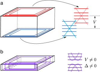
where and with the wave vector in the surface plane. The mass term is generated by the hybridization between the wave functions of the top and bottom surface electrons. Both and depend on the film thickness and approach zero simultaneously in a thick film. with the effective velocity and the reduced Planck constant. is the potential difference between the top and bottom surfaces due to SIA as shown in Fig. 1a, which can be induced in a realistic thin film by the potential difference between the substrate and vacuum surfaces, and tunable by a gate voltage. The interplay of SIA and top-bottom hybridization gives the Rashba-like splitting in the band structure (see Fig. 1b). The physics of this model has been confirmed by the angle-resolved photoemission spectroscopy experiments on topological insulator thin films ZhangY_10nphys ; Sakamoto10prb .
Two patterns of quantum Hall plateaux. For a thin film of topological insulator in the presence of a perpendicular magnetic field, the Hall conductance is usually quantized as an integer as shown in Fig. 1c, or can only be an odd integer when the LLs of the top and bottom surface electrons coincide exactly as shown in Fig. 1d. Consider a topological insulator thin film. The surface states cover the top and bottom surfaces as illustrated in Figs. 1a and 1b. The lateral side is also covered by the surface electrons, and is ignored in the present work. For a film with a relatively large thickness, the top and bottom surface states are well separated. Thus the system consists of two decoupled massless Dirac electrons. The two Dirac points can be separated by the potential difference between the top and bottom surfaces. The value of then can determine the quantized pattern of the Hall conductance such as the width of quantum plateaux and the existence of plateau. For , the LLs of the top and bottom surface electrons are degenerate, and the Hall conductance is quantized as odd integers , which can be regarded as the addition of two sets of half-quantized Hall conductance, i.e., . This is very similar to that in graphene, in which the Hall conductance is , where the factor 4 is attributed to the spin and valley degrees of freedom Novoselov2005Nature ; ZhangYB2005Nature . For , the degeneracy of the LLs is removed, and the Hall conductance becomes quantized as integers in Fig. 1c. Another factor leading to the lift of the degeneracy is the finite-size effect. When the thickness of a thin film is comparable with the spatial distribution of the wave functions of the surface states, the overlap of the wave functions will open an energy gap at the Dirac points of the two surface states Lu10prb , leading to the presence of the plateau and a possible topological phase of the quantum spin Hall effect.
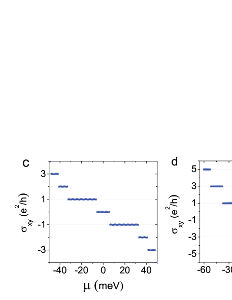
Landau levels and edge states. In Figs. 2 and 3, we present the LLs in a magnetic field normal to the thin film, the LL energies or edge states near one edge of the system, and the corresponding patterns of the quantum Hall conductance. In the absence of SIA, i.e., , four possible typical cases are shown in Fig. 2. Case (i) is for a thick film, i.e., . In the bulk, the LLs of zero energy are degenerate, and is insensitive to the field, as shown in Fig. 2a. However they split into two branches when approaching one edge: one branch goes upward (called electron-like) and the other goes downward (called hole-like), as shown in Fig. 2e. The position is the guiding center of the wave packages of surface LLs and is proportional to the wave vector , where the magnetic length . The slope of the energy dispersion near the edge is proportional to the effective velocity of the edge states , which defines the current flow of the edge states. The Hall conductance is equal to when the chemical potential is below the LLs of and when the chemical potential is above the LLs of . The plateau of is absent and other plateaux are . For a thinner film, there exist three cases, (ii), (iii) , and (iv) , all with the parameter (without loss of generality we assume negative ). In case (ii) with , the two LLs of are separated in a finite field as shown in Fig. 2b. When approaching the edge the LLs with positive energies go upward while the LLs with negative energies go downward, indicating that the edge electrons with opposite energies move in opposite directions. One of the key features of the quantum Hall conductance is the emergence of the plateau, and the width of the plateau is determined by the energy difference between the two LLs of (see Fig. 2j). In case (iii) with and , the two LLs near the Dirac point are degenerate at zero field, as shown in Fig. 2c. The degeneracy is lifted by a finite field . The energies of edge states (see Fig. 2g) and the Hall conductance (see Fig. 2k) are very similar to those in case (ii). In case (iv) with , two LLs near zero energy are separated in weak fields, and cross at a finite field as shown in Fig. 2d, indicating a quantum phase transition. In a weak field, the pattern of the Hall conductance (see Fig. 2l) is also similar to that of case (ii), while the dispersions of the edge states (see Fig. 2h) are different. The two LLs of cross near the edge, which is a key feature of the quantum spin Hall effect in a finite field Konig2007science . At magnetic fields higher than the energy crossing in Fig. 2d, the LLs near zero energy never cross near the edge, similar to those in Figs. 2 f and g, indicating the breakdown of the quantum spin Hall effect in a magnetic field. However, the plateau of still survives.
In the presence of SIA, , the relative positions of two sets of LLs from the top and bottom surfaces can be tuned by the value of . A typical pattern of the quantum Hall conductance is presented in Fig. 3. The Hall conductance covers all integers. In the case that the chemical potential crosses some accidental crossing points of two LLs, the Hall conductance can change by .
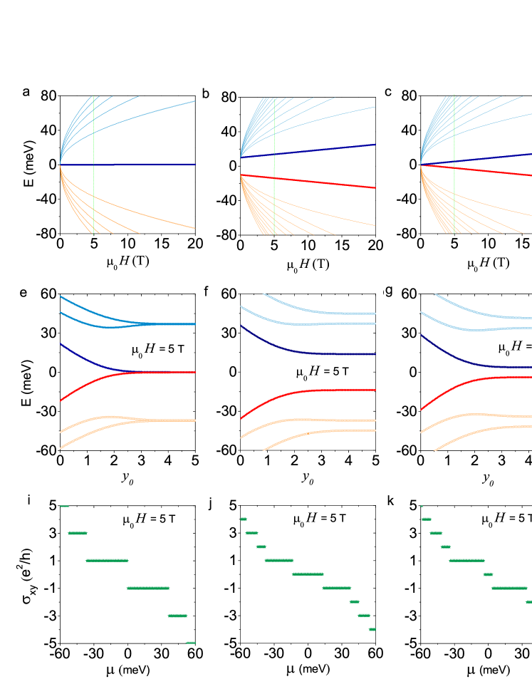
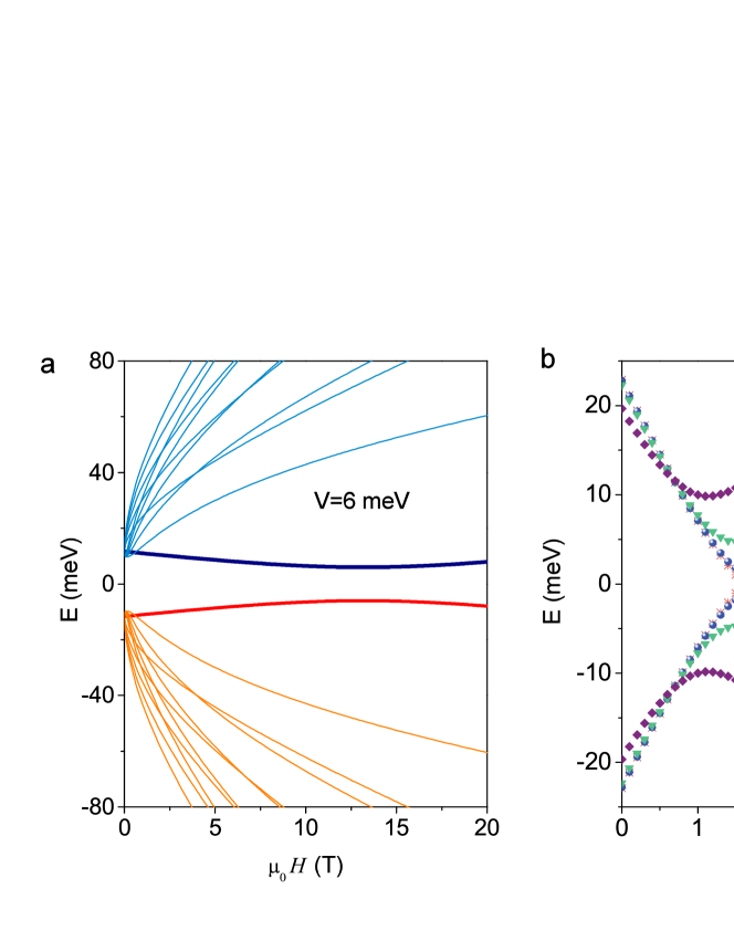
Quantum spin Hall state and its breakdown. A question arises from the appearance of the quantum spin Hall effect in case (iv) with . Usually the quantum spin Hall effect is protected by time reversal symmetry Kane2005prl ; Bernevig2006science . Applying a magnetic field breaks time reversal symmetry, but it is known from the calculation of the Hall conductance that the quantum spin Hall effect can be stabilized in a finite field when the system possesses an intrinsic and hidden symmetry which guarantees the decoupling of the two blocks with spin up and down in the Hamiltonian ZhangSB14prb . In the presence of SIA, , the situation changes. The energy crossing of the two LLs in a finite field in Fig. 2d becomes an anti-crossing for a finite in Fig. 4a, showing that there is no field-induced quantum phase transition from the quantum spin Hall insulator to the trivial band insulator in the presence of SIA and the system remains in the trivial phase at all magnetic fields. In other words, the quantum spin Hall effect breaks down as long as SIA is present. The breakdown of the quantum spin Hall phase can also be seen from the energies of the edge states in Fig. 4b, in which the energies of the LLs cross for while open a finite gap for a nonzero . The gap increases with increasing . For a small , the corresponding energy gap of the edge states is also small. Although the edge states are no longer protected topologically, it can still produce some physical phenomena such as the spin accumulation, or the intrinsic spin Hall effect near the edge when an electric current is applied. However these effects will be weakened for a large . Therefore, the quantum spin Hall effect does not survive in the presence of both a magnetic field and SIA.
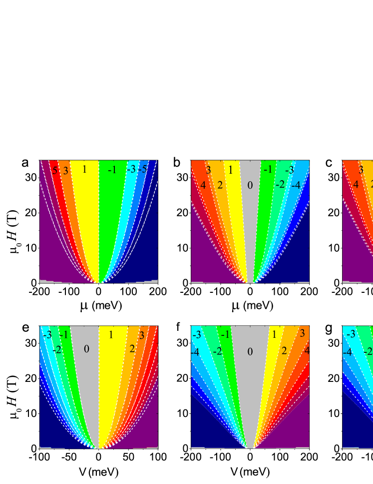
Phase diagrams. In the absence of SIA, i.e., , we plot in Figs. 5a-d the corresponding phases diagrams of the Hall conductance as a function of the chemical potential and magnetic field for the four cases. Different quantum Hall phases are denoted by the quantized Hall conductances and are separated by the boundaries (marked by the white dotted lines). The Hall conductance is antisymmetric with respect to . In case (i), there are only odd integer quantum Hall phases (see Fig. 5a). The spacings of the phases grow with increasing magnetic field or . Thus the quantum Hall plateaux are more visible by varying in a stronger magnetic field, or by varying the magnetic field with a larger fixed . In contrast, not only odd but also even integer quantum Hall phases are possible in the presence of a finite mass, i.e., or (see Figs. 5b-d). When , all negative LLs are filled and all positive LLs are empty no matter how large the magnetic field is, and the corresponding Hall conductance is zero, regardless of whether there is energy crossing near the edge of the system. The quantum spin Hall effect only appears in the case of and in a weak field, and disappears in a stronger field as shown in Fig. 5d.
Moreover, we calculate the Hall conductance as a function of and magnetic field in Figs. 5e-h, where we set . An infinitesimal value is introduced to avoid the alignment of the chemical potential with one of the LLs in case (i) in Fig. 5e. The asymmetry of the Hall conductance with respect to reflects the fact that both of the LLs are empty for a positive while only one level is filled for a negative . Figs. 5f-h are for the cases with a finite mass, the Hall conductance is antisymmetric with respect to and show very similar phase diagrams. Both odd and even integer quantum Hall phases can be induced by changing in all the four cases. If setting , we find that the Hall conductance is always vanishing, which is expected since the chemical potential is fixed at the center between the electron-like LLs that would go upward and the hole-like LLs that go downward when approaching the edge.
Discussions
The formation of the edge states related to two LLs near zero energy
can be understood from the model that the top and bottom surfaces
are separated by the metallic lateral surface. In the presence of
a perpendicular magnetic field, the lateral surface electrons only
experience an in-plane field, and the two Dirac points will shift
oppositely by a constant if the Zeeman field is taken into account
Chu-11prb . The edge states for the two LLs near the zero energy
are divided into three parts: the parts of the wave function at the
top and bottom surfaces decay exponentially away from the edge while
they are connected by the part of the lateral surface electron. This
is very similar to the case of the quantum anomalous Hall effect in
a topological insulator thin film with a perpendicular Zeeman fieldChu-11prb .
A similar calculation can be found in a recent paper Morimoto2014xxx .
As the conductance of lateral surfaces is nonzero for a thin film
with a finite thickness, the longitudinal conductance no longer vanishes.
In this case the Hall resistance can be quantized perfectly only when
the residual conductance from the lateral effect can be suppressed
completely.
Mathematically the coupling between the top and bottom surfaces has been reasonably taken into account in the model in Eq. (1). Although it was shown rigorously that the Hall conductance for an ideal massless Dirac fermion gas with is quantized in a magnetic field as half integers, it is found that the Hall conductance is modified into integers once a quadratic correction is introduced to , where are the Pauli matrices. This is case (iii) in Fig. 2c. The conclusion is valid even if the parameter is in the infinitesimal limit, and the solution of the edge states always exists. In other words, for an infinitesimal we obtain two well-defined edge states mathematically for two LLs of as shown in Fig. 2e. The physical meaning of the term is attributed to the coupling between the top and bottom surfaces according to the exact solution for a bulk model Lu10prb ; Shan11njp .
Having in mind the picture of edge states of LLs for Dirac fermions we come to make some comments on the two experiments on the quantum Hall effect in topological insulator thin films. In the experiment by Xu et alXuYang2014NatPhys , a series of the Hall conductance plateaux of are measured as a function of the gate voltage . The absence of the plateaux can be understood as the particle-hole symmetry breaking in the band structure of , which is also confirmed by the transport measurement. The role of is to control the relative positions of the two Dirac points at the top and bottom surfaces, or the SIA term in the thin film model in Eq. (1). The nonzero conductance indicates that the Hall resistance has not yet been quantized completely. One reason is that the thicknesses of the samples are 80 nm and 160 nm, respectively. In this case the lateral conductance does not vanish completely even at low temperatures. Suppression of the lateral effect will be a key to realize high precision of quantum Hall conductance in this experiment. On the odd integer quantum Hall effect, the plateaux of and 3 are observed. As one surface of the thin film is grown on the substrate while the other is exposed to the vacuum, the boundary conditions are quite different, and the effective velocities of the surface electrons may not be identical. Thus it will be a hard task to make two sets of the LLs of the surface electrons degenerate completely by tuning the gate voltage only. However it is relatively easy to have only two specific LLs degenerate such that the plateau of disappears.
In the experiment by Yoshimi et alYoshimi_2014arXiv , only two plateaux of or are measured in two different samples of . The presence of plateau is attributed to the potential difference between the two surfaces, i.e., the SIA term . As the thickness of two samples is 8 nm, the finite-size effect is relatively weak, i.e., . This should correspond to the case in Fig. 3. Thus the width of the plateau is determined by the value of , and the pattern of edge states indicates that the state of is simply a band insulator.
Methods
Landau levels. When a uniform field is applied
perpendicular to the thin film, the wave vector is replaced by ,
where the vector potential under the Landau gauge is .
remains a good quantum number. The LLs can be found by defining
two ladder operators
and ,
where the magnetic length , and
assuming the trial solution,
| (2) | |||||
| (3) |
where and are Hermite polynomials. The energies of the LLs are found as
| (4) | |||||
| (5) |
where =, =, =, =, , , and . For each given , there are four LLs, two of them () are electron-like while the other two () are hole-like. The expressions for the corresponding eigenstates can be found in the supplementary information.
The magnetic field can also induce a Zeeman energy described by where is the Bohr magneton and is the g-factor. It is weak, and thus we neglect it in this work.
Hall conductance. The Hall conductance can be found from the Kubo formula
| (6) | |||||
where is the eigenstates in the LL , is the Fermi function with the Boltzmann constant. and are two velocity operators.
Edge states at open boundary. To solve the wave function of edge states at an open boundary, we employ the properties of the two standard solutions and to the Weber equation Abramowitz_book ,
| (7) | |||
| (8) | |||
| (9) | |||
| (10) |
where the dimensionless quantity is defined by . With the trial wave functions in the direction
| (11) |
we can find the corresponding for a given eigen energy . There are four ’s for each given eigenenergy , so a general solution to the wave function is a linear combination of eight eigenstates. The allowed eigen energies, the superposition coefficients as well as the wave function can be found by applying the open boundary conditions at the edge.
For a system with a semi-infinite geometry , the wave function can only contain the components since is exponentially divergent while are vanishing as approaches The boundary condition at further provides an equation for . In the weak coupling limit , the equation for is reduced as
| (12) |
where and . If is a solution, then is also a solution, reflecting the particle-hole symmetry, as expected. Thus we shows that the solutions of edge states exist even if .
References
- (1) Klitzing, K. v., Dorda, G. & Pepper, M. New method for high-accuracy determination of the fine-structure constant based on quantized Hall resistance. Phys. Rev. Lett. 45, 494–497 (1980).
- (2) Prange, R. E., Girvin, S. M. & v. Klitzing, K. The quantum Hall effect (Springer, 1989).
- (3) Thouless, D. J., Kohmoto, M., Nightingale, M. P. & den Nijs, M. Quantized Hall conductance in a two-dimensional periodic potential. Phys. Rev. Lett. 49, 405–408 (1982).
- (4) Halperin, B. I. Quantized Hall conductance, current-carrying edge states, and the existence of extended states in a two-dimensional disordered potential. Phys. Rev. B 25, 2185–2190 (1982).
- (5) MacDonald, A. H. & Středa, P. Quantized Hall effect and edge currents. Phys. Rev. B 29, 1616–1619 (1984).
- (6) Hatsugai, Y. Chern number and edge states in the integer quantum Hall effect. Phys. Rev. Lett. 71, 3697–3700 (1993).
- (7) Moore, J. E. The birth of topological insulators. Nature 464, 194–198 (2010).
- (8) Hasan, M. Z. & Kane, C. L. Colloquium : Topological insulators. Rev. Mod. Phys. 82, 3045–3067 (2010).
- (9) Qi, X.-L. & Zhang, S.-C. Topological insulators and superconductors. Rev. Mod. Phys. 83, 1057–1110 (2011).
- (10) Shen, S.-Q. Topological Insulators (Springer, 2012).
- (11) Qu, D.-X., Hor, Y. S., Xiong, J., Cava, R. J. & Ong, N. P. Quantum oscillations and Hall anomaly of surface states in the topological insulator . Science 329, 821–824 (2010).
- (12) Analytis, J. G. et al. Two-dimensional surface state in the quantum limit of a topological insulator. Nat. Phys. 6, 960–964 (2010).
- (13) Hanaguri, T., Igarashi, K., Kawamura, M., Takagi, H. & Sasagawa, T. Momentum-resolved Landau-level spectroscopy of Dirac surface state in . Phys. Rev. B 82, 081305 (2010).
- (14) Cheng, P. et al. Landau quantization of topological surface states in . Phys. Rev. Lett. 105, 076801 (2010).
- (15) Fu, Y.-S. et al. Imaging the two-component nature of Dirac-Landau levels in the topological surface state of . Nat. Phys. 10, 815–819 (2014).
- (16) Brüne, C. et al. Quantum Hall effect from the topological surface states of strained bulk HgTe. Phys. Rev. Lett. 106, 126803 (2011).
- (17) Jackiw, R. Fractional charge and zero modes for planar systems in a magnetic field. Phys. Rev. D 29, 2375–2377 (1984).
- (18) Schakel, A. M. J. Relativistic quantum Hall effect. Phys. Rev. D 43, 1428–1431 (1991).
- (19) Ando, T., Nakanishi, T. & Saito, R. Berry’s phase and absence of back scattering in carbon nanotubes. Journal of the Physical Society of Japan 67, 2857–2862 (1998).
- (20) Gusynin, V. P. & Sharapov, S. G. Unconventional integer quantum Hall effect in graphene. Phys. Rev. Lett. 95, 146801 (2005).
- (21) Lee, D.-H. Surface states of topological insulators: The Dirac fermion in curved two-dimensional spaces. Phys. Rev. Lett. 103, 196804 (2009).
- (22) Mikitik, G. P. & Sharlai, Y. V. Manifestation of Berry’s phase in metal physics. Phys. Rev. Lett. 82, 2147–2150 (1999).
- (23) Luk’yanchuk, I. A. & Kopelevich, Y. Phase analysis of quantum oscillations in graphite. Phys. Rev. Lett. 93, 166402 (2004).
- (24) Abanin, D. A., Lee, P. A. & Levitov, L. S. Spin-filtered edge states and quantum Hall effect in graphene. Phys. Rev. Lett. 96, 176803 (2006).
- (25) Peres, N. M. R., Guinea, F. & Castro Neto, A. H. Electronic properties of disordered two-dimensional carbon. Phys. Rev. B 73, 125411 (2006).
- (26) Zhou, B., Ren, L. & Shen, S.-Q. Spin transverse force and intrinsic quantum transverse transport. Phys. Rev. B 73, 165303 (2006).
- (27) Qi, X.-L., Hughes, T. L. & Zhang, S.-C. Topological field theory of time-reversal invariant insulators. Phys. Rev. B 78, 195424 (2008).
- (28) Qi, X.-L., Li, R., Zang, J. & Zhang, S.-C. Inducing a magnetic monopole with topological surface states. Science 323, 1184–1187 (2009).
- (29) Tkachov, G. & Hankiewicz, E. M. Ballistic quantum spin Hall state and enhanced edge backscattering in strong magnetic fields. Phys. Rev. Lett. 104, 166803 (2010).
- (30) Chu, R.-L., Shi, J. & Shen, S.-Q. Surface edge state and half-quantized Hall conductance in topological insulators. Phys. Rev. B 84, 085312 (2011).
- (31) Vafek, O. Quantum Hall effect in a singly and doubly connected three-dimensional topological insulator. Phys. Rev. B 84, 245417 (2011).
- (32) Zyuzin, A. A. & Burkov, A. A. Thin topological insulator film in a perpendicular magnetic field. Phys. Rev. B 83, 195413 (2011).
- (33) Sitte, M., Rosch, A., Altman, E. & Fritz, L. Topological insulators in magnetic fields: Quantum Hall effect and edge channels with a nonquantized term. Phys. Rev. Lett. 108, 126807 (2012).
- (34) Zhang, Y.-Y., Wang, X.-R. & Xie, X. C. Three-dimensional topological insulator in a magnetic field: chiral side surface states and quantized Hall conductance. J. Phys.: Condens. Matter 24, 015004 (2012).
- (35) Li, G., Luican-Mayer, A., Abanin, D., Levitov, L. & Andrei, E. Y. Evolution of Landau levels into edge states in graphene. Nat. Commun. 4, 1744 (2013).
- (36) König, E. J. et al. Half-integer quantum Hall effect of disordered Dirac fermions at a topological insulator surface. Phys. Rev. B 90, 165435 (2014).
- (37) Xu, Y. et al. Observation of topological surface state quantum Hall effect in an intrinsic three-dimensional topological insulator. Nat. Phys. 10, 956–963 (2014).
- (38) Yoshimi, R. et al. Quantum Hall effect on top and bottom surface states of topological insulator films. ArXiv e-prints 1409.3326 (2014).
- (39) Lu, H.-Z., Shan, W.-Y., Yao, W., Niu, Q. & Shen, S.-Q. Massive Dirac fermions and spin physics in an ultrathin film of topological insulator. Phys. Rev. B 81, 115407 (2010).
- (40) Shan, W.-Y., Lu, H.-Z. & Shen, S.-Q. Effective continuous model for surface states and thin films of three-dimensional topological insulators. New J. Phys. 12, 043048 (2010).
- (41) Zhang, H. et al. Topological insulators in , and with a single Dirac cone on the surface. Nat. Phys. 5, 438–442 (2009).
- (42) Zhang, Y. et al. Crossover of the three-dimensional topological insulator to the two-dimensional limit. Nat. Phys. 6, 584–588 (2010).
- (43) Sakamoto, Y., Hirahara, T., Miyazaki, H., Kimura, S.-i. & Hasegawa, S. Spectroscopic evidence of a topological quantum phase transition in ultrathin films. Phys. Rev. B 81, 165432 (2010).
- (44) Novoselov, K. S. et al. Two-dimensional gas of massless Dirac fermions in graphene. Nature 438, 197–200 (2005).
- (45) Zhang, Y., Tan, Y.-W., Stormer, H. L. & Kim, P. Experimental observation of the quantum Hall effect and Berry’s phase in graphene. Nature 438, 201–204 (2005).
- (46) König, M. et al. Quantum spin Hall insulator state in HgTe quantum wells. Science 318, 766–770 (2007).
- (47) Kane, C. L. & Mele, E. J. Quantum spin Hall effect in graphene. Phys. Rev. Lett. 95, 226801 (2005).
- (48) Bernevig, B. A., Hughes, T. L. & Zhang, S.-C. Quantum spin Hall effect and topological phase transition in HgTe quantum wells. Science 314, 1757–1761 (2006).
- (49) Zhang, S.-B., Zhang, Y.-Y. & Shen, S.-Q. Robustness of quantum spin Hall effect in an external magnetic field. Phys. Rev. B 90, 115305 (2014).
- (50) Morimoto, T., Furusaki, A. & Nagaosa, N. Charge and spin transport in edge channels of a quantum Hall system on the surface of topological insulators. ArXiv e-prints 1412.8359 (2014).
- (51) Abramowitz, M. & Stegun, I. A. Handbook of mathematical functions with formulas, graphs, and mathematical tables (U.S. government printing office, Washington, D.C., 1972).
Acknowledgements
This work is supported by Research Grants Council, University Grants
Committee, Hong Kong, under Grant No. 17304414.
Author contributions
S.B.Z. performed the calculations in the paper with assistance from
H.Z.L and S.Q.S. All authors wrote the paper. S.Q.S planned and supervised
the project.
Additional information
Competing financial interests: The authors declare no competing financial
interests.