Antenna-coupled TES bolometers used in Bicep2, Keck Array, and Spider
Abstract
We have developed antenna-coupled transition-edge sensor (TES) bolometers for a wide range of cosmic microwave background (CMB) polarimetry experiments, including Bicep2, Keck Array, and the balloon borne Spider. These detectors have reached maturity and this paper reports on their design principles, overall performance, and key challenges associated with design and production. Our detector arrays repeatedly produce spectral bands with 20%-30% bandwidth at 95, 150, or 220 GHz. The integrated antenna arrays synthesize symmetric co-aligned beams with controlled side-lobe levels. Cross-polarized response on boresight is typically , consistent with cross-talk in our multiplexed readout system. End-to-end optical efficiencies in our cameras are routinely 35% or higher, with per detector sensitivities of 300 . Thanks to the scalability of this design, we have deployed 2560 detectors as 1280 matched pairs in Keck Array with a combined instantaneous sensitivity of , as measured directly from CMB maps in the 2013 season. Similar arrays have recently flown in the Spider instrument, and development of this technology is ongoing.
Subject headings:
cosmic background radiation — cosmology: observations — instrumentation: polarimeters —detectors: antenna coupled TES bolometers1. Introduction
Cosmic microwave background (CMB) polarimetry is a key observable to further our understanding of cosmology in both the later and early universe. Degree-scale B-mode polarization can be used to constrain the tensor-scalar ratio and place limits on the energy scale and potential form of inflation (Zaldarriaga & Seljak, 1997; Kamionkowski et al., 1997). Arcminute B-mode measurements allow precise reconstruction of the gravitational lensing potential at later times, which in turn can constrain the neutrino masses and the dark energy equation of state (Kaplinghat et al., 2003). Precise measurements of E-mode polarization provide further cosmological information on the plasma physics at recombination. Very precise future lensing polarization maps could ultimately be used for deeper searches of inflationary polarization. Finally a future space mission has the potential to measure large-scale polarization to astrophysical limits, for precise tests of inflation. However, these ambitious scientific goals require high sensitivity cameras with exquisite control of systematic errors.
To meet this need, we have developed large arrays of dual-polarized antenna-coupled transition edge sensor (TES) bolometers. The key feature in our design is optical coupling through a planar antenna, allowing the entire design to be fabricated with scalable photolithographic techniques. This has allowed us to rapidly deploy arrays for Bicep2, Keck Array, and the balloon borne Spider, amounting to over 6000 detectors fielded as of this writing. We deployed Bicep2 for observing in 2010, three Keck Array 150 GHz cameras for observing in 2011, and five 150 GHz cameras for Keck Array in 2012. In 2014, we replaced two Keck Array 150 GHz cameras with 95 GHz cameras, and in 2015 we replaced two more with 220 GHz cameras (fielding an additional 1000 detectors). Spider recently conducted a long-duration flight from McMurdo Station in early, deploying an additional 2400 detectors (Fraisse et al., 2013).
This paper describes the design principles of these detectors, as well as their on-sky performance and some challenges associated with their production. We draw from our extensive experience with the aforementioned experiments, and describe the as-deployed performance of our devices.
The format of this paper is as follows. In §2 and §3 we describe the cameras and detector element designs, elaborating beyond the material in the Bicep2 Instrument Paper (Bicep2 Collaboration II, 2014). §4 describes the fabrication techniques used. To optimize our designs and recipes, we had to characterize the optical properties of our thin films for millimeter waves, which we describe in §5. §6 describes the antenna array beam synthesis as well as related processing and design challenges. Our high on-sky detector yield is only possible through control of detector properties across each tile, which we discuss in §7. §8 describes the attained camera sensitivity and we show rough agreement between those measurements and a noise model. Finally, §9 offers some concluding remarks and describes future endeavors.
2. Overview

Cameras
Because the detector arrays are coupled to experiments with refracting optics, we briefly summarize their architecture. The Bicep2, Keck Array, and Spider cameras are similar /2.2 26 cm aperture telecentric refracting telescopes, which re-image the sky onto the focal plane with pairs of high-density polyethylene (HDPE) lenses. Bicep2 and Keck Array contain teflon, nylon, and reflective metal-mesh edge-filters that filter incident radiation to maintain low thermal loading on the focal plane such that internal closed-cycle 3He/3He/4He sorption fridges can cool the focal plane to mK (Duband & Collaudin, 1999). Due to loading constraints at float, the Spider cameras cannot employ lossy teflon filters and instead utilize metal-mesh filters. They still use a nylon filter on the cold side of 4K. Spider uses a K pumped helium bath and single stage closed cycle 3He fridges to chill its focal planes to mK. Spider uses ultra-high-molecular-weight polyethylene (UHMWPE) windows in its low pressure flight environment, whereas Bicep2 and Keck Array use closed cell nitrogen filled Zotefoam (respectively Propozote PPA30 and Plastazote HD30). We refer the reader to the Instrument Paper for more Bicep2-specific details (Bicep2 Collaboration II, 2014).
Focal plane
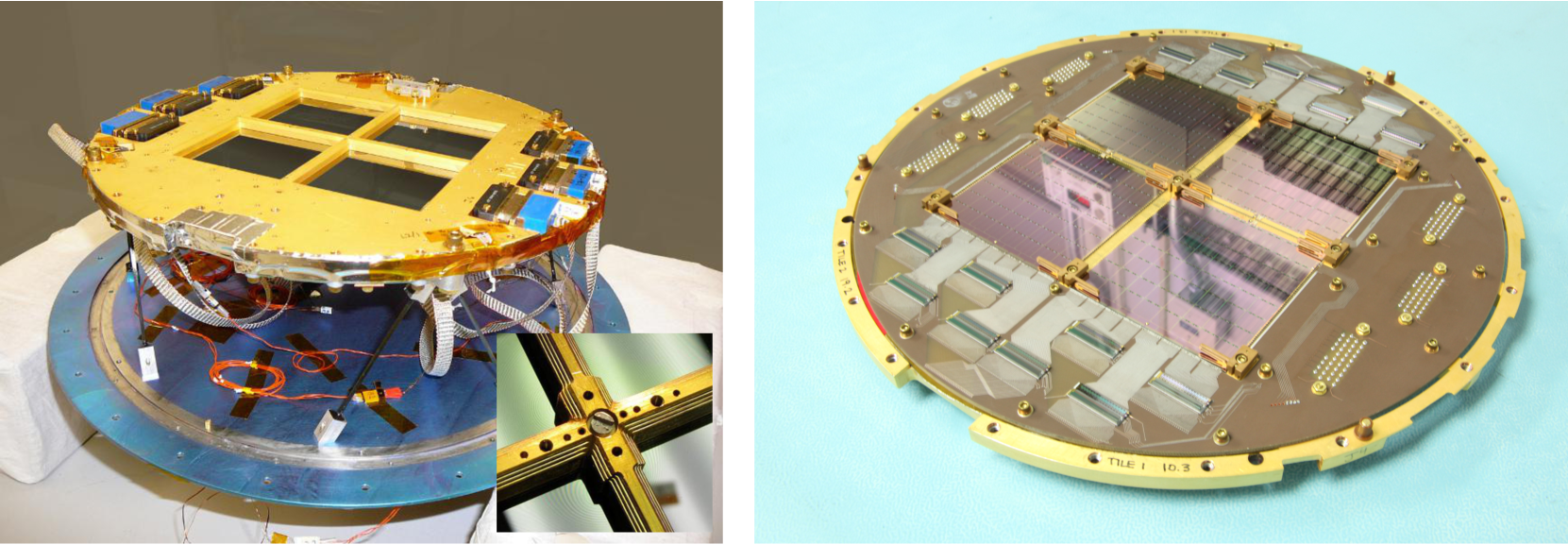
Each focal plane (Figure 1) contains four detector tiles mounted to a common copper frame. Each tile is a square of silicon cut from a standard 100 mm wafer, typically 550 m thick. The 150 GHz Bicep2, Spider, and Keck Array focal planes contain four tiles, each consisting of 64 dual orthogonally polarized detector pairs, providing 512 detectors per camera. The detectors’ beams terminate on their camera’s cold stop at -15 dB of the main lobe with spacing. The 95 GHz Keck Array cameras have tiles containing 36 orthogonally polarized detector pairs, and thus 288 detectors per camera. These detectors’ beams terminate on their camera’s stop at -12 dB of the main lobe with spacing. Current 220 GHz focal planes contain four tiles of 64 detector-pairs each in order to match a readout system designed for the 150 GHz cameras; this under samples the focal plane ( spacing), which will be addressed with a future higher density focal plane design. The 220 GHz detectors’ beams are similar in size to the 150 GHz beams, terminating on the stop at -15 dB.
We mount the tiles to the aforementioned gold-plated copper frame and thermally sink the tiles with gold wire bonds linking the frame to gold bond-pads that directly contact the silicon substrate of the tile. The antennas are patterned on the non-illuminated side of the wafer, so that light arrives at the antenna through its silicon substrate (see §3.1 for elaboration). A quartz anti-reflection tile is mounted on the illuminated side of the wafer, while the antenna side faces a superconducting niobium reflective back-short placed away. Testing of early Bicep2 prototype focal planes suggested that near the tile edge, antennas for one of the two polarizations may couple to the frame, yielding elliptical beams in the far field. We have mitigated this coupling in all deployed focal planes by keeping the edge detector pairs a few wavelengths away from the frame and by corrugating the frames with specifically chosen depth and impedance grooves, optimized with simulations performed in the CST Microwave Suite (Corp, 2009a).
Polarized Detector Elements
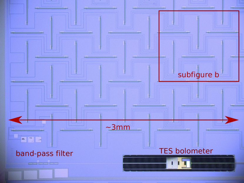
Our detector design is entirely planar and does not require horns or other contacting optics. In each detector element, optical power couples to two co-located, orthogonally polarized planar antenna arrays, each composed of slot sub-radiators patterned in a superconducting niobium (Nb) ground plane. All slots of a given orientation are coherently combined through a microstrip summing tree to synthesize a single equivalent antenna for that polarization orientation. Power from each antenna is passed through an on-chip band-defining filter before being dissipated on a suspended bolometer island. A superconducting TES on that island detects variations in the power received by the antennas.
3. Detector Design
3.1. Antenna Design
The antenna slots in each detector must be spaced to Nyquist sample the focal plane surface to avoid grating lobes that would rapidly change the impedance with frequency (Kuo et al., 2008). The antenna pattern of each axis of an array is calculated from the elements per linear dimension spaced at distance as follows:
| (1) | |||||
where is the free-space wavelength, the relative permittivity of the surrounding medium, and the sum is across sub-antennas indexed by . In addition to the strong peak in the normal direction (), there are grating lobe peaks when is a positive integer. To avoid these lobes, the slot spacing must be
| (2) |
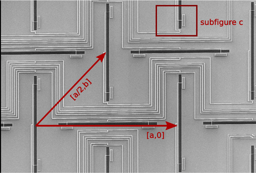
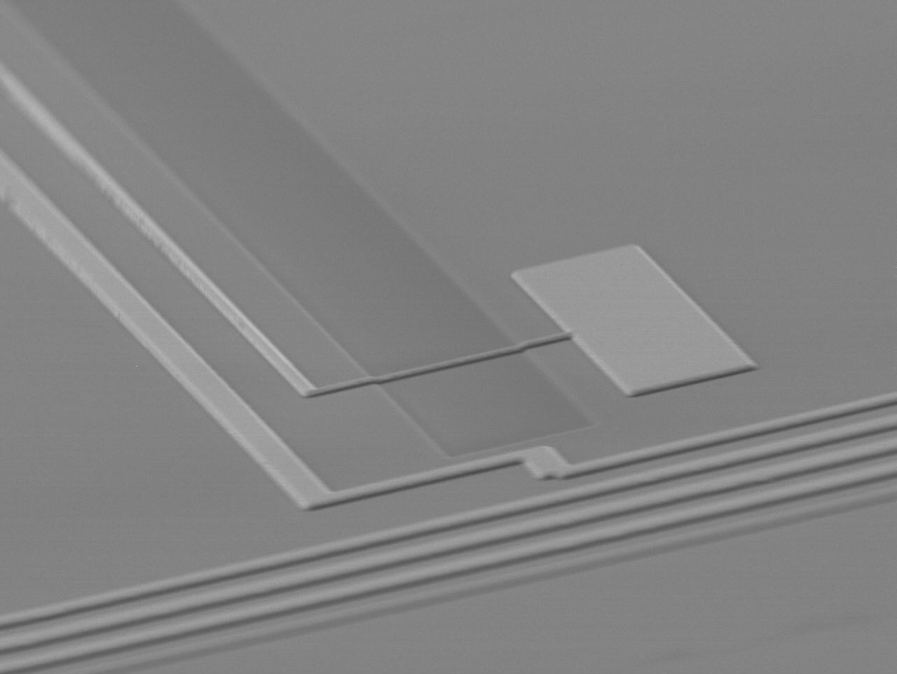
where is the minimum wavelength of operation and the term in parentheses accounts for the finite width of the grating-lobe peaks. For the 150 GHz detectors fabricated on silicon () with an upper band edge of 180 GHz (), the spacing must satisfy . To achieve this high density of radiators without intersection, we couple power to offset (echelon) pairs of radiators with a Bravais lattice defined in Figure 2. These dual-slot sub-arrays tile the detector elements in , , or versions, where the overall detector size is chosen to match the /2.2 camera optics. By using such a large number of sub-antennas, we avoid excessive excitation of substrate modes that might degrade the detector’s efficiency. The offset slot-pair geometry allows the two orthogonally polarized antenna arrays within each detector pair to be co-located (visible in upper two panels of Figure 2).
It is energetically favorable for the antennas to receive power through the silicon substrate to the vacuum side at a ratio of , where (in equation 4) differs from silicon’s TEM impedance of in phase because standing waves in the substrate modify the effective impedance seen by the slots. We exploit this power difference by orienting the tiles with the silicon substrate side towards the sky and then terminating the back response on the vacuum side with a /4 back-short. We mount /4 quartz anti-reflection (AR) tiles to minimize reflection at the air-substrate interface.
3.2. Antenna Impedance
Optical power couples from the slots to a microstrip feed network. To minimize return loss at this interface, we need to accurately compute the input impedance of that feed network. We have written custom software that provides increased speed and versatility for this task over commercial options.
We compute the input impedance of our antenna from the required jump-discontinuity in magnetic fields across the slot at the microstrip feed-points () where we impose a driving current . Modeling the currents in the ground plane with fictitious magnetic currents running longitudinally down the slot, the field jump-discontinuity requires:
| (3) |
The antenna impedance can be inferred once these currents are solved for. The Green functions describe the fields on either side of the slot () resulting from an infinitesimal magnetic current in the x direction (parallel to the slot.) In the spectral domain, these have the form
| (4) |
where and (Das & Pozar, 1987). The dielectric films support transverse electric (TE) and transverse magnetic (TM) modes with different impedances. The impedance of each mode “seen” by the slots can be computed by solving for the standing waves of electric and magnetic fields in a manner analogous to treating the silicon substrate and quartz AR coating as transmission lines and then transforming the impedance of free space () through them. (Das & Pozar, 1987) The backshort (ground) transforms through a quarter-wave space, presenting a parallel impedance that is open at the band center. The silicon substrates are a standard 100 mm diameter thick wafer, and we optimized the 95 GHz and 150 GHz impedance matching with this thickness in mind. The 220 GHz versions are fabricated on thinner thick silicon substrates to scale this design.
We expand the unknown fictitious currents in a one-dimensional piecewise sinusoidal basis (Kominami et al., 1985):
| (5) |
localized in physical space at position over the slot, with sections of length and width corresponding to the slot width. This basis models the expected current distribution on the shorter slot dimensions, leaving the unknown distribution only on the longer dimension. Moreover the Fourier transform of the basis function has a compact analytic form. These features greatly simplify the computations. Solving Equation 3 with a Galerkin moment method reduces it to a matrix equation (Kominami et al., 1985), where
| (6) |
The inverse of the admittance matrix in Equation 6 is an impedance between basis functions. The self and mutual impedance between basis functions located at feed-points is the input impedance that our feed-lines must match.
We avoid complicated numerical integration and further reduce the number of unknown s by assuming the arrays are infinite in extent and applying periodic boundary conditions where the antenna properties repeat for spectral translations along the lattice vectors:
| (7) |
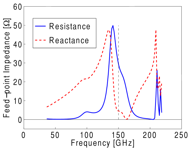
where and are the distances between the slots in the horizontal and vertical axes (see Figure 2). This approximation is valid for slots in the interior of the array and reduces the integrals to a discrete sum that we terminate at a wavevector high enough to allow convergence. Figure 3 shows the computed input impedance against frequency for the 150 GHz antennas. The oscillatory behavior at 200 GHz is expected and real (i.e. not a numerical artifact) and coincides with the onset of grating lobes. We note that we have performed more numerically intensive simulations of finite slot arrays where continuous integration retains edge effects to some degree and these agree well with the infinite array approximation.
We couple power to microstrip lines at the points near the slot ends where the lines cross and shunt to the ground-plane on the opposite side (see lower panel of Figure 2). This coupling effectively transmutes the electric fields across the slot into fields between the microstrip conductor and ground plane, provided that impedances are well matched. To avoid grating lobes, we keep the slots as short as possible and excite the slots at their first resonance. However, the radiation resistance of center-fed slots at this resonance is nearly 300 , caused by a current node at the slot center. By symmetrically feeding the slots with a pair of off-center microstrip lines close to the current anti-nodes, we greatly reduce the radiation resistance to . The microstrip feed lines must match this real antenna resistance, which, for our dielectric and metal film thicknesses, corresponds to the thinnest lines that we can reproducibly fabricate. The feed points also have a inductive reactance, which is relatively stable over the band. We tune this away with series capacitors that shunt current to ground (also visible in Figure 2). Future designs may use more complicated terminations (e.g., open stubs) in lieu of capacitors to expand the bandwidth, allowing for co-located dual-color detectors.
3.3. Microstrip feed
The waves from the slots coherently sum in the microstrip feed-network, which accomplishes beam synthesis in lieu of a horn. Figure 4 summarizes this topology. This network combines waves across rows, and then sums the waves from each row in a column tree at the side of the detector element, presenting a single microstrip line in each polarization. The two orientations of slots couple power to two independent feeds that tightly interlock across the detector pair. The feeds are meant to be corporate, combining all waves with uniform phase, but the trees are not necessarily binary. In fact, the 220 GHz and 150 GHz detectors have a array format while the 95 GHz ones are , neither of which is a power of 2.
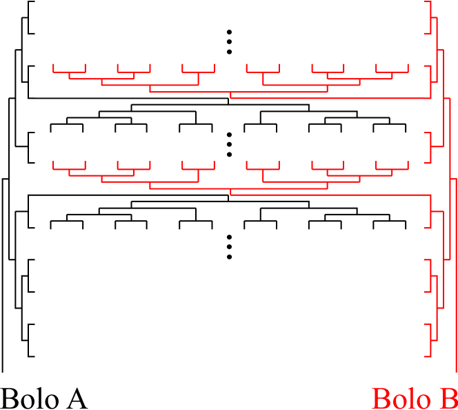
Waves sum in microstrip tee-junctions, with impedances chosen to match across each junction when looking from the port closest to the bolometer. We pick the ratio of impedances on the ports closest to the slots to determine the illumination pattern. To accomplish this synthesis with low return loss, we must construct microstrips with correct impedances, which requires accurate knowledge of dielectric constants and the penetration depth into our superconducting niobium films. (See §5.) Thus far, all detectors deployed for Bicep2 Keck Array and Spider produce a uniform top-hat illumination where the power splits are in proportion to the number of slots on each side of the junctions. The microstrip impedances can be chosen to synthesize an arbitrary pattern, however, and Gaussian tapered feeds have recently been deployed in the Bicep3 camera.
Coupling between microstrip lines can generate phase errors across the antennas, which we elaborate on in §6. The present designs have judiciously spaced the adjacent lines to minimize this coupling. To negate any residual phase errors, the feed-networks also contain sections of transmission line before each slot whose length we can vary during fabrication.
3.4. Band-defining filters
Each microstrip feed contains an integrated band-defining filter between the antenna feed and bolometer. We use a three-pole design as a compromise between bandwidth and loss: additional poles would let us increase the bandwidth and still avoid atmospheric features, but the additional passes of the waves through each resonator increase filter loss. Figure 5 shows a micrograph of the filter and a schematic of its equivalent circuit. We realize the resonators with lumped components, which do not suffer from the high frequency resonant leaks present in and transmission line resonators.
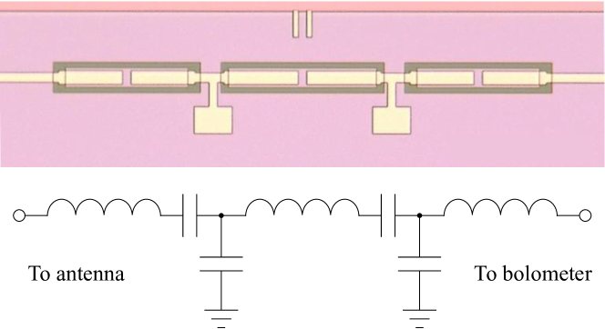
Each pole is a series LC resonator, in which the inductors are short stretches of high-impedance coplanar waveguide (CPW). The CPW impedance of roughly exceeds the surrounding lines and acts as a series inductor by allowing strong magnetic fields in the CPW ground-plane gaps. This inductance is almost entirely magnetic; kinetic inductance from the niobium superconducting microstrip and ground layers only makes a minor correction. The series capacitors are parallel-plate metal-insulator-metal between upper and lower niobium films using the microstrip SiO2 as the dielectric. In an ideal design the central resonator would be a parallel LC resonator shunting to ground. For ease of fabrication we instead build a series resonator and invert its impedance on resonance using shunt capacitors to ground and reduced series capacitors (Galbraith & Rebeiz, 2008).
We numerically optimize the filter in simulations with the commercially available Sonnet software (Corp, 2009b). The optimizations are constrained to maintain an entrance impedance of which results in fabricable capacitors and inductors. Our design results in inductors longer than that have some slight parasitic shunt capacitance, but this does not degrade the performance appreciably. The filter in Figure 5 is tuned for a 150 GHz band-center. Filters for 95 GHz and 220 GHz versions have components with the same reactance at the resonant frequencies. We show spectra and summarize spectral response features in §7.
3.5. Bolometer Design
We terminate and thermalize millimeter-wave power on a released bolometer island in a meandered lossy gold microstrip. 150 GHz waves are constrained to propagate through a skin depth of , and over a length of several wavelengths the line absorbs 99% of the power between two passes. We scale the 220 GHz and 95 GHz designs appropriately to maintain dB return loss.
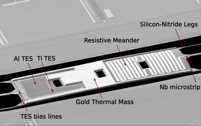
This termination is in close thermal contact with two transition edge sensors: an aluminum TES with a transition temperature for lab tests and a titanium TES with a for on-sky observations. The saturation power (optical plus electrical power) needed to bring the TES temperature to is
| (8) |
where the conductance is evaluated at the transition temperature and the surrounding heat bath is . The exponent reflects the thermal carriers in the legs, where would correspond to electrons and would correspond to phonons in 3-D materials. Our typical devices are described by . The aluminum affords the bolometer a high saturation power for use under a 300 K background, but has higher noise that would be unacceptable for astrophysical observations.
Each bolometer island is suspended from the tile by six isolation legs: one carrying the microstrip from the antenna, one carrying the TES DC lines, and four thinner legs for mechanical stability. Some newer devices use four legs, while Spider employs long meandered legs as described below. We tune the bolometer legs to achieve the design thermal conductance. We aim to keep the phonon noise subdominant to the photon noise, but also to keep the high enough that the detectors do not saturate under typical on-sky loading conditions, which for Bicep2 is –. We typically build in a safety factor of 2 beyond the expected maximum loading; for Bicep2 this resulted in –, as described in §7. Two detector pairs in the corners have the microstrip opened between the antenna and bolometers such that the TESs do not receive optical stimulation through the microstrip feed. As described in §6.3, we use these four bolometers for diagnostic measurements and to monitor direct stimulation of our detectors by optical power that bypasses the microstrip circuitry and may thus not have the required spectral and polarization properties.
Thick evaporated gold (visible in Figure 6) is added to the bolometer islands to boost the heat-capacity by , bringing the time constant to around a millisecond. We infer this from responses to a 1 Hz square-wave modulated broad-spectrum noise signal. The additional gold is important because of the strong electrothermal feedback of these devices; without it, our detectors would enter electrothermal oscillations throughout much of the TES transition.
We voltage bias the TESs into the transitions typically at half the normal resistance (i.e. ), using parallel shunt resistors. We detect changes in the TES current using a SQUID-based time-domain multiplexing architecture, where all detectors in a set of 32 are sequentially read through a common set of lines (de Korte et al. (2003) and Stiehl et al. (2011)). For Bicep2, our revisit rate of a given detector is , ensuring that we Nyquist sample the time-stream up to the 6 kHz roll-off imposed by a series inductor.
Adapting this technology to the low photon loadings of Spider’s long-duration balloon payload poses challenges in detector and instrument design. In order to take full advantage of the low photon noise levels available at 36 km altitudes, care must be taken to ensure that the bolometers achieve low noise levels and the surrounding instrument contributes minimal additional photon loading.
Spider employs several modifications to the Bicep2 detector design to reduce detector noise. A meandered leg design reduces conductance to pW/K, reducing phonon noise while remaining within a similar footprint. This chosen is not limited by the anticipated loading of but rather to have margin on the 300K background in the laboratory while biased on the Al TES. Lower leads to naturally slower detectors, reducing the need to add heat capacity to the island with thick gold (Au) to maintain stability. The long cabling in Spider prevents us from multiplexing faster than kHz, so we control aliasing with larger inductors.
4. Fabrication
We fabricate detectors in monolithic batches of 64 matched pairs at the Microdevices Laboratory (MDL) at the Jet Propulsion Laboratory (JPL). We fabricate arrays on – thick silicon substrates chosen for optimal optical coupling. We deposit – low-stress silicon nitride films (LSN) and tune the internal stress to be as low as 150 MPa to ensure mechanical integrity.
| Material/Function | Deposition | Etchant |
|---|---|---|
| 1. Low-stress nitride | High temp LPCVD | CHF3 ICP-RIE |
| 2. Aluminum TES | e-beam evaporation | Liftoff |
| 3. SiO2 Pro-1 | RF sputtered | ICP, CHF3/O2 etch |
| 4. Titanium TES | sputtered | ICP, Freon-1202 |
| 5. SiO2 Pro-2 | RF sputtered | ICP, CHF3/O2 etch |
| 5. Niobium Ground Plane | Magnetron sputtered | Liftoff |
| 6. SiO2 ILD | RF sputtered | ICP CHF3/O2 etch |
| 7. Gold resistor | e-beam evaporated | Liftoff |
| 8. Niobium Microstrip | sputtered | ICP, Freon-1202 |
| 9. Gold heat capacity | e-beam evaporated | Liftoff |
| 10. Silicon release | substrate | STS DRIE/ XeF2 |
| *Acronyms defined in text |
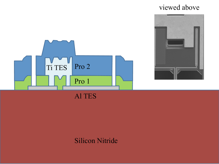
The TES normal state resistance and transition temperature are sensitive to thickness variability and chemical contamination, so we deposit and pattern our TESs before the millimeter wave circuitry on a flat and chemically clean surface. We first e-beam evaporate aluminum (Al) and pattern the TES. We DC-sputter titanium (Ti) and use inductively coupled plasma (ICP) etching to etch the TES for on-sky observing. Both films are immediately chemically passivated with RF-sputtered silicon dioxide () with ICP etched via holes to allow DC electrical contacts with subsequent layers. The RF bias ensures that the passivation patches have rounded edge walls so that subsequent films can make contact over steps. The top panel of Figure 7 illustrates these first steps. The Al and Ti films make a series DC connection and are later connected to Nb bias lines.
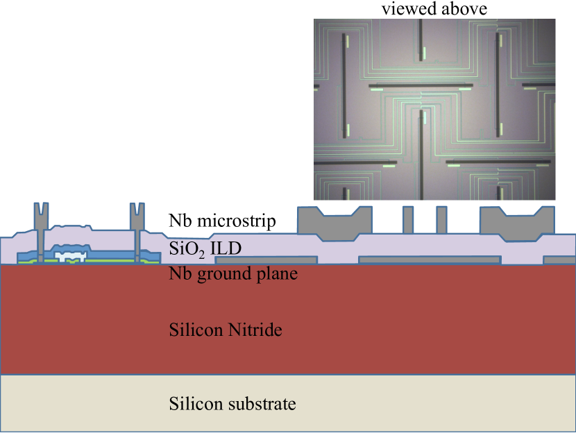
The millimeter wave circuits are fabricated from four films: a niobium ground plane, a interlayer dielectric (ILD), an upper microstrip Nb conductor, and thin Au resistive termination. We DC-sputter the Nb films and pattern the ground plane with lift-off, a technique where we first deposit photoresist and then dissolve it from under the metal film to be removed. In principle, this film could be etched, but we suspect that the Ti can be altered by this step despite the intervening protect layer. The Nb ground film defines the antenna slots, bandpass filter inductors, holes for bolometer release, and safety holes under the bond-pads. This film also fills the bias vias down to the TESs. Lift-off provides rounded side-walls and thus ensures step-coverage of subsequent films. The Nb ground-plane covers more than 90% of the 100 mm wafer, serving as both the DC and RF ground for the detector array.
We have explored several ILD materials, although all currently deployed devices use RF-sputtered silicon dioxide. Thickness uniformity of this film is crucial for detector uniformity across the array. A 6 inch SiO2 RF sputtering target and substrate rotation help achieve thickness uniformity to better than 7% across the array. We use an inductively coupled plasma (ICP) reactive ion etch system to etch release holes around the bolometers and vias that allow for a DC connection to the buried TES structures in the subsequent Nb metallization fabrication step.
We form the resistive terminations on the bolometer islands with e-beam deposition and lift-off patterning. Finally, we DC-sputter the upper Nb microstrip conductor and etch from that film the microstrip feed network, band-defining filter capacitors, and DC bolometer bias lines and bond-pads using a freon etch. We have found that lift-off techniques (used for Bicep2) and chlorine-based (BCl3) etches can contaminate the Nb films at this step, resulting in unacceptable millimeter wave losses in our circuitry as discussed in §5 and §6.2. The middle panel of Figure 7 illustrates these intermediate microwave steps that define ground plane, ILD, and microstrip traces.
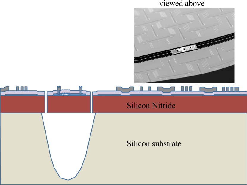
The final fabrication steps release the bolometer islands, illustrated in The bottom panel of Figure 7. We etch through the LSN with in an inductively coupled plasma reactive ion etch ICP-RIE system, exposing bare silicon under the release holes. We e-beam evaporate and lift-off thick gold onto the islands to add heat capacity and control the required readout bandwidth. We use an STS deep reactive ion system to etch from the front side and remove silicon from the release holes. This Bosch etching process uses a combination of etching and passivation steps to cut vertically through the silicon wafer, after which we undercut the bolometers with a XeF2 release (Turner et al., 2001). XeF2 attacks the remaining exposed silicon isotropically, so the small hole pattern in the photoresist is pre-determined to release only the islands and legs and to not undercut the remaining antenna structures. Finally, we use the STS etcher to cut out the square tile with holes for alignment pins. Table 1 summarizes these fabrication steps.
5. Material Properties for the millimeter wave circuits
We separately characterize the material properties used in the design of the antenna feed and filter, in particular the Nb penetration depth and the ILD dielectric constants. These material parameters are poorly characterized in the literature for millimeter waves, and they can depend on details of the processing. We also need to characterize loss properties and monitor stability over time. To address these concerns, we have fabricated companion tiles of test devices where each detector pair receives power through a single polarization broadband integrated antenna. The microstrip feed evenly divides power in a microstrip tee-junction between a device under test (DUT) and a reference bolometer to divide away optical effects from the antenna and fore optics. We measure the spectral response of the bolometers through Fourier transform spectroscopy (FTS) with a Martin-Puplett interferometer (Martin & Puplett, 1970), combining the detector time-streams and encoder readings from the moveable mirror’s translation stage to form interferograms. We low-pass filter, zero-path difference, and Hanning apodize the interferogram before Fourier transforming the interferogram into the frequency response .

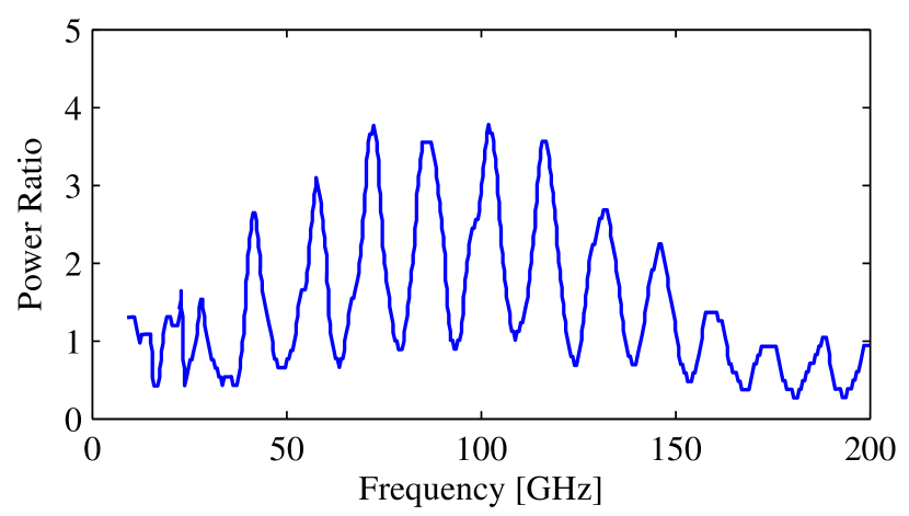
We use one device for microstrip wave speed measurements. The DUT is a microstrip Fabrey-Perot cavity with an impedance intentionally mismatched from the surrounding lines. The standing wave pattern in the spectrum of the bolometer behind the cavity can be used to determine wave speed. (See Figure 8 for a schematic and data sample.) The wave speed is a function of both the ILD dielectric constant and the Nb penetration depth . Alternatively, the band-defining filter resonance is determined by series inductance dominated by the CPW magnetic inductance. Data from the band locations and test devices allow us to solve for both and and we summarize these numbers is Table 2 for different materials.
| Parameter | Value |
|---|---|
| SiO2 | 3.9 |
| SixNy | 7.0 |
| Nb | 0.1 m |
Another test device measures loss per length in our transmission lines, where the device under test is a stretch of line that is several wavelengths long. We determine loss as a function of frequency by forming the ratio of FTS spectra seen through the long line and the reference bolometer. While the loss tangent has been shown to be dominated by loss in dielectrics, and can be quite low in some dielectric systems, our measurements determine loss in the microstrip as fabricated. Thus far we have tested PECVD SiO2, PECVD SixNy and evaporated SiO2 in this manner.
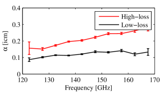
This loss test capability became particularly important during a period of time when the optical efficiencies of our fabricated devices were unusually poor. This test program allowed us to show that the effective loss tangent of our microstrip had a frequency dependence (see Figure 9) when using all three of the dielectrics above. This common problem present with three ILDs from different deposition systems suggested that the loss was generated in the Nb films. Ultimately, these measurements helped us to identify and correct a modest tensile stress in the Nb as deposited by sputtering. Further, the loss appears to be sensitive to the reactive ion etch chemistry used in the Nb process. Controlling the film stress at a nominal compressive -100 to -300 MPa and changing the Nb etchant from BCl3+O2 to Fl2+O2 resulted in lower loss tangent with a dependence (see Figure 9).

6. Beam synthesis
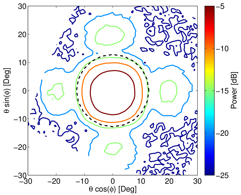
The antenna array combines waves from the sub-antennas with equal amplitude and phase to synthesize a uniform illumination, which generates a sinc pattern in the antenna far field. Using a test cryostat, we characterized the antenna far field pattern and confirmed that the antenna has a beam waist of 4.1o () and side-lobe level of -12 dB relative to peak response, as expected from the design. A sample far-field pattern is shown in Figure 10, taken in a cryostat without lenses or a stop. For a detailed beams characterization in the complete Bicep2 and Keck Array cameras, we refer the reader to the Bicep2 and Keck Array Beams Paper (Bicep2 Collaboration IV, 2014).
Our ground-based experiments difference detector pairs at the time stream level to suppress unpolarized common-mode noise from the atmosphere. However, differencing at this early point in the analysis pipeline can allow temperature anisotropies to leak into polarization if the detector beam patterns are mismatched. This is an especially acute challenge to small aperture experiments because the beam size couples to large temperature gradients at degree scales.
Our team has developed an analysis technique, called deprojection, that discards contaminated modes. As described in the Bicep2 Systematics Paper (Bicep2 Collaboration III, 2015), the pipeline can remove temperature leakage through relative-gain mismatch (monopole moment of beams), first derivatives of temperature through displaced centroids (dipole moment of beams), and second derivatives of temperature through differential beam widths and ellipticities (quadrupolar moments of beams).
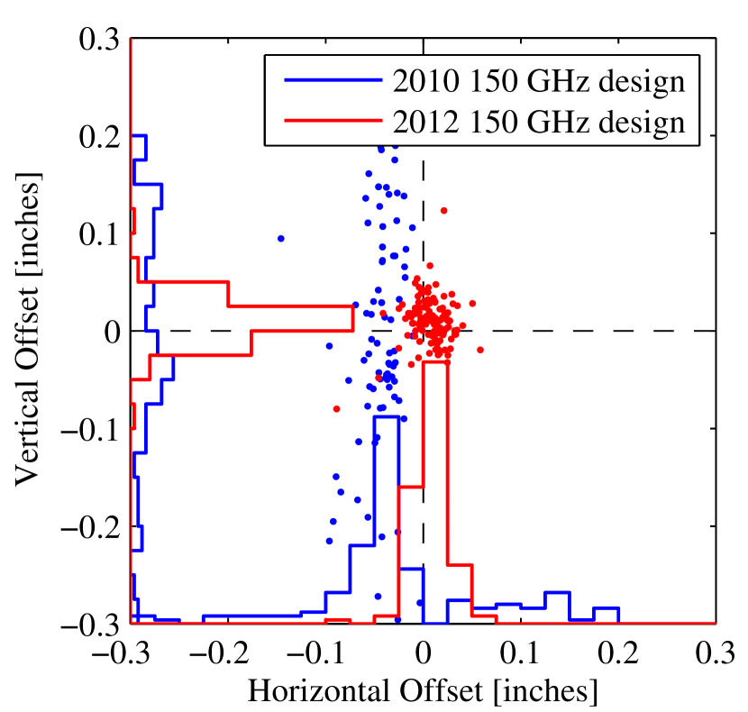
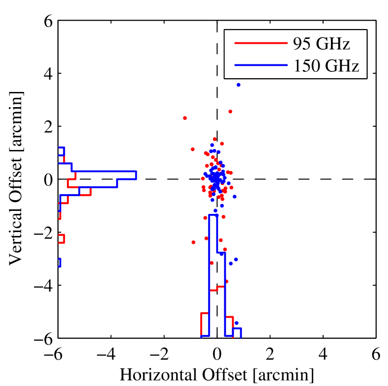
The detector design is most prone to centroid displacement, as characterized in the Beams Paper (Bicep2 Collaboration IV, 2014). We have identified two mechanisms responsible for beam displacement and implemented design and fabrication fixes to suppress their contamination below the level (O’Brient et al., 2012). These fixed detectors are deployed in Keck Array and Spider and Figure 12 shows the centroid steer before and after these corrective measures.
6.1. Parasitic microstrip cross-talk
The microstrip lines in the feed networks’ horizontal arms must fit between the slot sub-radiators, crossing them only at the intended feed points. To achieve this, the lines must be in close proximity, and for the 150 GHz Bicep2 devices, many lines are separated by only 10 dielectric thicknesses. This separation would be adequate to avoid cross-talk for short stretches of lines, but some of the line pairs run parallel for over four wavelengths. The longest of these pairs are those running from the sides to the center to begin the horizontal tree arms, coupling power to one of the two lines they intentionally split power between, as seen in Figure 4 and summarized in the bottom of the left panel of Figure 11.
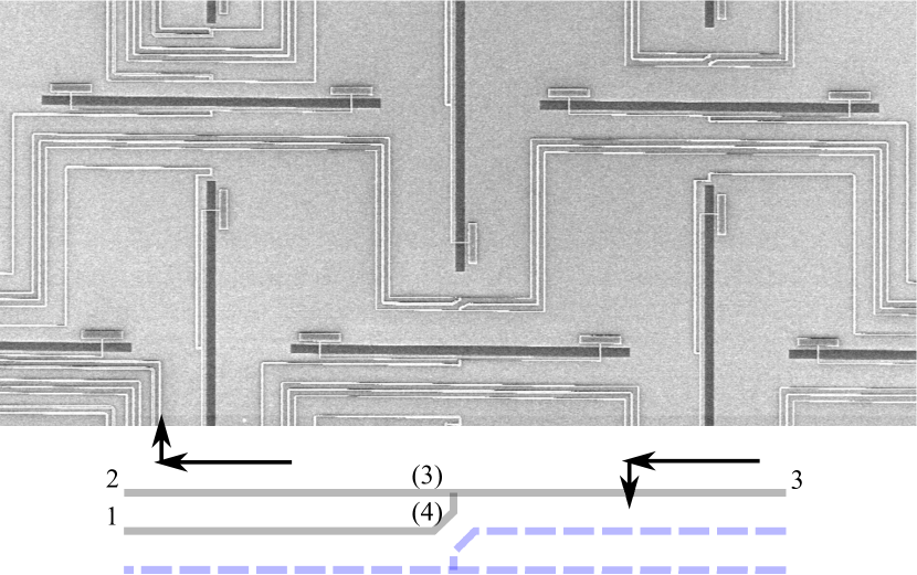
In a reverse-time picture, power from port 1 (defined in Figure 11) should be evenly divided between ports 2 and 3. The currents in a pair of parallel lines can be expressed as a superposition of even and odd modes, where the even mode has the same current magnitude and directions in each line and the odd mode has the same magnitude but opposite directions. Coupling between the two parallel lines, however, results in the two modes having different field concentrations in the air and dielectric volumes, and so induces a difference in wave speeds between the modes. Waves passing from port 1 to internal port (4) thus also couple waves into internal port (3) that lag by 90∘ in phase:
| (9) | |||||
where and are the even and odd mode wavenumbers and is the parallel coupling length. This circuit acts as an unintentional reverse-wave coupler, where impedance mismatches between even and odd modes are small, but wavespeeds are not (Hammerstad & Jensen, 1980). The waves entering the microstrip tee-junction from internal port (4) add in quadrature to the intended waves from internal port (3), advancing the total phase on the side opposite the vertical tree and retarding it on the other. This phase-step steers the beams off boresight away from the vertical summing trees and is where the left-right symmetry splitting occurs in the feed. This effect produces the repeatable horizontal centroid steer seen in the cameras’ near field. We have reproduced this in simulations using HFSS that account for the upper conductor finite thickness.
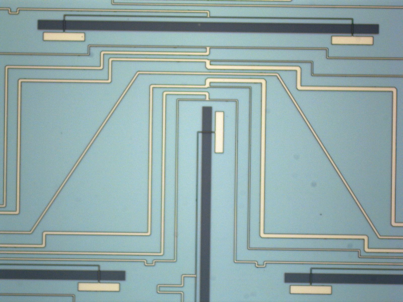
As seen in the right panel of Figure 11, we have re-designed the antenna feeds for the Keck Array and Spider detectors to greatly increase spacing between the lines and therefore reduce the parasitic coupling effect. We also include adjustable phase-lag lines before each slot to remove residual phase-error and to synthesize matched beams, although the current antenna-feeds’ increased spacing renders the corrective phases unnecessary. These phase-lags are visible in the bottom of the right picture in Figure 11.
6.2. Niobium contamination
Magnetic fields can penetrate into a superconductor by a characteristic depth . Impurities in niobium films scatter Cooper pairs with a mean free path , increasing the penetration depth beyond the London depth of pure niobium to , where is the Cooper pairs coherence length. As displayed in Table 2, our films are typically measured to have , suggesting mean-free path of , well within the “dirty” limit where film cleanliness can impact circuit performance.
Nonuniform contamination can produce nonuniform kinetic inductance, which can spatially perturb the wavespeeds in the microstrip summing tree. Variations in wavespeed can steer beams off boresight. Additionally, the summing tree does not treat the two polarizations identically, and as a result, they can be steered differentially. We have observed that the tiles with the largest scatter in beam centroid position correspond to those with the largest vertical dipole components. We also expect the tree to induce larger steering in the vertical than horizontal because slots along rows combine immediately in the horizontal tree, resulting in less integrated phase error than those along columns that combine in the vertical tree after horizontal summing.
We have built models for how our antenna-feeds perform with film gradients. We subdivide the circuit into short sections of transmission lines and tee-junctions and use each section’s location in the detector to assign unique film properties. We construct simple scattering matrices for each section and cascade them into one large matrix per polarization(Bodharamik et al., 1971). From this we can compute slot illumination patterns and thus far-field patterns. We find that 20% variations in across the array can produce differential pointing that is 10% of the beam FWHM in the vertical directions, and half that on the horizontal, similarly matching our observed scattering in pointing.
We defined our microstrip lines in early tiles with the lift-off technique that we use for the Nb ground plane, as described in §4. Several devices have shown discoloration in this step, leading us to speculate that the Nb leaches organic materials from the resist during lift-off. These observations and modeling inspired a switch to an etch-based means of defining the Nb microstrip lines (described in §4). This simple fix reduced the scatter in centroid location to % of Gaussian width , and the right panel of Figure 12 shows the centroid alignment between polarization pairs for both colors of deployed focal planes.
6.3. Direct stimulation of bolometers
Optical power is meant to reach the bolometers only through the antenna and microstrip feed network. However, photons can directly excite responses in the detectors which is of particular concern in a design where there are no horn blocks to shield the sensors themselves. In Bicep2 pre-deployment testing of early generations of detectors, response to out-of-band power was detected at levels 3%-4% of the total response, with near field and far field angular response patterns consistent with direct stimulation of the bolometer islands. Simulations in HFSS and CST suggest that the ground plane on the bolometer islands can be inductively held at a different voltage than the surrounding ground plane through the microstrip ground that we deposited only on one leg in early generation prototypes. This voltage can drive millimeter-wave currents through the gold-termination, resulting in a direct stimulation of the detectors not through intended antenna and microstrip feed. Steps taken prior to Bicep2 deployment to minimize this coupling included the addition of metal mesh low-pass edge filter above the focal plane and several design changes to the bolometer islands themselves. The island leg design was modified to narrow the width of the opening in the ground plane surrounding the island, and ground plane continuity was extended onto the island by metalization of the four outer support legs.
With these modifications in place, we have taken Bicep2 and Keck Array 150 GHz camera optical efficiency measurements with and without high-pass “thick-grill” filters that obstruct power below 200 GHz; after accounting for the filter’s filling factor, we found that the optical response through the filter was % of that without filtering. This small leakage suggests limited “blue-leaking” that would allow above-band power to excite response in the bolometer. We have also measured the response of our detectors to a chopped thermal source on boresight through a polarizing grid at different angles; we have found that the crossed response is similarly % of the co-polarized response, consistent with known multiplexer cross-talk levels. If the detectors are acting as a direct absorber, then their small area compared to the antenna’s should provide a broad angular response. As a result, we expect that the stop in the cameras for these experiments helps limit the direct stimulation and we have found that tests of devices in cameras with faster optics can have higher direct stimulation levels.
7. Array properties and uniformity
Our high attained sensitivities are a result of our high detector yield, a figure that depends on attaining uniform detector properties across the array. This uniformity also helps to mitigate some potential sources of systematic error. This section describes array uniformity of a variety of properties.
7.1. Bolometer thermal conductance
Thermal fluctuation noise across the bolometer legs is the largest internal source of noise in Bicep2, and is given by:
| (10) |
where the “Mather factor” accounts for thermal gradients across the bolometer legs and varies between 0.5 and 1 (Mather, 1982). The saturation power of the detector is given in Equation 8. Note that the leg thermal conductance is a function of temperature.
The legs’ total parallel thermal conductance needs to be chosen to keep thermal carrier noise subdominant to photon shot and Bose noise, but avoid saturation under on-sky loading. We try to have the total saturation power (Joule heating from the bias circuit plus optical loading on the detectors) exceed the optical loading ( at 150 GHz in Bicep2) by a factor of two. This aggressive safety factor is only possible if we have tight control of our processing parameters that determine and (discussed in the next subsection). Our achieved repeatability between detectors in a tile and from tile-to-tile are shown in Figure 13. Our time-division multiplexing readout requires that detectors in a common readout column be commonly voltage biased (Battistelli et al. (2008) and Stiehl et al. (2011)), and our control of within a tile allows this.
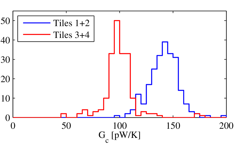
The XeF2 release only has a 10:1 selection ratio between silicon nitride and silicon, and variation in bolometer leg thicknesses from nitride etching would seriously compromise these numbers. For this reason, we oxidize the wafers prior to nitride deposition. The thin 100 nm SiO2 film has a much higher 100:1 selection ratio between oxide and silicon and thus protects the legs from XeF2 attack (Williams et al., 2003). This oxide film ensures more uniform leg cross-sections across the detector arrays, and thus more uniform bolometer s.
7.2. Transition temperature
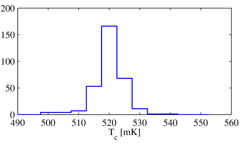
The balance between the between the internal 3He/3He/4He fridge cooling power and thermal loading lets the focal plane cool to . We use heaters to operate the focal plane at an elevated so we have margin to control this temperature through active feedback loops while still maintaining photon-noise-limited sensitivity. This choice provides the detectors with a bath temperature . For bolometer legs with n=2.5, is minimized at an island temperature of , although this is a broad-optimum with a gentle slope at higher temperatures. For on-sky operation, electrothermal feedback locks the bolometer to the titanium TES’s . While this temperature is higher than optimum, it provides some extra margin against our detectors latching into a pure superconductive state while only increasing the NEP from thermal conduction by 4%. By selecting a pure superconductor for this TES instead of a bilayer (Fabrega et al. (2009), Gildemeister et al. (1999) and Myers et al. (2005)), we obtain repeatable transitions devoid of the multiple transitions that can result from a bilayer’s complicated chemistry. Deposition on bare wafers and passivation of oxide protection layers also help maintain uniform values between and within tiles. As seen in Figure 14, our titanium is uniform across tiles and even between tiles, maintaining uniform saturation powers (Equation 8) within a multiplexer column, necessary to find a common bias point.
7.3. Normal resistance
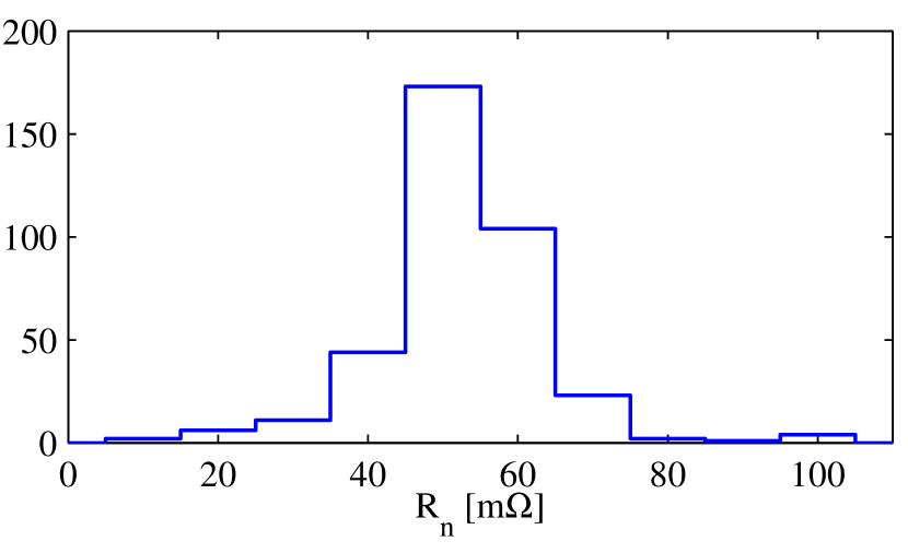
TES bolometers will only experience electrothermal feedback if voltage biased, and we bias our nominally Ti TESs with a 3 shunt resistor. The Al TES is even higher in resistance, so both are far larger than the shunt. However, this condition is only met if the Ti TES resistance is repeatably this large. We also need them repeatable in value so the detectors will have a common latch resistance and thus a common bias point where they will experience strong feedback. Figure 15 shows that these values are indeed uniform between and within tiles. Just as was true for uniformity, our recipe of a pure TES deposited as first layers on the tile, protected with an oxide film, helps maintain repeatable performance.
7.4. Time constant and loop gain
The effective thermal time constant of an ideal voltage-biased TES bolometer is given by
| (11) |
where the intrinsic bolometer time-constant is decreased by the effective loop gain of electrothermal feedback, . The responsivity of our detectors is the change in measured current for a change in incident optical power, given by
| (12) |
Both of these expressions experience corrections for non-idealities such as finite shunt resistance. Equations 11 and 12 indicate that a high loop gain will increase the speed of the sensor and simplify its responsivity (). Operating the bolometers in this limit also maintains a fast detector response (low ), giving rise to an approximately flat detector transfer function for the frequencies of interest, which for our ground-based experiments are (Irwin & Hilton, 2005).
In order to maintain stability against electrothermal oscillations, the detectors’ thermal bandwidth must not exceed that of the electrical bias circuit. The Bicep2 bias circuit includes a inductor in series with the bias resistor to avoid aliasing above a roll-off of . To limit the TES bandwidth, we deposit thick gold onto the Bicep2 detectors that adds an additional heat capacity to the bolometer island. The resulting time constants at typical science biases are shown in Figure 16.
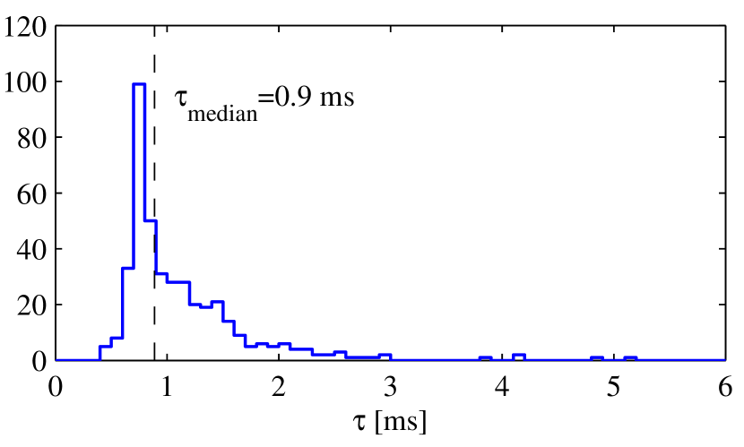
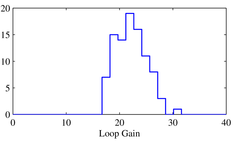
Spider detectors are intrinsically slower due to their lower leg conductance. It is thus not necessary to add as much gold to the island to ensure stability; typically only 0.5 m is deposited. Time constants on transition are found to be similar to Bicep2’s. For Spider detectors we have measured time constants in response to optical square-wave excitations at a range of bias voltages (and thus TES resistances), allowing us to infer that the normal time constants (without loop gain) are and that loop gains are at (Figure 16). Bicep2 TESs should have similar loop gains. We note in passing that fast bolometer time constants are useful for limiting the effect of particle radiation (e.g., cosmic rays) on detector time streams in balloon- and space-borne instruments.
7.5. Spectral Response
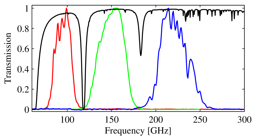
Our cameras use a series of low-pass filters, both absorptive plastic and reflective metal-mesh, to limit thermal loading on the focal plane and above-band response of our detectors. However, we rely upon the integrated microstrip filters described in Section 3.4 to avoid the atmospheric lines immediately adjacent to our observing bands. Figure 17 shows measured response averaged across a focal plane for three different spectral channels (in three different focal planes), demonstrating that this technology does indeed avoid atmospheric features.
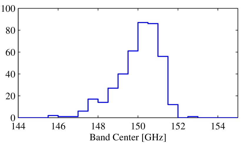
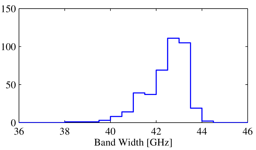
We can summarize the spectral response by comparing it to a top-hat response with the same area and then defining the band-center as:
| (13) |
and the bandwidth as
| (14) |
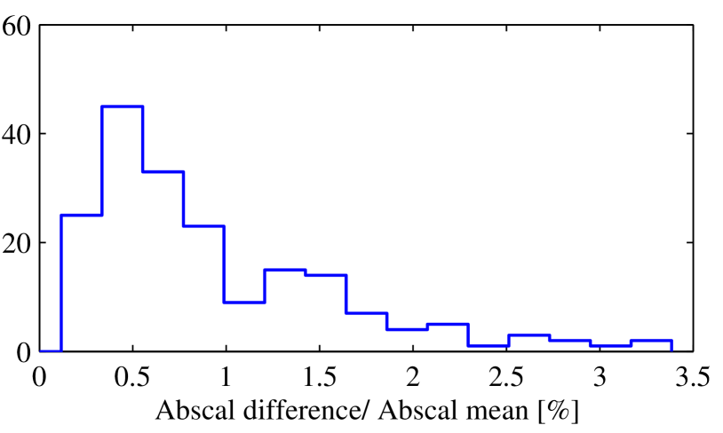
The spectral responses of the detectors within a polarization pair must be closely matched to avoid systematic contamination through spectral gain mismatch. In principle, using separate filters for each polarization might induce a mismatch through gradients in material properties. Our design resists this by placing the filter pairs in close physical proximity; in the 150 GHz detectors, the filters are 5 mm apart. Furthermore, the filters’ magnetic inductance dominates the kinetic inductance; this renders our filters’ features particularly robust against variation in Nb contamination that might adversely impact electrically long resonators (Myers et al., 2005). As shown in Figure 18, our band centers and widths are found to be highly repeatable. We calibrate our responsivity through correlation against the Planck 143 GHz maps. Spectral mismatches between filter pairs would manifest themselves as differences in each detector’s absolute calibration (abscal), but the bottom panel of Figure 18 shows that these are less than 3% of the average responsivity, with a median of 0.5%.
7.6. Optical Efficiency
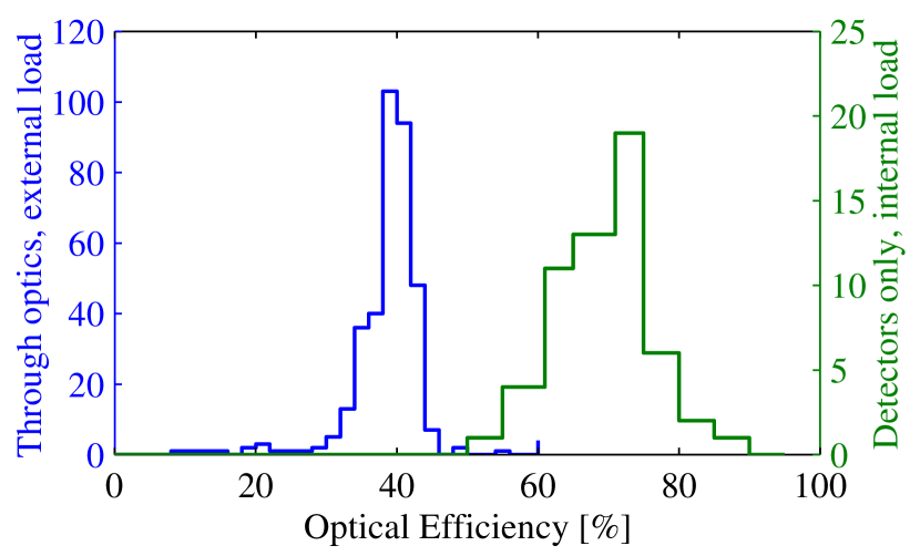
We characterize our end-to-end optical efficiency by biasing onto the aluminum TES, which has a higher than Ti, and thus higher saturation power. By comparing the measured response to aperture-filling 77 K and 300 K sources to the expected incident power , we can use the measured spectra to infer efficiency. We routinely obtain total camera optical efficiencies in excess of 30%. For example, the Bicep2 efficiencies are shown in Figure 19. These figures are for the total camera efficiency, which includes losses other than the detectors. Measurements of response of early engineering-grade detectors to an internal cold load, which exclude spillover loss and loss in our filter stack, suggest that the raw detector efficiency should be nearly 70% (Orlando et al., 2009).
8. Sensitivity
The array design described above was first deployed for astronomical measurements in 2009 as part of Bicep2, a ground-based CMB polarimeter. We have since fabricated dozens of deployment-grade arrays at 95 and 150 GHz for use in the terrestrial Keck Array and balloon-borne Spider instruments. These programs have yielded extensive data on the real-world performance of this technology, as well as demonstrating its adaptability to different optical loads.
8.1. Noise
The theory of noise in TES bolometers is by now well developed (Irwin & Hilton, 2005). Major contributions typically include photon noise, phonon noise (thermal fluctuation noise), Johnson noise from the TES and shunt resistances, and amplifier noise. In many cases TESs also exhibit varying degrees of “excess” noise beyond that predicted by simplified models. In multiplexed systems, noise performance also depends upon the relationship between the noise levels and detector and readout bandwidths, since poor choices can lead to substantial noise aliasing (Battistelli et al. (2008), and Stiehl et al. (2011)). We find that the detectors’ measured noise is well reproduced by a simple model incorporating modest excess TES noise, and we have successfully operated the bolometers in configurations with little aliasing penalty.
In order to characterize the noise performance, we have measured noise spectra for the Bicep2 and Keck Array detectors using un-multiplexed data digitized at 400 kHz. Although the frequency range corresponding to degree-scale anisotropies is 0.05–1 Hz for the Bicep2 and Keck Array scan strategy, these measurements allow us to observe device performance near the typical multiplexing frequency of 25 kHz and thus model noise aliasing due to the readout. These measurements, adjusted for expected aliasing, are in good agreement with noise measured in the science-mode multiplexer configuration.
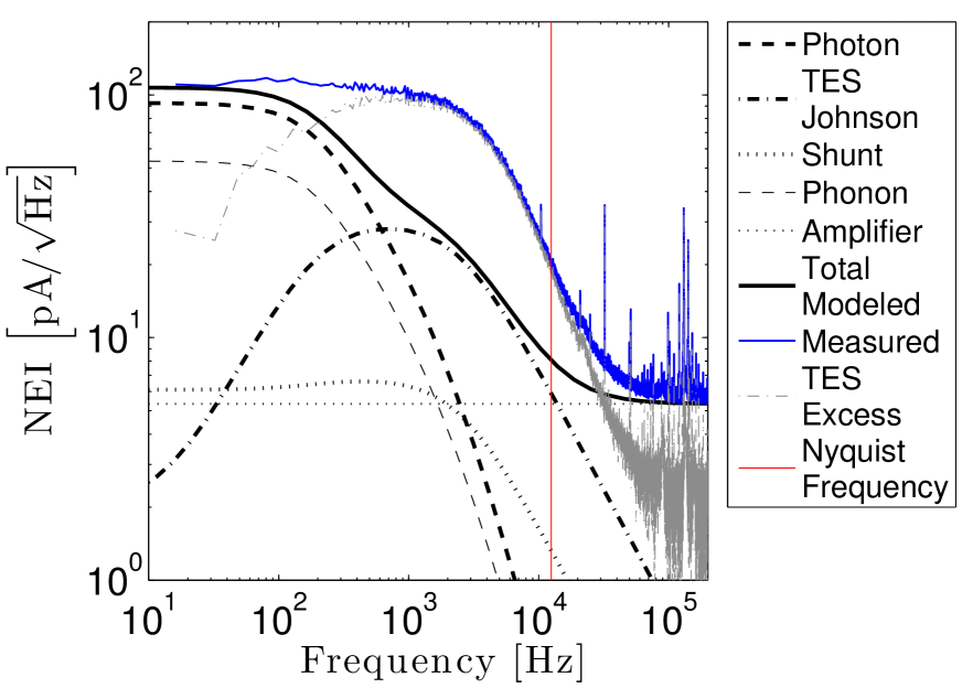
Figure 20 compares the measured noise for a representative detector from the Keck Array to its various modeled components. Photon noise dominates at the low frequencies of interest for sky observations. The photon noise equivalent power (NEP) can be expressed as a sum of Bose and shot noise contributions:
| (15) |
where is the band center, is the bandwidth, and is the optical loading. The next-largest contribution to the noise at low frequencies is the thermal fluctuation (phonon) noise across the SiN isolation legs, given by Equation 10. All other modeled contributions, including the TES Johnson and excess noise, the shunt resistor noise, and the cold and warm amplifiers, are negligible at low frequencies.
| Receiver | Bicep2 | Keck Array Rx0 | Rx1 | Rx2 | Rx3 | Rx4 |
| Absorbed Photon Noise [] | 41 | 33 | 32 | 34 | 27 | 27 |
| Phonon Noise [] | 27 | 24 | 20 | 24 | 14 | 16 |
| TES Johnson Noise [] | 0.5 | 0.8 | 0.5 | 0.8 | 0.4 | 0.6 |
| Amplifier Noise [] | 2.0 | 2.0 | 2.0 | 2.4 | 2.0 | 2.5 |
| Total Noise + Aliased at 25 kHz [] | 56 | 46 | 39 | 48 | 36 | 40 |
| per-detector NET from maps [] | 305 | 316 | 351 | 317 | 370 | 429 |
At frequencies of the TES excess noise starts to contribute significantly. The TES excess noise, as described in (Gildemeister et al., 2001), tends to be proportional to the TES transition steepness , which for these detectors is higher at lower resistances. The excess noise varies between fabrication batches, although the detector in Figure 20 has a relatively low amount. The excess noise should have little contribution to an experiment’s overall noise level as long as it is not aliased. Bicep2 and the Keck Array avoid such aliasing by multiplexing at 25 kHz and biasing at relatively high resistances on detectors that have large excess noise components. Spider cannot multiplex as quickly due to long cable lengths, so we use a lower TES resistance ( m) and higher Nyquist inductance (2.0 H) to limit aliasing of excess noise.
The noise contributions for Bicep2 and the Keck Array at low frequencies and under winter atmospheric loading conditions are broken down in Table 3 for the observing year 2012. The photon noise is of absorbed power only to aid the comparison between models and measurements without adding an extra factor of optical efficiency. The last line of the table shows total NET computed from jackknife maps, which necessarily references noise of the incident photons and accounts for the optical efficiency of the cameras.
8.2. Performance of ground-based designs
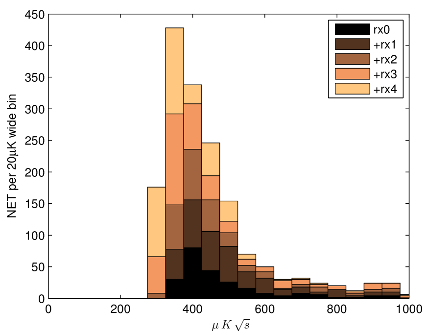
We have measured the devices’ performance on the sky during lengthy Bicep2 and Keck Array observation campaigns. The sensitivity of the experiment can be measured using the timestream noise between 0.1–1 Hz, after calibrating to the CMB. Bicep2 had a noise equivalent temperature (NET) of 16 . The larger detector complement of the Keck Array achieved 11.5 and 9 in 2012 and 2013, respectively, also at 150 GHz. Figure 21 shows the distribution of per-detector sensitivity for the Keck Array in 2013.
Another measure of instrument performance is the total map depth achieved, defined as the noise within a map pixel of a specific size. This is a function of instrumental sensitivity, scan strategy, and observing time. Over three seasons of observing, Bicep2 achieved an rms noise of (). (Bicep2 Collaboration II (2014), Bicep2 Collaboration I (2014)). Over two years, the five Keck Array 150 GHz cameras achieved (). Combining Bicep2 and Keck Array and averaging across the entire effective area 400 square degree field results in rms noise of .
9. Conclusions and future work
We have demonstrated our novel detectors’ performance through 18 camera-years of observations in the Bicep2/Keck Array program, including a detection reported in 2014 of degree-scale B-mode anisotropy (Bicep2 Collaboration I, 2014). This paper has described the design principles, challenges, fabrication techniques and our characterization/screening program that made these deployments possible. This program has continued through the recent, successful 2015 Spider flight and higher frequency upgrades to Keck Array.
We have also deployed Bicep3 in the current (2014-2015) Antarctic summer season, which has 1152 95 GHz detectors in a single camera. Once all the detectors are installed in the 2015-2016 season, this instrument will support 2560 95 GHz detectors. We package these detectors in individual modules that efficiently fill the focal plane and we illuminate the detectors’ antennas with non-uniform Gaussian tapered slot illuminations to reduce spillover onto the camera’s stop. These recent modifications will be the subject of a future paper.
Lastly, our detector technology allows for multi-color focal planes where different color channels are co-located on the focal plane. Most competing dual-band detector technologies use a single common aperture for all color channels and thus there is a reduction in per-detector efficiency due to aperture spillover (O’Brient et al., 2013). Planar antenna arrays allow each color to have a custom aperture, thus more efficiently using of both focal plane real estate and limited readout capacity. These are under active development for Bicep3 further upgrades to the Bicep/Keck Array program, and for future Spider flights.
References
- Battistelli et al. (2008) Battistelli, E., Amiri, M., Burger, B., et al. 2008, Journal of Low Temperature Physics, 151, 908
- Bicep2 Collaboration I (2014) Bicep2 Collaboration I. 2014, Phys. Rev. Lett., 112, 241101
- Bicep2 Collaboration II (2014) Bicep2 Collaboration II. 2014, The Astrophysical Journal, 792, 62
- Bicep2 Collaboration III (2015) Bicep2 Collaboration III. 2015, In prep.
- Bicep2 Collaboration IV (2014) Bicep2 Collaboration IV. 2014, In prep.
- Bodharamik et al. (1971) Bodharamik, P., Besser, L., & Newcomb, R. 1971, Circuit Theory, IEEE Transactions on, 18, 610
- Corp (2009a) Corp, C. S. T. 2009a, CST Microwave Suite User manual (CST-AG)
- Corp (2009b) Corp, S. 2009b, Sonnet User manual v. 12.52 (Sonnet)
- Das & Pozar (1987) Das, N., & Pozar, D. M. 1987, Microwave Theory and Techniques, IEEE Transactions on, 35, 326
- de Korte et al. (2003) de Korte, P. A. J., Beyer, J., Deiker, S., et al. 2003, Review of Scientific Instruments, 74, 3807
- Duband & Collaudin (1999) Duband, L., & Collaudin, B. 1999, Cryogenics, 39, 659
- Fabrega et al. (2009) Fabrega, L., Fernandez-Martinez, I., Gil, O., et al. 2009, Applied Superconductivity, IEEE Transactions on, 19, 460
- Fraisse et al. (2013) Fraisse, A. A., Ade, P. A. R., Amiri, M., et al. 2013, J. Cosmology Astrophys. , 4, 47
- Galbraith & Rebeiz (2008) Galbraith, C., & Rebeiz, G. 2008, Microwave Theory and Techniques, IEEE Transactions on, 56, 1675
- Gildemeister et al. (1999) Gildemeister, J. M., Lee, A. T., & Richards, P. L. 1999, Applied Physics Letters, 74, 868
- Gildemeister et al. (2001) —. 2001, Appl. Opt., 40, 6229
- Hammerstad & Jensen (1980) Hammerstad, E., & Jensen, O. 1980, in Microwave symposium Digest, 1980 IEEE MTT-S International, 407–409
- Irwin & Hilton (2005) Irwin, K., & Hilton, G. 2005, in Cryogenic Particle Detection (Heidlberg: Springer-Verlag), 63–149
- Kamionkowski et al. (1997) Kamionkowski, M., Kosowsky, A., & Stebbins, A. 1997, Physical Review Letters, 78, 2058
- Kaplinghat et al. (2003) Kaplinghat, M., Knox, L., & Song, Y.-S. 2003, Physical Review Letters, 91, 241301
- Kominami et al. (1985) Kominami, M., Pozar, D. M., & Schaubert, D. 1985, Antennas and Propagation, IEEE Transactions on, 33, 600
- Kuo et al. (2008) Kuo, C. L., Bock, J. J., Bonetti, J. A., et al. 2008, in Society of Photo-Optical Instrumentation Engineers (SPIE) Conference Series, Vol. 7020, Society of Photo-Optical Instrumentation Engineers (SPIE) Conference Series
- Martin & Puplett (1970) Martin, D., & Puplett, E. 1970, Infrared Physics, 10, 105
- Mather (1982) Mather, J. C. 1982, Appl. Opt., 21, 1125
- Myers et al. (2005) Myers, M. J., Holzapfel, W., Lee, A. T., et al. 2005, Applied Physics Letters, 86, 114103
- O’Brient et al. (2012) O’Brient, R., Ade, P. A. R., Ahmed, Z., et al. 2012, Proc. SPIE, 8452, 84521G
- O’Brient et al. (2013) O’Brient, R., Ade, P., Arnold, K., et al. 2013, Applied Physics Letters, 102, 063506
- Orlando et al. (2009) Orlando, A., Aikin, R. W., Amiri, M., et al. 2009, AIP Conference Proceedings, 1185, 471
- Stiehl et al. (2011) Stiehl, G., Cho, H.-M., Hilton, G., et al. 2011, Applied Superconductivity, IEEE Transactions on, 21, 298
- Takahashi et al. (2010) Takahashi, Y. D., Ade, P. A. R., Barkats, D., et al. 2010, Astrophys. J. , 711, 1141
- Turner et al. (2001) Turner, A. D., Bock, J. J., Beeman, J. W., et al. 2001, Appl. Opt., 40, 4921
- Williams et al. (2003) Williams, K., Gupta, K., & Wasilik, M. 2003, Microelectromechanical Systems, Journal of, 12, 761
- Zaldarriaga & Seljak (1997) Zaldarriaga, M., & Seljak, U. 1997, Phys. Rev. D , 55, 1830