Interplay of relativistic and nonrelativistic transport in atomically precise segmented graphene nanoribbons
Abstract
Graphene’s isolation launched explorations of fundamental relativistic physics originating from the planar honeycomb lattice arrangement of the carbon atoms, and of potential technological applications in nanoscale electronics. Bottom-up fabricated atomically-precise segmented graphene nanoribbons, SGNRs, open avenues for studies of electrical transport, coherence, and interference effects in metallic, semiconducting, and mixed GNRs, with different edge terminations. Conceptual and practical understanding of electric transport through SGNRs is gained through nonequilibrium Green’s function (NEGF) conductance calculations and a Dirac continuum model that absorbs the valence-to-conductance energy gaps as position-dependent masses, including topological-in-origin mass-barriers at the contacts between segments. The continuum model reproduces the NEGF results, including optical Dirac Fabry-Pérot (FP) equidistant oscillations for massless relativistic carriers in metallic armchair SGNRs, and an unequally-spaced FP pattern for mixed armchair-zigzag SGNRs where carriers transit from a relativistic (armchair) to a nonrelativistic (zigzag) regime. This provides a unifying framework for analysis of coherent transport phenomena and interpretation of forthcoming experiments in SGNRs.
Graphene, a single-atom-thin plane of graphite, has been the focus of intensive research endeavors since its isolation in 2004.geim04 The high degree of interest in this material originates from its outstanding electronic, mechanical, and physical properties that result from the planar arrangement of the carbon atoms in a honeycomb lattice. Indeed graphene is considered both as a vehicle for exploring fundamental relativistic physics, as well as a promising material for potential technological applications in nanoscale electronics and optics.razabook
However, the absence of an electronic energy gap between the valence and conduction bands of 2D graphene casts doubts on its use in nanoelectronic devices. Nevertheless, theoretical studies had predicted that narrow graphene nanoribbons (GNRs) can have a large band gap, comparable to silicon ( 1 eV), depending on the ribbon’s width and edge geometry (as well as possible doping at controlled positions). Pertinent to our work, we note that these predictions were made fuji96 ; cohe06 ; scus06 ; wang07 ; waka10 for GNRs that have atomically precise armchair edges with widths nm. Consequently, the most recent advent and growing availability of bottom-up fabricated atomically-precise narrow graphene nanoribbons, ruff10 ; huan12 ; derl13 ; nari14 ; sini14 including segmented ruff12 armchair graphene nanoribbons (SaGNRs), opens promising avenues for graphene nanoelectronics and for detailed explorations of coherent electrical transport in nanoribbon-based graphene wires, nanoconstrictions, and quantum-point contacts.
Here we report on the unique apects of transport through segmented GNRs obtained from tight-binding non-equilibrium Green’s function dattabook (TB-NEGF) calculations in conjunction with an analysis based on a one-dimensional (1D) relativistic Dirac model. This model is referred to by us as the Dirac-Fabry-Pérot (DFP) theory (see below for the choice of name). In particular, it is shown that the valence-to-conduction energy gap in armchair GNR (aGNR) segments, as well as the barriers at the interfaces between nanoribbon segments, can be incorporated in an effective position-dependent mass term in the Dirac hamiltonian; the transport solutions associated with this hamiltonian exhibit conductance patterns comparable to those obtained from the microscopic NEGF calculations. For zigzag graphene nanoribbon (zGNR) segments, the valence-to-conduction energy gap vanishes, and the mass term is consonant with excitations corresponding to massive nonrelativistic Schrödinger-type carriers.
As aforementioned, transport through narrow graphene channels particularly bottom-up fabricated and atomically-precise graphene nanoribbons ruff10 ; huan12 ; derl13 ; nari14 ; sini14 ; ruff12 is expected to offer ingress to unique behavior of Dirac electrons in graphene nanostructures. In particular, the wave nature of elementary particles (e.g., electrons and photons) is commonly manifested and demonstrated in transport processes. Because of an exceptionally high electron mobility and a long mean-free path, geim04 it has been anticipated that graphene devices hold the promise for the realization, measurement, and possible utilization of fundamental aspects of coherent and ballistic transport behavior, which to date have been observed, with varying degrees of success, mainly at semiconductor interfaces,hou89 ; ji03 quantum point contacts,vwee88 metallic wires,pasc95 and carbon nanotubes.lian01 Prominent among the effects that accompany coherence and ballistic transport are conductance quantization (in nanoconstrictions) in steps of , which have been found earlier for quantum ballistic transport in semiconductor point contactsvwee88 and metal nanowires.pasc95 However, quantization signatures were scarcely observed vwee11 in GNRs fabricated with top-down methods.
Another manifestation of coherent ballistic transport are interference phenomena, reflecting the wave nature of the transporting physical object, and associated most often with optical (electromagnetic waves, photons) systems or with analogies to such systems (that is, the behavior of massless particles, as in graphene sheets). Measurements of interference patterns are commonly made with the use of interferometers, most familiar among them the multi-pass optical Fabry-Pérot (OFP) interferometer,lipsbook where the superposition of all the outgoing light waves, bouncing in a cavity from bounding partially reflecting mirrors, yields an oscillatory intensity record (interference pattern) which depends on the light wavelength and the distance between the mirrors.
The quest for demonstration of the particle-wave duality of electrons through measurement of quantum interference phenomena associated with electron transport in solid-state devices requires materials and configurations having long mean-free paths. This requirement limited early experimental work in the late 1980s to semiconductor heterostructures,hou89 ; ji03 where conductance-quantization steps in gate-controlled two-dimensional constrictions have been observed. Subsequently interference patterns for nonrelativistic charge carriers in the form of conductance oscillations were observedlieb05 (and interpreted lieb05 ; land00 as Fabry-Pérot-type phenomena) in semiconductor nanowires. The advent of 2D forms of carbon allotropes has motivated the study of optical-like interference phenomena associated with relativistic massless electrons, as in the case of metallic carbon nanotubes lian01 and graphene 2D - junctions.rick13 (We note that the hallmark of the OFP is that the energy separation between successive maxima of the interference pattern varies as the inverse of the cavity length .)
For GNRs with segments of different widths, our investigations reveal diverse transport modes beyond the OFP case, with conductance quantization steps () found only for uniform GNRs. In particular, three distinct categories of Fabry-Pérot interference patterns are identified:
-
1.
FP-A: An optical FP pattern corresponding to massless graphene electrons exhibiting equal spacing between neighboring peaks. This pattern is associated with metallic armchair nanoribbon central segments. This category is subdivided further to FP-A1 and FP-A2 depending on whether a valence-to-conduction gap is absent (FP-A1, associated with metallic armchair leads), or present (FP-A2, corresponding to semiconducting armchair leads).
-
2.
FP-B: A massive relativistic FP pattern exhibiting a shift in the conduction onset due to the valence-to-conduction gap and unequal peak spacings. This pattern is associated with semiconducting armchair nanoribbon central segments, irrespective of whether the leads are metallic armchair, semiconducting armchair, or zigzag.
-
3.
FP-C: A massive non-relativistic FP pattern with peak spacings, but with a vanishing valence-to-conduction gap, being the length of the central segment. This pattern is the one expected for usual semiconductors described by the (nonrelativistic) Schrödinger equation, and it is associated with zigzag nanoribbon central segments, irrespective of whether zigzag or metallic armchair leads are used.
The faithful reproduction of these unique TB-NEGF conductance patterns by the DFP theory, including mixed armchair-zigzag configurations (where the carriers transit from a relativistic to a nonrelativistic regime), provides a unifying framework for analysis of coherent transport phenomena and for interpretation of experiments targeting fundamental understanding of transport in GNRs and the future development of graphene nanoelectronics.
Results
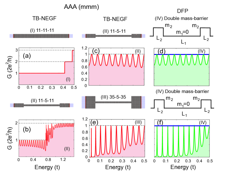
Segmented Armchair GNRs: All-metallic. Our findings for the case of all-metallicfuji96 ; waka10 segmented aGNRs (when the number of carbons specifying the width is , ) are presented in Fig. 1; this lattice configuration is denoted as AAA (mmm). A uniform metallic armchair GNR [see Fig. 1(I)] exhibits ballistic quantized-conductance steps [see Fig. 1(a)]. In contrast, conductance quantization is absent for a nonuniform 3-segment aGNR; see Figs. 1(b) 1(f). Instead of quantized steps, a finite number of oscillations appears, whose maxima (at the value of unity) maintain a constant energy separation. This behavior is indicative of optical-like Fabry-Pérot multiple reflections of the DW electron within the cavity defined by the two contacts (interfaces between the segments of different width). The patterns in Figs. 1(b) 1(f) correspond to the category FP-A1.
The dependence of the conductance on the width of the leads relative to that of the constriction is explored by comparing the two junctions (exhibiting sharp lead-to-constriction interfaces) depicted in Fig. 1(II) and Fig. 1(III). Examination of the TB-NEGF conductances for these two segmented aGNRs [Fig. 1(c) and Fig. 1(e)] reveals that a wider lead [Fig. 1(III)] is associated with a stronger confinement (sharp conductance spikes) compared to a narrower lead [Fig. 1(II)] (oscillations). In the DFP results [Fig. 1(d) and Fig. 1(f)], which reproduce the TB-NEGF results, this trend is accounted for by varying the length and height of the mass barriers, which generates either a weak coupling (closed quantum-dot-like conductance spikes) or a strong coupling (open quantum-dot-like Fabry-Pérot-type oscillations) to the leads.
Further insight can be gained by an analysis of the discrete energies associated with the humps of the conductance oscillations in Fig. 1(c) and the resonant spikes in Fig. 1(e). Indeed a simplified approximation for the electron confinement in the continuum model consists in considering the graphene electrons as being trapped within a 1D infinite-mass square well (IMSW) of length (the mass terms are infinite outside the interval and the coupling to the leads vanishes). The discrete spectrum of the electrons in this case is given fiol96 by
| (1) |
where the wave numbers are solutions of the transcendental equation
| (2) |
In the context of Fig. 1, (massless DW electrons), and one finds for the spectrum of the IMSW model:
| (3) |
with . Remarkably, the energies associated with the TB-NEGF oscillation humps and spikes in Figs. 1(c) and 1(e) [or Figs. 1(d) and 1(f) in the DFP model] follow very closely the above relation. Note the constant separation between successive energies,
| (4) |
which is twice the energy
| (5) |
of the lowest state.
As is well known, a constant energy separation of the intensity peaks, inversely proportional to the length of the resonating cavity [here , see Eqs. (4) and (5) above] is the hallmark of the optical Fabry-Pérot, reflecting the linear energy dispersion of the photon in optics or a massless DW electron in graphene structures. For our purpose, most revealing is the energy offset away form zero of the first conductance peak, which equals exactly one-half of the constant energy separation between the peaks. In onedimension, this is the hallmark of a massless fermion subject to an infinite- mass-barrier confinement, fiol96 and it provides ultimate support for our introduction of mass barriers at the interfaces of the segmented aGNR. Naturally, in the case of a semiconducting segment (see below), this equidistant behavior and -offset of the conductance peaks do not apply; this case is accounted for by the Dirac-Fabry-Pérot model presented in Methods, and it is more general than the optical Fabry-Pérot theory associated with a photonic cavity.lipsbook
In the nonrelativistic limit, i.e., when , one gets
| (6) |
which yields the well known relations and
| (7) |
For a massive relativistic electron, as is the case with the semiconducting aGNRs in this paper, one has to numerically solve Eq. (2) and then substitute the corresponding value of in Einstein’s energy relation given by Eq. (1).
It is worth mentioning here that the inoperativeness for one-dimensional cases, due to Klein tunneling, kats06 of the electrostatic potential [see horizontal blue lines at in Figs. 1(d) and 1(f)] was also noted earlier; see the curves for normal incidence (labeled ) in Fig. 2 of Ref. rodr12, .
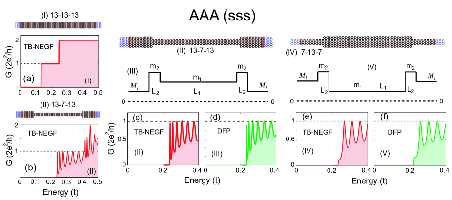
Segmented Armchair GNRs: All-semiconducting. Our results for a 3-segment all-semiconducting aGNR are portrayed in Fig. 2 [see schematic lattice diagrams in Figs. 2(I) and 2(II)]; this lattice configuration is denoted as AAA (sss). A uniform semiconducting armchair GNR [see Fig. 2(I)] exhibits ballistic quantized-conductance steps [see Fig. 2(a)]. In contrast, conductance quantization is absent for a nonuniform 3-segment () aGNR; see Figs. 2(b) 2(d). Here, instead of quantized steps, oscillations appear as in the case of the all-metallic junctions presented earlier in Fig. 1. However, the first oscillation appears now at an energy , which reflects the intrinsic gap of the semiconducting central segment belonging to the class II of aGNRs, specifiedwaka10 ; yann14 by a width , . That the leads are semiconducting does not have any major effect. This is due to the fact that , and as a result the energy gap of the central segment is larger than the energy gap of the semiconducting leads [see schematic in Fig. 2(III)].
The armchair GNR case with interchanged widths (i.e., instead of ) is portrayed in Figs. 2(e) 2(f). In this case the energy gap of the semiconducting leads (being the largest) determines the onset of the conductance oscillations. It is a testimonial of the consistency of our DFP method that it can reproduce [see Fig. 2(d) and Fig. 2(f)] both the and TB-NEGF conductances; this is achieved with very similar sets of parameters taking into consideration the central-segment-leads interchange. We note that the larger spacing between peaks (and also the smaller number of peaks) in the case is due to the smaller mass of the central segment ( instead of ).
From an inspection of Fig. 2, one can conclude that the physics associated with the all-semiconducting AAA junction is that of multiple reflections of a massive relativistic Dirac fermion bouncing back and forth from the edges of a particle box created by a double-mass barrier [see the schematic of the double-mass barrier in Fig. 2(III)]. In particular, to a good approximation the energies of the conductance oscillation peaks are given by the IMSW Eq. (2) with () or (). In this respect, the separation energy between successive peaks in Figs. 2(b), 2(c), 2(e), and 2(f) is not a constant, unlike the case of the all-metallic junction.
The patterns in Figs. 2(c) and 2(f) correspond to the category FP-B. This generalized oscillations cannot be accounted for by the optical Fabry-Pérot theory, but they are well reproduced by the generalized Dirac-Fabry-Pérot model introduced by us in the Methods.
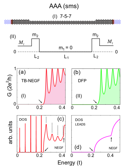
Segmented Armchair GNRs: semiconducting-metallic-semiconducting. Our results for a 3-segment () semiconducting-metallic-semiconducting aGNR are portrayed in Fig. 3 [see schematic lattice diagram in Fig. 3(I)]; this lattice configuration is denoted as AAA (sms). The first FP oscillation in the TB-NEGF conductance displayed in Fig. 3(a) appears at an energy , which reflects the intrinsic gap of the semiconducting leads (with ). The energy spacing between the peaks in Fig. 3(a) is constant in agreement with the metallic (massless DW electrons) character of the central segment with . The TB-NEGF pattern in Fig. 3(a) corresponds to the Fabry-Pérot category FP-A2. As seen from Fig. 3(b), our generalized Dirac-Fabry-Pérot theory is again capable of faithfully reproducing this behavior.
A deeper understanding of the AAA (sms) case can be gained via an inspection of the density of states (DOS) plotted in Fig. 3(c) for the total segmented aGNR (central segment plus leads) and in Fig. 3(d) for the the isolated leads. In Fig. 3(c), nine equidistant resonance lines are seen. Their energies are close to those resulting from the IMSW Eq. (3) (with , see the caption of Fig. 3) for a massless DW electron. Out of these nine resonances, the first five do not conduct [compare Figs. 3(a) and 3(c)] because their energies are lower than the minimum energy (i.e., ) of the incoming electrons in the leads [see the onset of the first band (marked by an arrow) in the DOS curve displayed in Fig. 3(d)].
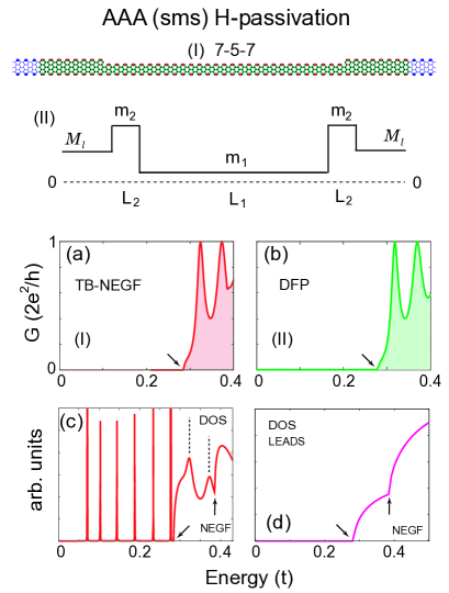
Segmented Armchair GNRs: Effects of hydrogen passivation. As shown in Refs. cohe06, ; wang07, , a detailed description of hygrogen passivation requires that the hopping parameters for the nearest-neighbor C-C bonds at the armchair edges be given by . Taking this modification into account, our results for a 3-segment semiconducting-metallic-semiconducting aGNR are portrayed in Fig. 4 [see schematic lattice diagram in Fig. 4(I)]; this lattice configuration is denoted as ”AAA (sms) H-passivation.” The first FP oscillation in the TB-NEGF conductance displayed in Fig. 4(a) appears at an energy , which reflects the intrinsic gap of the properly passivated semiconducting leads (with ). The energy spacing between the peaks in Fig. 4(a) is slightly away from being constant in agreement with the small mass acquired by the central segment with , due to taking . As seen from Fig. 4(b), our generalized Dirac-Fabry-Pérot theory is again capable of faithfully reproducing this behavior.
A deeper understanding of the AAA (sms)-H-passivation case can be gained via an inspection of the DOS plotted in Fig. 4(c) for the total segmented aGNR (central segment plus leads) and in Fig. 4(d) for the isolated leads. In Fig. 4(c), eight (almost, but not exacrly, equidistant) resonance lines are seen. Their energies are close to those resulting from the IMSW Eq. (2) (with and ; see the caption of Fig. 4) for a Dirac electron with a small mass. Out of these eight resonances, the first six do not conduct [compare Figs. 4(a) and 4(c)] because their energies are lower than the minimum energy (i.e., ) of the incoming electrons in the leads [see the onset of the first band (marked by an arrow) in the DOS curve displayed in Fig. 4(d)]. From the above we conclude that hydrogen passivation of the aGNR resulted in a small shift of the location of the states, and opening of a small gap for the central metallic narrower (with a width of ) segment, but did not modify the conductance record in any qualitative way. Moreover, the passivation effect can be faithfully captured by the Dirac FP model by a small readjustment of the model parameters.
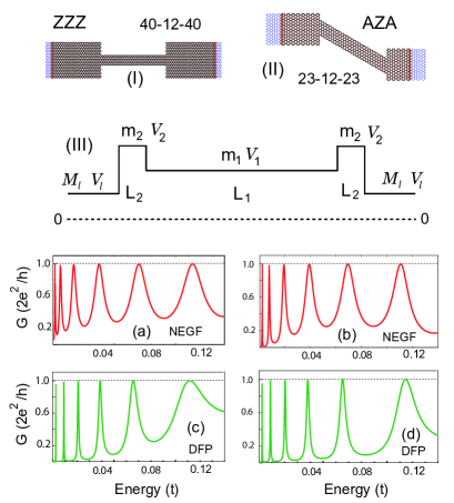
All-zigzag segmented GNRs. It is interesting to investigate the sensitivity of the interference features on the edge morphology. We show in this section that the relativistic transport treatment applied to segmented armchaie GNRs does not maintain for the case of a nanoribbon segment with zigzag edge terminations. In fact zigzag GNR (zGNR) segments exhibit properties akin to the well-known transport in usual semiconductors, i.e., their excitations are governed by the nonrelativistic Schrödinger equation.
Before discussing segmented GNRs with zigzag edge terminations, we remark that such GNRs with uniform width exhibit stepwise quantization of the conductance, similar to the case of a uniform metallic armchair-edge-terminated GNR [see Fig. 2(a)].
In Fig. 5(a), we display the conductance in a three-segment junction [see lattice schematic in Fig. 5(I)] when all three segments have zigzag edge terminations (denoted as ZZZ). The main finding is that the central segment behaves again as a resonant cavity that yields an oscillatory conductance pattern where the peak spacings are unequal [Fig. 5(a)]. This feature, which deviates from the optical Fabry-Pérot behavior, appeared also in the DFP patterns for a three-segment armchair junction whose central segment was semiconducting, albeit with a different dependence on [see Figs. 2 and Eq. (2)]. Moreover, from a set of systematic calculations (not shown) employing different lengths and widths, we found that the energy of the resonant levels in zGNR segments varies on the average as , where the integer counts the resonances and indicates the length of the central segment. However, a determining difference with the armchair GNR case in Fig. 2 is the vanishing of the valence-to-conductance gap in the zigzag case of Fig. 5(a). It is well known that the above features are associated with resonant transport of electronic excitations that obey the second-order nonrelativistic Schrödinger equation.
Naturally, one could formulate a continuum transport theory based on transfer matrices (see Methods) that use the 1D Schrödinger equation instead of the generalized Dirac Eq. (8). Such a Schrödinger-equation continuum approach, however, is unable to describe mixed armchair-zigzag interfaces (see below), where the electron transits between two extreme regimes, i.e., an ultrarelativistic (i.e., including the limit of vanishing carrier mass) Dirac regime (armchair segment) and a nonrelativistic Schrödinger regime (zigzag segment). We have thus been led to adopt the same Dirac-type transfer-matrix approach as with the armchair GNRs, but with nonvanishing potentials , with , where is the Heaviside step function. This amounts to shifts (in opposite senses) of the energy scales for particle and hole excitations, respectively, and it yields the desired vanishing value for the valence-to-conduction gap of a zigzag GNR.
The calculated DFP conductance that reproduces well the TB-NEGF result for the ZZZ junction [Fig. 5(a)] is displayed in Fig. 5(c); the parameters used in the DFP calculation are given in the caption of Fig. 5. We note that the carrier mass () in the central zigzag segment exhibits an energy dependence. This is similar to a well known effect (due to nonparabolicity in the dispersion) in the transport theory of usual semiconductors.melc93 We further note that the average mass associated with a zigzag segment is an order of magnitude larger than that found for semiconducting armchair segments of similar width (see captions in Fig. 2, and this yields energy levels close to the nonrelativistic limit [see Eq. (7)]. We note that FP pattern of the ZZZ junction belongs to the category FP-C.
Mixed armchair-zigzag-armchair segmented GNRs. Fig. 5 (right column) presents an example of a mixed armchair-zigzag-armchair (AZA) junction, where the central segment has again zigzag edge terminations [see lattice schematic in Fig. 5(II)]. The corresponding TB-NEGF conductance is displayed in Fig. 5(b). In spite of the different morphology of the edges between the leads (armchair) and the central segment (zigzag), the conductance profile of the AZA junction [Fig. 5(b)] is very similar to that of the ZZZ junction [Fig. 5(a)]. This means that the characteristics of the transport are determined mainly by the central segment, with the left and right leads, whether zigzag or armchair, acting as reservoirs supplying the impinging electrons.
The DFP result reproducing the TB-NEGF conductance is displayed in Fig. 5(d), and the parameters used are given in the caption. We stress that the mixed AZA junction represents a rather unusual physical regime, where an ultrarelativistic Dirac-Weyl massless electron (due to the metallic armchair GNRs in the leads) transits to a nonrelativistic massive Schrödinger one in the central segment. We note that FP pattern of the AZA junction belongs to the category FP-C.
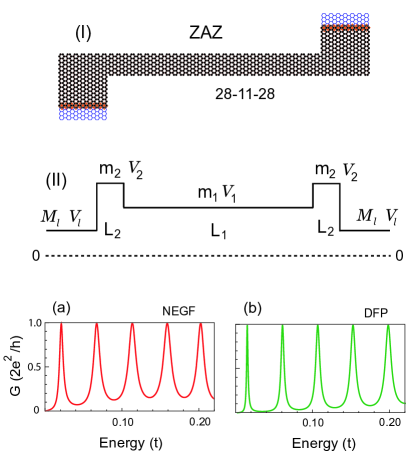
Mixed zigzag-armchair-zigzag segmented GNRs. Finally Fig. 6 presents an example of a mixed zigzag-armchair-zigzag (ZAZ) junction, where the central segment corresponds to a metallic armchair GNR [see lattice schematic in Fig. 6(I)]. The corresponding TB-NEGF conductance is displayed in Fig. 6(a). In spite of the different morphology of the edges between the leads (zigzag) and the central segment (armchair), the conductance profile of the ZAZ junction [Fig. 6(a)] is controlled by determined the central segment, with the left and right leads acting as reservoirs supplying the impinging electrons. Thus the conductance peaks are close to being equidistant, and the FP pattern belongs to the categoty FP-A1. The DFP result reproducing the TB-NEGF conductance is displayed in Fig. 6(b), and the parameters used are given in the caption.
In a reverse sense compared to the AZA junction above, the mixed ZAZ junction here represents also a rather unique physical regime, where a nonrelativistic massive Schrödinger electron (due to the zigzag GNRs in the leads) transits to an ultrarelativistic Dirac-Weyl massless one in the central segment. The decisive advances brought forward by our DFP 1D continuum theory can be clearly appreciated by its ability to describe the corresponding TB-NEGF results for these highly nontrivial ZAZ and AZA junctions [compare Figs. 6(a) and 6(b), as well as Figs. 5(b) and 5(d)]. Contimuum 2D formulations are unable to describe the important all-zigzag and mixed armchair/zigzag junctions described in this section, because they cannot distinguish between armchair and zigzag edges.
Discussion
To motivate the 1D Dirac formalism developed and utilized here, we note that customarily armchair or zigzag edge terminations in two-dimensional (2D) graphene nanoribbons are treated with the massless 2D Dirac equation with the use of the corresponding boundary conditions. brey06 In our study, however, narrow GNRs are treated with a 1D generalized Dirac equation. This approach is reminiscent of the 1D description of GNRs as described in Ref. zhen07, and also reviewed in Ref. waka10, , where the tight-binding 2D spectrum is projected onto the longitudinal wavenumber direction, . For the armchair case (see Eqs. 10 on Ref. zhen07, ), the low-energy range of the 1D spectrum can be well approximated by the Einstein energy relation with a non-zero mass term for the semiconducting case, and with a zero mass term for the metallic case which exhibits a massless linear dependence (photon-like dispersion) of the energy on the momentum.
As a function of , the zigzag GNRs exhibit a partially flat band due to the localized (in the transverse direction) edge state. The flat part is centered around (alternatively taken as in Ref. brey06, ), where , and it expands towards the graphene Dirac points located at (alternatively, ) and (alternatively ) as the width of the ribbon increases (see Fig. 7 in Ref. waka10, ). After reaching the ends of the flat part, the energy band opens two branches with non-zero energies; these branches do not have a linear dependence on . Although this can be termed also as a “gapless” spectrum (like the metallic armchair case), the two differ in their dispersion relation – that is the energy of the former (zigzag) is approximately independent of the momentum for a broad range of the momentum (see examples for various widths of zigzag GNRs in Fig. 4 of Ref. waka10, ), whereas the latter (armchair) shows a linear energy-momentum relationship (see Fig. 3 in Ref. waka10, ).
As the width of the GNRs get smaller (narrow zigzag nanoribbons), the range of the aforementioned flat part decreases, and in the limit of a single row of benzene rings (the narrow-most zigzag GNR, referred to as polyacene) the dispersion curve transforms kive83 into two (electron-hole) parabolas touching at . The spectrum of polyacene is gapless, but due to the nonrelativistic parabolic dispersion, a mass, , is associated kive83 with the second derivative according to the nonrelativistic relation . The case of narrow zigzag GNRs that we study here is closer to the nonrelativistic polyacene than to the relativistic massless graphene (i.e., the limit of a zigzag ribbon of infinite width). Incidentally, we mention that the polyacene parabolic-band limit is not obtained onip08 through a treatment employing the massless 2D Dirac equation with boundary conditions.
We comment here that physical circumstances where a change in some system configuration can result in a change in the nature of the dispersion relation (e.g from linear to quadratic), are not that rare. Another example is found when comparing the gapless, but linear in momentum, dispersion of the energy of particles (massless relativistic) in a monolayer 2D graphene sheet with the gapless, but parabolic, dispersion (massive non-relativistic particles) in bilayer graphene.mcca13
Furthermore, our NEGF conductance calculations for segmented zigzag GNRs exhibited Fabry-Pérot oscillatory patterns, with the spacing between peaks behaving as (where is the length of the GNR segment). This differs from the (photon-like) FP pattern found for the metallic case of armchair GNRs where the spacing between peaks in the oscillatory conductance varies as (characteristic of massless particles with linear energy-momentum dispersion, e.g. photons), which were studied lipsbook by Fabry and Pérot. This directly suggests that the zigzag GNRs can be described by a nonrelativistic limit of the Dirac equation with a sufficiently large mass (i.e. by the Schrödinger equation).
Focusing on the intrinsic properties of the graphene lattice, originating from the topology of the honeycomb network, and using a NEGF approach, we have studied here the transport properties of atomically precise segmented armchair and zigzag graphene nanoribbons, with segments of different widths. Mixed armchair-zigzag junctions (with segments of different widths) have also been discussed.
The electronic conductance is found to exhibit Fabry-Pérot oscillations, or resonant tunneling, associated with partial confinement and formation of a quantum box (resonant cavity) in the junction. The Fabry-Pérot oscillations occur for junctions that are strongly coupled to the leads (open system), whereas the resonant-tunneling spikes appear for weak lead-junction coupling (closed system). In particular, with regard to the FP interference patterns, three distinct categories were identified (see the Introduction), with only one of them having the characteristics of the optical lipsbook FP pattern corresponding to massless graphene electrons exhibiting equal spacings between neighboring peaks.
Perfect quantized-conductance flat steps were found only for uniform GNRs. In the absence of extraneous factors, like disorder, in our theoretical model, the deviations from the perfect quantized-conductance steps were unexpected. However, this aforementioned behavior obtained through TB-NEGF calculations is well accounted for by a 1D contimuum fermionic Dirac-Fabry-Pérot interference theory (see Methods). This approach employs an effective position-dependent mass term in the Dirac Hamiltonian to absorb the finite-width (valence-to-conduction) gap in armchair nanoribbon segments, as well as the barriers at the interfaces between nanoribbon segments forming a junction. For zigzag nanoribbon segments the mass term in the Dirac equation reflects the nonrelativistic Schrödinger-type behavior of the excitations. We emphasize that the mass in zigzag-terminated GNR segments is much larger than the mass in semiconducting armchair-terminated GNR segments. Furthermore in the zigzag GNR segments (which are always characterized by a vanishing valence-to-conduction energy gap), the mass corresponds simply to the carrier mass. In the armchair GNR segments, the carrier mass endows (in addition) the segment with a valence-to-conduction energy gap, according to Einstein’s relativistic energy relation [see Eq. (1)].
We observe here that the Dirac Fabry-Pérot masses that we find to yield agreement with the TB conductance spectra agree well with those obtained through Density Functional Theory (DFT) calculations cohe06 where the energy gap for armchair GNRs versus width has been determined. For example, for and , Eq. (1) in Ref. cohe06, yields and , respectively. These DFT values agree well with the DFP values of (central segment) and (leads) given in the caption of Fig. 4, where the H-passivation effect according to the DFT was incorporated in the TB description.
The above findings point to a most fundamental underlying physics, namely that the topology of disruptions of the regular honeycomb lattice (e.g., variable width segments, corners, edges) generate a scalar-potential field (position-dependent mass, identified also as a Higgs-type field yann14 ; roma13 ), which when integrated into a generalized Dirac equation for the electrons provides a unifying framework for the analysis of transport processes through graphene constrictions and segmented junctions.
With growing activities and further improvements in the areas of bottom-up fabrication and manipulation
of atomically precise ruff10 ; huan12 ; derl13 ; nari14 ; sini14
graphene nanostructures and the anticipated measurement
of conductance through them, the above findings could serve as impetus and implements
aiding the design and interpretation of future experiments.
Methods
Dirac-Fabry-Pérot model.
The energy of a relativistic fermion (with one-dimensional momentum ) is given by the Einstein relation
, where is the rest mass and is the
Fermi velocity of graphene. (In a uniform armchair graphene nanoribbon, the mass parameter is related to the
particle-hole energy gap, , as .) Following the relativisitic
quantum-field Lagrangian formalism, the mass is replaced by a position-dependent scalar
Higgs field , to which the relativistic fermionic field couples
through the Yukawa Lagrangian roma13
( being a Pauli matrix). For (constant) , and
the massive fermion Dirac theory is recovered. The Dirac equation is generalized as (here we do not
consider applied electric or magnetic fields)
| (8) |
In one dimension, the fermion field is a two-component spinor ; and stand, respectively, for the upper and lower component and and can be any two of the three Pauli matrices. Note that the Higgs field enters in the last term of Eq. (8). in the first term is the usual electrostatic potential, which is inoperative due to the Klein phenomenon kats06 ; rodr12 and thus is set to zero for the case of the armchair nanoribbons (where the excitations are relativistic). The generalized Dirac Eq. (8) is used in the construction of the transfer matrices of the Dirac-Fabry-Pérot model described below.
The building block of the DFP model is a 22 wave-function matrix formed by the components of two independent spinor solutions (at a point ) of the onedimensional, first-order generalized Dirac equation [see Eq. (3) in the main paper]. plays mcke87 the role of the Wronskian matrix used in the second-order nonrelativistic Kronig-Penney model. Following Ref. mcke87, and generalizing to regions, we use the simple form of in the Dirac representation (, ), namely
| (9) |
where
| (10) |
The transfer matrix for a given region (extending between two matching points and specifying the potential steps ) is the product ; this latter matrix depends only on the width of the region, and not separately on or .
The transfer matrix corresponding to a series of regions can be formed roma13 as the product
| (11) |
where is the width of the th region [with ]. The transfer matrix associated with the transmission of a free fermion of mass (incoming from the right) through the multiple mass barriers is the product
| (12) |
with , ; for armchair leads , while for zigzag leads . Naturally, in the case of metallic armchair leads, , since .
Then the transmission coefficient is
| (13) |
while the reflection coefficient is given by
| (14) |
At zero temperature, the conductance is given by ;
is the transmission coefficient in Eq. (13).
TB-NEGF formalism. To describe the properties of graphene nanostructures in the tight-binding approximation, we use the hamiltonian
| (15) |
with indicating summation over the nearest-neighbor sites . eV is the hopping parameter of two-dimensional graphene.
To calculate the TB-NEGF transmission coefficients, the Hamiltonian (15) is employed in conjunction with the well known transport formalism which is based on the nonequilibrium Green’s functions. dattabook
According to the Landauer theory, the linear conductance is , where the transmission coefficient is calculated as . The Green’s function is given by
| (16) |
with being the Hamiltonian of the isolated device (junction without the leads). The self-energies are given by , where the hopping matrices describe the left (right) device-to-lead coupling, and is the Hamiltonian of the semi-infinite left (right) lead. The broadening matrices are given by .
References
- (1) Novoselov, K.S. et al. Electric field effect in atomically thin carbon films. Science 306, 666 (2004).
- (2) Raza, H., Editor, Graphene Nanoelectronics: Metrology, Synthesis, Properties and Applications, (Springer, New York, 2012).
- (3) Nakada, K., Fujita, M., Dresselhaus, G. & Dresselhaus, M.S. Edge state in graphene ribbons: Nanometer size effect and edge shape dependence. Phys. Rev. B 54, 17954 (1996).
- (4) Son, Y.W., Cohen, M.L. & Louie, S.G. Energy Gaps in graphene nanoribbons. Phys. Rev. Lett. 97, 216803 (2006).
- (5) Wang, Z.F. et al. Tuning the electronic structure of graphene nanoribbons through chemical edge modification: A theoretical study. Phys. Rev. B 75, 113406 (2007).
- (6) Barone, V., Hod, O., & Scuseria, G.E. Electronic structure and stability of semiconducting graphene nanoribbons. Nano Lett. 6, 2748 (2006).
- (7) Wakabayashi, K., Sasaki, K., Nakanishi, T. & Enoki, T. Electronic states of graphene nanoribbons and analytical solutions. Sci. Technol. Adv. Mater. 11, 054504 (2010), and references therein.
- (8) Cai, J.M. et al. Atomically precise bottom-up fabrication of graphene nanoribbons. Nature 466, 470 (2010).
- (9) Huang, H. Spatially resolved electronic etructures of etomically precise armchair graphene nanoribbons. Sci. Rep. 2, 983 (2012).
- (10) Van der Lit, J. et al. Suppression of electron-vibron coupling in graphene nanoribbons contacted via a single atom. Nat. Commun. 4, 2023 (2013).
- (11) Narita, A. et al. Synthesis of structurally well-defined and liquid-phase-processable graphene nanoribbons. Nat. Chem. 6, 126 (2014).
- (12) Vo, T.H. et al. Large-scale solution synthesis of narrow graphene nanoribbons. Nat. Commun. 5, 3189 (2014).
- (13) Blankenburg, S. et al. Intraribbon heterojunction formation in ultranarrow graphene nanoribbons. ACS Nano 6, 2020 (2012).
- (14) Datta, S. Quantum Transport: Atom to Transistor, (Cambridge University Press, Cambridge, 2005).
- (15) van Houten, H., Beenakker, C.W.J., Williamson, J.G., Broekaart, M.E.I. & van Loosdrecht, P.H.M. Coherent electron focusing with quantum point contacts in a two-dimensional electron gas. Phys. Rev. B 39, 8556 (1989).
- (16) Ji, Y. et al. An electronic Mach-Zehnder interferometer. Nature 422, 415 (2003).
- (17) vanWees, B.J. et al. Quantized conductance of point contacts in a two-dimensional electron gas. Phys. Rev. Lett. 60, 848 (1988).
- (18) Pascual, J.I. et al. Properties of metallic nanowires: from conductance quantization to localization. Science 267, 1793 (1995).
- (19) Liang, W. et al. Fabry-Pérot interference in a nanotube electron waveguide. Nature 411, 665 (2001).
- (20) Tombros, N. et al. Quantized conductance of a suspended graphene nanoconstriction. Nat. Phys. 7, 697 (2011).
- (21) Lipson, S.G., Lipson, H. & Tannhauser, D.S. Optical Physics (Cambridge Univ. Press, London, 1995, 3rd ed.) p. 248.
- (22) Lu, W., Xiang, J., Timko, B.P., Wu, Y. & Lieber, C.M. One-dimensional hole gas in germanium/silicon nanowire heterostructures. Proc. Nat. Acad. Sci. 102, 10046 (2005).
- (23) Landman, U., Barnett, R.N., Scherbakov, A.G. & Avouris, Ph. Metal-semiconductor nanocontacts: Silicon nanowires. Phys. Rev. Lett. 85, 1958 (2000).
- (24) Rickhaus, P. et al. Ballistic interferences in suspended graphene. Nat. Commun. 4, 2342 (2013).
- (25) Alberto, P., Fiolhais, C. & Gil, V.M.S. Relativistic particle in a box. Eur. J. Phys. 17, 19 (1996).
- (26) Katsnelson, M.I., Novoselov, K.S. & Geim, A.K. Chiral tunnelling and the Klein paradox in graphene. Nature Phys. 2, 620 (2006).
- (27) Rodriguez-Vargas, I. et al. A comparative study of Klein and non-Klein tunneling structures. J. App. Phys. 112, 073711 (2012).
- (28) Yannouleas, C., Romanovsky, I. & U. Landman, U. Beyond the constant-mass Dirac physics: Solitons, charge fractionization, and the emergence of topological insulators in graphene rings. Phys. Rev. B 89, 035432 (2014).
- (29) López-Villanueva, J.A., Melchor, I., Cartujo, P. & Carceller, J.E. Modified Schrödinger-equation including nonparabolicity for the study of a two-dimensional electron gas. Phys. Rev. B 48, 1626 (1993).
- (30) Brey, L. & Fertig, H.A. Electronic states of graphene nanoribbons studied with the Dirac equation. Phys. Rev. B 73, 235411 (2006).
- (31) Zheng, H. et al. Analytical study of electronic structure in armchair graphene nanoribbons. Phys. Rev. B 75, 165414 (2007).
- (32) Kivelson, S. & Chapman, O.L. Polyacene and a new class of quasi-one-dimensional conductors. Phys. Rev. 28, 7236 (1983).
- (33) Onipko, A. Spectrum of pi electrons in graphene as an alternant macromolecule. Phys. Rev. B, 78, 245412 (2008)).
- (34) McCann, A. & Koshino, M. The electronic properties of bilayer graphene. Rep. Prog. Phys. 76, 056503 (2013).
- (35) Romanovsky, I., Yannouleas, C. & Landman, U. Topological effects and particle physics analogies beyond the massless Dirac-Weyl fermion in graphene nanorings. Phys. Rev. B 87, 165431 (2013).
- (36) McKellar, B.H.J. & Stephenson, Jr., G.J. Relativistic quarks in one-dimensional periodic structures. Phys. Rev. C 35, 2262 (1987).
Acknowledgements:
This work was supported by a grant from the Office of Basic Energy Sciences of
the US Department of Energy under Contract No. FG05-86ER45234. Computations were made at the GATECH
Center for Computational Materials Science.
Author Contributions: I.R. & C.Y. performed the computations. C.Y., I.R. & U.L. analyzed the
results. C.Y. & U.L. wrote the manuscript.
Competing financial interests: The authors declare no competing financial interests.
Correspondence should be addressed to C.Y.: (Constantine.Yannouleas@physics.gatech.edu).