Superpoissonian shot noise in organic magnetic tunnel junctions
Abstract
Organic molecules have recently revolutionized ways to create new spintronic devices. Despite intense studies, the statistics of tunneling electrons through organic barriers remains unclear. Here we investigate conductance and shot noise in magnetic tunnel junctions with PTCDA barriers a few nm thick. For junctions in the electron tunneling regime, with magnetoresistance ratios between 10 and 40%, we observe superpoissonian shot noise. The Fano factor exceeds in 1.5-2 times the maximum values reported for magnetic tunnel junctions with inorganic barriers, indicating spin dependent bunching in tunneling. We explain our main findings in terms of a model which includes tunneling through a two level (or multilevel) system, originated from interfacial bonds of the PTCDA molecules. Our results suggest that interfaces play an important role in the control of shot noise when electrons tunnel through organic barriers.
pacs:
72.25.Mk; 72.70.+m; 78.47.-pOrganic elements in electronic devices have some advantages over inorganic ones, like the ability to chemically adjust their electronic properties, their mechanical flexibility, and the capability to form self-assembled layers. Exploring the unique properties of the organic world to improve and create new functionalities in spin related optics, electronics and memory elements has been attracting considerable attention in the past decade Dediu et al. (2002); Xiong et al. (2004); Rocha et al. (2005); Santos et al. (2007); Sanvito (2011); Jiang et al. (2011); Vincent et al. (2012). Organic spintronics may lead to unique devices, for instance, organic light emitting diodes (OLEDs) based on magnetically controlled luminescence Nguyen et al. (2012). A key limiting factor for the operation of these and related devices is their signal to noise ratio. Thus, the investigation of noise sources in organic tunnel junctions and spin valves is of fundamental and technological interest, as the noise ultimately determines their practical applications.
Low frequency noise, and shot noise (SN) measurements have been systematically used to characterize the electronic transport mechanisms in inorganic spintronics Nowak et al. (1998); Guerrero et al. (2006, 2007); Scola et al. (2007); Almeida et al. (2008); Sekiguchi et al. (2010); Arakawa et al. (2011); Tanaka et al. (2014). On the other hand, noise in organic-based devices, which could have and shot noise contributions, remains poorly understood. For example, noise measurements have been used to determine device quality Clément et al. (2007), or transport features in graphene-based devices (including one or several layers) Balandin (2013). In another study, the noise and DC leakage measurements were used as a diagnostic tool for OLED reliability in a production line Rocha et al. (2013). Current noise measurements have been also used to identify individually contacted organic molecules Tsutsui (2010); Schaffert et al. (2012).
Earlier noise measurements in organic spintronic devices were carried out at large applied voltages, where the noise is dominant. Therefore, they were not able to unveil the role of shot noise, the most fundamental noise source in nanodevices. Apart from being important from the point of view of applications, precise knowledge of SN can provide a valuable information on electron correlations near the interfaces with organic barriers, especially in the regime of direct tunneling. In fact, the role of interfaces remains one of the central issues in organic spintronics Keevers et al. (2013).
Here, we analyze the tunneling statistics in organic magnetic tunnel junctions (O-MTJs) by measuring shot noise, which is known to be an excellent tool to investigate the correlations and other details of electron tunneling, well beyond the capabilities of transport measurements Blanter and B ttiker (2000); Bułka et al. (1999); Tserkovnyak and Brataas (2001); López and Sánchez (2003); Thielmann et al. (2003); Cottet et al. (2004); Belzig (2005); Souza et al. (2008); Chudnovskiy et al. (2008); Yamauchi et al. (2011a); Schneider et al. (2012). Being a consequence of the discrete nature of charge carriers, SN is the only contribution to the noise which survives down to low temperatures. The normalized shot noise (or Fano factor ) indicates Blanter and B ttiker (2000) whether the tunneling is uncorrelated (poissonian, ), anti-bunched (sub-poissonian, typically due to negative correlations, ) or bunched (super-poissonian, typically due to positive correlations, ).
We have investigated the conductance and shot noise of O-MTJs with PTCDA molecular barriers in the direct tunneling regime Li et al. (2011). In contrast to MTJs with inorganic barriers Guerrero et al. (2006, 2007), tunneling through molecular barriers shows super-poissonian shot noise which additionally depends on the relative alignment of the electrodes’ magnetization. Our observations are accounted for qualitatively within a model based on spin dependent electron tunneling through an interacting two-level (or multi-level) system.
The layer sequence in the PTCDA organic spin valves studied in this letter is: NiFe(25nm)/CoFe(15nm)/AlxO(0.6nm)/PTCDA(1.2-5nm)/AlxO(0.6nm)/CoFe(30nm). The structure was deposited onto a glass substrate, and the junctions were prepared in a high-vacuum environment with a base pressure lower than mbar. The metallic layers were deposited by sputtering with an Ar working pressure of mbar. The PTCDA layers were grown by thermal evaporation at mbar, with a deposition rate of 0.1 nm/s. Thin AlOx layers were grown between the PTCDA layer and both ferromagnetic layers by partially oxidizing Al in oxygen plasma for 5 s. Figure 1(a) shows a sketch of the investigated O-MTJs.
The voltage noise was measured using a cross-correlation technique, described elsewhereGuerrero et al. (2006, 2007). The correct calibration of our setup has been confirmed by independent studies Sekiguchi et al. (2010); Arakawa et al. (2011). The current noise power in the absence of correlations is Poissonian (full shot noise) and is given by , where is the average current and the electron charge. The voltage full SN is then , with being the dynamic resistance obtained from the corresponding curves. We have obtained the experimental SN, , by fitting a Gaussian peak to the histogram of the part of the spectra independent of frequency (see the Supplemental Material sup ). The Fano factor is then calculated as .
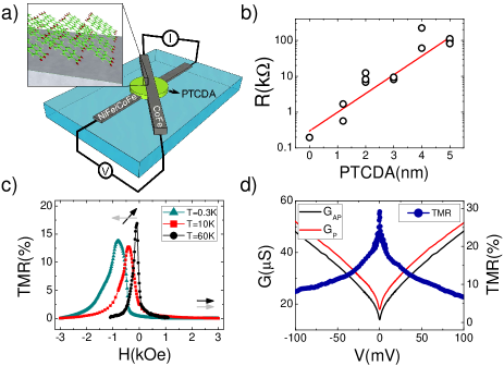
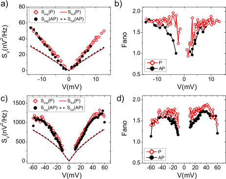
Figure 1(b) shows that the resistance of the junctions increases exponentially with the thickness of the PTCDA barrier. This indicates that the insulating PTCDA layer acts as a barrier in single step tunneling regime Schoonus et al. (2009). Figure 1(c) shows the tunneling magnetoresistance (TMR) for three different temperatures in a 2nm PTCDA O-MTJ, where the parallel (P) and antiparallel (AP) magnetic alignment of the electrodes are indicated by arrows. The TMR decreases when the bias reaches 100 mV (see Fig. 1(d)). Figure 1(d) also presents the differential conductance in the P and AP states as a function of the bias voltage at T=0.3K for a 4nm PTCDA O-MTJ. We found that the magnetic tunnel junctions with PTCDA barriers were more robust than conventional inorganic MTJs, and typically did not experience dielectrical breakdown as readily. Out of 14 samples studied, only 3 have degraded during multiple bias sweeps up to 500mV.
The experimental SN and at for the 2 nm PTCDA junction from Fig. 1(c) are shown in Fig. 2(a) for the P and AP states. Fig. 2(b) shows the dependence of the Fano factor with the bias for another samples with a 5 nm thick PTCDA barrier. As can be seen, the factor ranges from at low voltages to at higher voltages. All the O-MTJ samples measured displayed a qualitatively similar variation of the Fano factor with the bias voltage. The shot noise could be obtained for voltages up to a few tens of mV only. The maximum voltage for which the shot noise is measured corresponds to the energy at which the noise becomes dominant and obscures the frequency independent part of the noise spectrum. Even though the spectra could be obtained up to 100 kHz, filtering due to the capacitance of the samples (dependent on the PTCDA thickness) allowed shot noise measurements only between 1-10 kHz. The appearance of noise restricted SN measurements in all the studied samples, especially in the AP state.
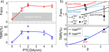
Figure 3(a) presents the average saturation value of the Fano factor in the P state for the samples which presented the frequency-independent spectra. Figure 3(a) also shows the variation of TMR with the PTCDA thickness. Control junctions, with only a 1.2nm AlOx layer, show TMR below 1%, and a metallic-like electron transport (see sup ). This points to diffusive electron transport, for which the theoryBlanter and B ttiker (2000) predicts the Fano factor equal to 1/3. Thus, control measurements prove that the super-poissonian SN is due to the PTCDA barriers. Our O-MTJs with PTCDA thicknesses between 1.2 and 5 nm show relatively high TMR and super-poissonian tunneling statistics with the Fano factor approaching 2, indicative of co-tunneling or tunneling with bunching. Eight O-MTJs of different barrier thicknesses, from four sample sets, have shown qualitatively similar SN values (Fig. 3(a)).
A number of electron tunneling mechanisms (Kondo effectYamauchi et al. (2011b), co-tunneling Onac et al. (2006); Okazaki et al. (2013), and others Lambert et al. (2007); Kießlich et al. (2007)) are capable of producing super-poissonian SN. However, they are mostly relevant for small quantum dots. The observed SN has been accounted for in terms of the approach developed by Belzig Belzig (2005), extended to spin dependent transport. The corresponding model is based on tunneling through a two-level system (or multi-level system in a more general case), with remarkably different tunneling rates through the two levels. Moreover, these tunneling rates are also spin dependent. The statistics of the transport process is described as a sum of independent Poissonian processes transferring bunches of electrons of different size. This arises from the difference in tunnel rates between the two levels and leads to an enhanced noise. Details of the model and description will be presented elsewhere. In Fig. 3(b) we show the TMR and Fano factor in the P and AP states as a function of the parameter , which describes the spin asymmetry in tunneling rates. The solid and dashed lines are the theoretical results, while the points correspond to the experimental data. Note that for each sample the TMR and Fano factors have been fitted with the same parameter , which justifies the validity of our approach.
Physically, the two or more levels with different couplings, which are responsible for the observed superpoissonian shot noise, can have their origin in localized states arising from interfacial bonds between the PTCDA molecules and the AlOx buffer layers. The following arguments suggest that the localized states in the model have an interfacial nature: (i) the exponential dependence of the tunneling resistance on PTCDA thickness (Fig. 1(b)) including the metallic character of the conductance when only the AlOx buffer layer is present (see sup ); (ii) a lateral size of the junctions larger than a micron, for which the influence of Coulomb blockade is minimized. The physical origin of the interfacial states could be a charge neutrality level Vázquez et al. (2004), or gap states Yogev et al. (2013), which appear due to the alignment of the energy levels at metal/organic interfaces Braun et al. (2009). The bias dependence of the interfacial density of states could explain the suppression of the Fano factor at large voltages (Fig. 2(b)).
In conclusion, super-poissonian statistics in tunneling events through the PTCDA molecular barriers have been unveiled by shot noise measurements. A superpoissonian shot noise has been found, which is likely due to localized states originated from interfacial bonds of the PTCDA molecules. For a technological application, the shot noise could be reduced or controlled, for instance, by the growth of double-barrierCascales et al. (2012) O-MTJs. Challenges for further work include extending the bias range where the shot noise could be investigated and comparing the role of the organic layers in the superpoissonian SN by the study of O-MTJs with different organic layers.
The authors acknowledge support by the Spanish MINECO (MAT2012-32743), UAM-SANTANDER, Comunidad de Madrid (P2013/MIT2850) and NSC 102-2120-M-002-005 (Taiwan) grants. This work is also partly supported by the National Center of Research and Development in Poland in the frame of the EU project Era.Net.Rus “SpinBarrier”.
References
- Dediu et al. (2002) V. Dediu, M. Murgia, F. Matacotta, C. Taliani, and S. Barbanera, Solid State Communications 122, 181 (2002), ISSN 0038-1098.
- Xiong et al. (2004) Z. H. Xiong, D. Wu, Z. Valy Vardeny, and J. Shi, Nature 427 (2004).
- Rocha et al. (2005) A. R. Rocha, V. Garcia-Suarez, S. W. Bailey, C. J. Lambert, J. Ferrer, and S. Sanvito, Nature Materials 4, 335 (2005).
- Santos et al. (2007) T. S. Santos, J. S. Lee, P. Migdal, I. C. Lekshmi, B. Satpati, and J. S. Moodera, Phys. Rev. Lett. 98, 016601 (2007).
- Sanvito (2011) S. Sanvito, Chemical Society Reviews 40 (2011).
- Jiang et al. (2011) J. S. Jiang, J. E. Pearson, and S. D. Bader, Phys. Rev. Lett. 106, 156807 (2011).
- Vincent et al. (2012) R. Vincent, S. Klyatskaya, M. Ruben, W. Wernsdorfer, and F. Balestro, Nature 488 (2012).
- Nguyen et al. (2012) T. D. Nguyen, E. Ehrenfreund, and Z. V. Vardeny, Science 337, 204 (2012).
- Nowak et al. (1998) E. R. Nowak, R. D. Merithew, M. B. Weissman, I. Bloom, and S. S. P. Parkin, Journal of Applied Physics 84 (1998).
- Guerrero et al. (2006) R. Guerrero, F. G. Aliev, Y. Tserkovnyak, T. S. Santos, and J. S. Moodera, Phys. Rev. Lett. 97, 266602 (2006).
- Guerrero et al. (2007) R. Guerrero, D. Herranz, F. G. Aliev, F. Greullet, C. Tiusan, M. Hehn, and F. Montaigne, Applied Physics Letters 91, 132504 (2007).
- Scola et al. (2007) J. Scola, H. Polovy, C. Fermon, M. Pannetier-Lecoeur, G. Feng, K. Fahy, and J. M. D. Coey, Applied Physics Letters 90, 252501 (2007).
- Almeida et al. (2008) J. M. Almeida, P. Wisniowski, and P. Freitas, Magnetics, IEEE Transactions on 44, 2569 (2008), ISSN 0018-9464.
- Sekiguchi et al. (2010) K. Sekiguchi, T. Arakawa, Y. Yamauchi, K. Chida, M. Yamada, H. Takahashi, D. Chiba, K. Kobayashi, and T. Ono, Applied Physics Letters 96, 252504 (2010).
- Arakawa et al. (2011) T. Arakawa, K. Sekiguchi, S. Nakamura, K. Chida, Y. Nishihara, D. Chiba, K. Kobayashi, A. Fukushima, S. Yuasa, and T. Ono, Applied Physics Letters 98, 202103 (2011).
- Tanaka et al. (2014) T. Tanaka, T. Arakawa, M. Maeda, K. Kobayashi, Y. Nishihara, T. Ono, T. Nozaki, A. Fukushima, and S. Yuasa, Applied Physics Letters 105, 042405 (2014).
- Clément et al. (2007) N. Clément, S. Pleutin, O. Seitz, S. Lenfant, and D. Vuillaume, Phys. Rev. B 76, 205407 (2007).
- Balandin (2013) A. A. Balandin, Nature Nanotechnology 8 (2013).
- Rocha et al. (2013) P. Rocha, H. Gomes, L. Vandamme, D. De Leeuw, S. Meskers, and P. van de Weijer, in Noise and Fluctuations (ICNF), 2013 22nd International Conference on (2013), pp. 1–4.
- Tsutsui (2010) M. K. T. Tsutsui, Makusu; Taniguchi, Nat Commun 1 (2010).
- Schaffert et al. (2012) J. Schaffert, M. Cottin, A. Sonntag, H. Karacuban, C. Bobisch, N. Lorente, J.-P. Gauyacq, and R. Muller, Nature Materials 12 (2012).
- Keevers et al. (2013) T. Keevers, A. Danos, T. Schmidt, and D. McCamey, Nat. Nanotech. 8, 886 (2013).
- Blanter and B ttiker (2000) Y. Blanter and M. B ttiker, Physics Reports 336 (2000).
- Bułka et al. (1999) B. R. Bułka, J. Martinek, G. Michałek, and J. Barnaś, Phys. Rev. B 60, 12246 (1999).
- Tserkovnyak and Brataas (2001) Y. Tserkovnyak and A. Brataas, Phys. Rev. B 64, 214402 (2001).
- López and Sánchez (2003) R. López and D. Sánchez, Phys. Rev. Lett. 90, 116602 (2003).
- Thielmann et al. (2003) A. Thielmann, M. H. Hettler, J. König, and G. Schön, Phys. Rev. B 68, 115105 (2003).
- Cottet et al. (2004) A. Cottet, W. Belzig, and C. Bruder, Phys. Rev. Lett. 92, 206801 (2004).
- Belzig (2005) W. Belzig, Phys. Rev. B 71, 161301 (2005).
- Souza et al. (2008) F. M. Souza, A. P. Jauho, and J. C. Egues, Phys. Rev. B 78, 155303 (2008).
- Chudnovskiy et al. (2008) A. L. Chudnovskiy, J. Swiebodzinski, and A. Kamenev, Phys. Rev. Lett. 101, 066601 (2008).
- Yamauchi et al. (2011a) Y. Yamauchi, K. Sekiguchi, K. Chida, T. Arakawa, S. Nakamura, K. Kobayashi, T. Ono, T. Fujii, and R. Sakano, Phys. Rev. Lett. 106, 176601 (2011a).
- Schneider et al. (2012) N. L. Schneider, J. T. Lü, M. Brandbyge, and R. Berndt, Phys. Rev. Lett. 109, 186601 (2012).
- Li et al. (2011) K.-S. Li, Y.-M. Chang, S. Agilan, J.-Y. Hong, J.-C. Tai, W.-C. Chiang, K. Fukutani, P. A. Dowben, and M.-T. Lin, Phys. Rev. B 83, 172404 (2011).
- (35) See the Supplemental Material for details about the estimation of shot noise and the dependence of the conductance with the PTCDA thickness.
- Schoonus et al. (2009) J. J. H. M. Schoonus, P. G. E. Lumens, W. Wagemans, J. T. Kohlhepp, P. A. Bobbert, H. J. M. Swagten, and B. Koopmans, Phys. Rev. Lett. 103, 146601 (2009).
- Yamauchi et al. (2011b) Y. Yamauchi, K. Sekiguchi, K. Chida, T. Arakawa, S. Nakamura, K. Kobayashi, T. Ono, T. Fujii, and R. Sakano, Phys. Rev. Lett. 106, 176601 (2011b).
- Onac et al. (2006) E. Onac, F. Balestro, B. Trauzettel, C. F. J. Lodewijk, and L. P. Kouwenhoven, Phys. Rev. Lett. 96, 026803 (2006).
- Okazaki et al. (2013) Y. Okazaki, S. Sasaki, and K. Muraki, Phys. Rev. B 87, 041302 (2013).
- Lambert et al. (2007) N. Lambert, R. Aguado, and T. Brandes, Phys. Rev. B 75, 045340 (2007).
- Kießlich et al. (2007) G. Kießlich, E. Schöll, T. Brandes, F. Hohls, and R. J. Haug, Phys. Rev. Lett. 99, 206602 (2007).
- Vázquez et al. (2004) H. Vázquez, R. Oszwaldowski, P. Pou, J. Ortega, R. Pérez, F. Flores, and A. Kahn, EPL (Europhysics Letters) 65, 802 (2004).
- Yogev et al. (2013) S. Yogev, R. Matsubara, M. Nakamura, U. Zschieschang, H. Klauk, and Y. Rosenwaks, Phys. Rev. Lett. 110, 036803 (2013).
- Braun et al. (2009) S. Braun, W. R. Salaneck, and M. Fahlman, Advanced Materials 21, 1450 (2009), ISSN 1521-4095.
- Cascales et al. (2012) J. P. Cascales, D. Herranz, F. G. Aliev, T. Szczepański, V. K. Dugaev, J. Barnaś, A. Duluard, M. Hehn, and C. Tiusan, Phys. Rev. Lett. 109, 066601 (2012).