Band edge noise spectroscopy of a magnetic tunnel junction
Abstract
We propose a conceptually new way to gather information on the electron bands of buried metal(semiconductor)/insulator interfaces. The bias dependence of low frequency noise in Fe1-xVx/MgO/Fe (0 x 0.25) tunnel junctions show clear anomalies at specific applied voltages, reflecting electron tunneling to the band edges of the magnetic electrodes. The change in magnitude of these noise anomalies with the magnetic state allows evaluating the degree of spin mixing between the spin polarized bands at the ferromagnet/insulator interface. Our results are in qualitative agreement with numerical calculations.
pacs:
73.20.At, 73.22.-f, 72.70.+m, 73.40.GkBuried metal (semiconductor)/insulator interfaces are found at the heart of electronics Kroemer2001 . The current in tunneling devices is determined by the bias, barrier and density of states of the electrodes Tiusan2007 ; Yuasa07 . Electron states not allowed in bulk could become permitted at the surface leading to topological Hasan2010 ; Schlenk2013 or interface resonant states Belashchenko2005 . For metallic structures the scarce knowledge on the interface bands is mainly obtained by indirect methods such as ballistic electron emission spectroscopy Bell1988 or high-resolution X-ray spectroscopy Bonell2012 . The possibility of a reliable and down-scalable in-situ methods to investigate interface electron bands remains centrally important Berger2011 .
Tunneling magnetoresistance Moodera95 ; Miyazaki95 ; Julliere1975 is extremely sensitive to the band structures of ferromagnet/insulator (FM/I) interfaces deTeresa1999 ; Butler2001 ; Mathon2001 ; Bowen01 ; FVincent03 ; Parkin04 ; Yuasa04 ; Yuasa07 ; Stewart2010 . Despite recent attempts to understand the nature of the electron bands which contribute to electron transport in spintronic devices Zermatten2008 ; Rungger2009 ; Harada2012 , the issue remains unsettled. The main tool to characterize interfaces or barriers has been inelastic electron tunneling spectroscopy (IETS) Jaklevic1966 ; Teixeira2012 ; Harada2012 analyzing the derivative of the conductance as a function of bias. The resulting IETS signals depend on the tunneling density of states (DOS) and inelastic scattering Tiusan2007 ; Yuasa07 ; Wortmann2005 which could obscure the detection of the band edges in the presence of interface disorder. The bias dependence of the conductance and its low frequency fluctuations could be an alternative way to study the interface or electron confinement Nikolic1994 ; Xu2010 DOS.
A commonly accepted phenomenological approach relates the excess low frequency noise (LFN), often inversely dependent on the frequency , with electrons scattering from defects characterized by a broad distribution of relaxation times with energy Dutta1981 . If dominant defect states are located close to the interfaces, they could create interface band edge tails (supplemental Figure 1(a) or Fig.S.1(a)). Therefore, when the tunneling is tuned to some specific band edge in the opposite electrode, the current could acquire an extra LFN due to multiple relaxations originating from defect states contributing to the formation of the band edge tails (Fig.S.1(b)).
In this Letter we investigate the bias dependence of conductance and LFN in single barrier tunneling devices in order to determine in-situ the energies of the band edges of the buried interfaces. We unambiguously demonstrate the validity of the band edge noise spectroscopy (BENS) concept by studying seminal Fe/MgO/Fe MTJs with partial doping of the bottom electrode (Fe) with Vanadium (V). Such substitution has been shown to reduce defect states inside the MgO barrier due to improved interface matching between Fe1-xVx and MgO in Fe1-xVxMgO/Fe MTJs. Bonell2009 ; Herranz2010 ; Bonell2010 . Our numerical simulations confirm that tunneling of band-tail electrons, influenced by spin orbit interactions, are responsible for the observed LFN anomalies.
Our magnetic tunnel junctions were grown by Molecular Beam Epitaxy (MBE) on MgO (100) substrates under ultra high vacuum (typically mbar) conditions. Fe-V alloys were grown at room temperature by co-evaporation, the layer being afterwards annealed up to 900K. The barrier thickness was controlled by RHEED intensity oscillations. The MTJs were patterned by UV photolithography and Ar etching to dimensions ranging from 10 to 50 More details can be found in Bonell2009 . The noise measurements setup was described earlier Guerrero06 ; Guerrero07 . The typical noise power spectra (SV) in the antiparallel (AP) or parallel (P) states reveal the presence of 1/f noise in the frequency range between 1 and 50 Hz as (with , see Fig.S.1(b). The bias dependence of the LFN has been determined through the Hooge factor () from the phenomenological expression: SV(f)=(IR)2/(Af), where ,, and indicate resistance, current, area and frequency, respectively. Guerrero07 . Qualitatively similar results have been obtained by analyzing integrated LFN (Fig.S.1(c)). Shot noise (SN) was obtained from the frequency independent part of the LFN below 10K Guerrero06 .
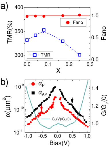
We begin by analyzing the electron transport and SN behavior at T=4K. The zero bias TMR as a function of V content shows a maximum (Fig.1(a)), confirming a reduction of the interface mismatch reported previously at room temperature Bonell2009 ; Herranz2010 ; Bonell2010 . The nearly Poissonian character of the tunneling statistics with Fano factor (Fig.1(a)) indicates nearly direct tunneling processes.
Figure 1(b) shows the bias dependence of the Hooge factor in both P and AP states for a Fe/MgO/Fe MTJ used as reference. One observes an excess LFN below 200 mV, where FeODu2010 and Fe/MgOTiusan2007 interface defect states have been predicted to influence the conductance. For the MTJ with a non-optimised Fe/MgO interface one observes a strong suppression of LFN with bias with weak anomalies in the around 0.5V, indicated by arrows.
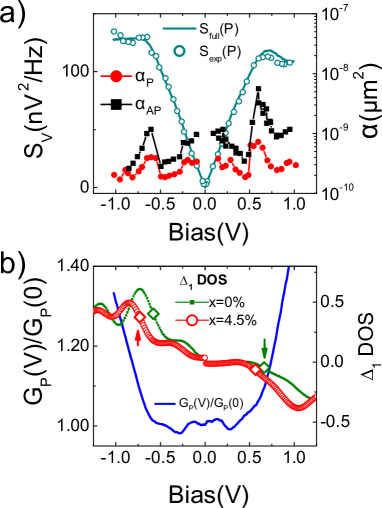
The doping of Fe with V improves the interface mismatch and decreases the Fe/MgO interface defect states density Bonell2009 ; Herranz2010 ; Bonell2010 , which allows the implementation of the BENS method. Figure 2(a) shows the and SN dependences for Fe0.96V0.04/MgO/Fe MTJs. The SN gives a Fano factor close to one, proving direct tunneling in the bias range under study (Fig.2(a)). In contrast to what is observed for the reference sample (Fig.1), the LFN shows a clear enhancement (factor of 2) of conductance fluctuations around . Yet a stronger enhancement of the LFN close to 0.6V is observed in AP configuration. The dynamic conductance in both states shows an upturn around 0.6V, but appears clearer in the P state (Fig.2, AP state not shown for simplicity). Numerical calculations of the tunneling electron DOS indicate that the upturn in conductance and the noise enhancement could be related with the opening of a new transmission channel when the Fermi level of one magnetic electrode crosses one of the band edges of the other magnetic electrode, indicated by arrows in Fig.2(b).
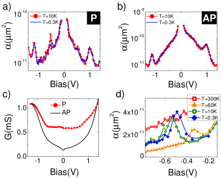
Even clearer signs of the band edges in LFN are seen with an 8% of V where the lowest background LFN and the maximum TMR (Fig.1) are achieved. Figure 3 shows dependence in Fe0.92V0.08/MgO/Fe MTJs were the optimum relation between two competing effects is reached: FM/I interface relaxation on the one side and still not essential suppression of the magnetization and the induced Fe-V structural disorder on the other side Bonell2009 ; Herranz2010 ; Bonell2010 . We estimate the TMR from our simulations using the Jullière model Julliere1975 (Fig.S.2) which indicates the optimum values are reached for 9% of V, i.e. rather close to what is experimentally observed. We have found that the Fe0.92V0.08/MgO/Fe MTJs show clear anomalies in the Hooge factor for biases around 1V and around 0.6V for the P state only, as shown in Fig. 3(a,b). Fig.3(d) demonstrates how the anomaly in the P state around 0.6V gradually disappears with temperature, probably due to thermal excitations.
Qualitatively similar effects were seen for Fe0.83V0.17/MgO/Fe and Fe0.75V0.25/MgO/Fe MTJs with the latter being the most robust to electrical breakdown (standing up to 2.5V). In the high V content range, the LFN is strongly influenced by random telegraph noise at positive biases around 1V, reflecting a strongest asymmetry in interface defect states previously visualized with scanning electron microscopy for Fe0.8V0.2/MgO/Fe MTJs Bonell2010 .
Fig.4(a) qualitatively explains the BENS method. As long as tunneling through the barrier is coherent, the main source for LFN are conductance fluctuations due to atomic defects affecting and interface states. Resulting localized states close to the band edges Fahy2006 could contribute, as reported for bulk semiconductors Jayaraman1989 ; Borovitskaya2001 , to the enhanced LFN. The key new feature of the BENS is the versatility in displacing the Fermi level ( in Fig.4(a)) of the ejector electrode with respect to the different band edges (or mobility edge, in Fig.4(a)) by simply varying the applied bias. The right panel shows how the conductance and its derivatives are expected to change when a new electron channel with a band edge opens at . In order to clearly detect inelastic relaxation through IETS, some well defined defect states should relax energy through coupling to a well-defined set of phonon energies. We believe that the random interface potential and the absence of well-defined defect states smear out the IETS signals. Tunneling to the band tail weakly influences IETS (insert of Fig.S.1(c)) reflecting only the derivative of the DOS close to . On the other hand, much stronger changes in LFN vs. bias are seen due to a strong change of excited defect relaxation times Borovitskaya2001 when tunneling close to , activating an excess of the low frequency conductance fluctuations. Therefore, interface defect states dominate the LFN, and not the derivative of the conductance (insert of Fig.S.1(c)).
The following arguments indicate that LFN mainly originates from disorder/defects close to the FM/I interface: (i) direct tunneling (Fig.1); (ii) the metallic nature of the electrodes, with resistance a few thousand times below the barrier resistance, ensuring that electric signals and their fluctuations mainly come from regions in the barrier and interfaces; (iii) by analyzing LFN at higher biases we avoid direct resonant excitation of localized FeO or O interface defect levels predicted below 200 mV Du2010 .
A simplified physical picture explaining the variation of LFN when tunneling to three different energies around (Fig.4(a) and Fig.S.1) is as follows. When electrons tunnel to energies their relaxation time is fast due to the delocalized character of the band states near with a correspondingly small contribution to LFN. For tunneling to electron states the LFN is also expected to be small due to low probability of these tunneling events. However, when electrons tunnel to the energies , the tunneling current could be affected by multiple trapping-type relaxations originating from shallow defect states contributing to the formation of the band edge tails. We estimate that the LFN peak width is roughly determined by the energy difference between the mobility edge and the bottom of the band tail.
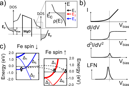
In the MTJs under study, electron tunneling mainly occurs between polarized bands with different Bloch state symmetries spin filtered by the MgO barrier Butler2001 ; Mathon2001 ; Bowen01 ; FVincent03 ; Parkin04 ; Yuasa04 . This allows a rough estimation of the interband mixing at the interface by analyzing variation of BENS response with relative alignment of the electrodes. Let us discuss qualitatively the reasons why BENS could provide LFN peaks both in the P and AP states (Figs. 2,3). For simplicity, we shall use the majority and minority Fe electron bands tunneling in Fe/MgO/Fe junctions (Fig.4(c)). When the MTJ is in the AP state, then in accordance with BENS arguments and band edge tunneling could provide a peak in LFN (AP) at different biases from 0.4 to 1.3 V if conductance fluctuations originate from elastic scattering events. Experimentally, however, we observe LFN peaks in the P state too (Fig.2(a)), which we link with the presence of spin-orbit coupling induced interband mixing at the Fe/MgO interface Lu2012 . Indeed, large lateral momentum transfer and interband scattering could be dominant only close to the interfaces Tsymbal2012 . Within such scenario, the relation between amplitudes of the peaks LFN(P)/LFN(AP) provides an evaluation of the degree of interband mixing between majority band and the minority of roughly 0.2-0.3.
In order to examine quantitatively the applicability of our model we have performed calculations of unit cell of Fe1-xVx /MgO (x=0, 0.045, 0.091, 0.182) with a 5 monolayers (ML) of MgO and 11 ML of Fe1-xVx. Our first-principles calculations are based on density functional theory (DFT) as implemented in the Vienna simulation package (VASP)vasp within the framework of the projector augmented wave (PAW) potentials paw to describe electron-ion interaction and generalized gradient approximation (GGA)gga for exchange-correlation interactions. A 13133 K-point mesh was used in our calculations. A plane wave energy cut-off equal to 500 eV for all calculations was used and is found to be sufficient for our system
Fig.5 compares the experimentally observed LFN anomalies in the P state (open dots) with the band edge positions (closed dots) estimated from inflection points in the DOS simulations for the majority and minority and states of Fe1-xVx/MgO (x=0, 0.045, 0.091, 0.182) structures (as indicated by arrows in the Fig.2(b)). We have also indicated by horizontal dotted lines the estimated positions of the band edges of the Fe/MgO structure.
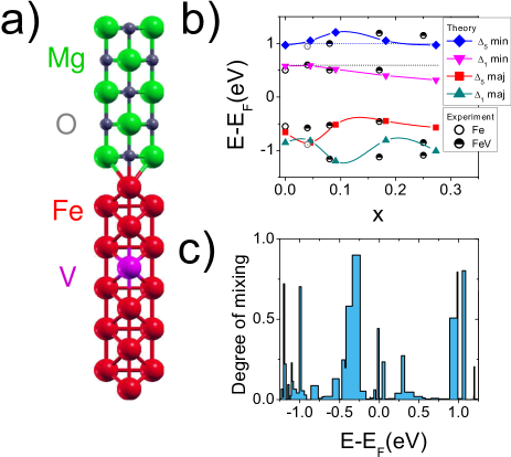
A reasonable agreement between simulations and the experiment is observed, especially for the Vanadium content between ( with reduced lattice mismatch, the lowest background LFN and the highest TMR.
A few factors could contribute to some difference between experimental results and calculations. First of all, calculations do not consider the presence of dislocation induced mismatch as well as the structural disorder difference between bottom and top interfacesBonell2010 . On the experimental side, measurements on MTJs with the least Vanadium were done below 1V due to their vulnerability, making them difficult to compare with the calculation results above 1V.
Finally, in order to better understand the influence of spin mixing at the interface, we have also analyzed the Bloch state character of the interfacial Fe atom in the presence of SOI as a function of the energy difference to . Fig.5(c) presents this analysis for and interface states in Fe0.909V0.091/MgO structure, mainly participating in the electron tunneling through MgO. When the degree of mixing at certain energy is equal to zero, it means that there is no mixing between different channels and there is only one Bloch state character that dominates the tunneling at this energy tunneling. The channel mixing is more pronounced at biases around and not above , i.e. close to the intervals where LFN anomalies of different magnitude were observed in both magnetic states (Fig.5(c)). We believe that and mixing could be due to surface induced band crossings and explains the appearance of peaks in LFN both in the P and AP states.
To summarize, we have introduced the band edge noise spectroscopy concept which permits an investigation of the electron band edges in a wide class of tunneling devices. We demonstrated successfully BENS approach in epitaxial magnetic tunnel junctions. The dependence of the BENS on the relative magnetic alignment of the electrodes allows us to estimate the importance of interband hybridization and spin flips at the FM/I interfaces. Given the crucial importance of buried interfaces in solid-state devices, the clear need to understand their electronic structure, and the limited options available, our work presents a substantial advance in the field of characterizing buried interfaces.
The authors acknowledge A. Gomez-Ibarlucea, D. Herranz and F. Bonell for their help with the experiments and sample growth. This work has been supported by the Spanish MINECO (MAT2012-32743) and Comunidad de Madrid (P2009/MAT-1726) grants.
References
- (1) H. Kroemer, Rev. Mod. Phys. 73, 783 ( 2001).
- (2) C Tiusan, et al, J. Phys.: Condens. Matter 19 165201 (2007).
- (3) S. Yuasa, D. D. Djayaprawira, J. Phys. D: Appl. Phys. 40 R337, (2007).
- (4) M. Z. Hasan, C. L. Kane, Rev. Mod. Phys., 92, 3045 (2010).
- (5) T. Schlenk, et al., Phys. Rev. Lett., 110, 126804 (2013).
- (6) K. D. Belashchenko, J. Velev, and E. Y. Tsymbal, Phys. Rev. B72, 140404R (2005).
- (7) L. D. Bell, W.J. Kaiser, Phys. Rev. Lett., 61, 2368 (1988).
- (8) F. Bonell, et al., Phys. Rev. Lett., 108, 176602 (2012)
- (9) R. F. Berger, C. J. Fennie, and J. B. Neaton, Phys. Rev. Lett., 107, 146804 (2011).
- (10) M. Jullière, Phys. Lett. 54A, 225 (1975).
- (11) J.S. Moodera, L.R. Kinder, T.M. Wong, R. Meservey, Phys.Rev.Lett. 74, 3273 (1995).
- (12) T. Miyazaki, N. Tezuka, J. Magn. Magn. Mat. 139, L231 (1995).
- (13) J. M. De Teresa, et al., Science, 286, 507 (1999).
- (14) W. H. Butler, X.-G. Zhang, T. C. Schulthess, and J. M. MacLaren, Phys. Rev. B63, 054416 (2001).
- (15) J. Mathon and A. Umerski, Phys. Rev. B 63, 220403(R) (2001).
- (16) M. Bowen, et al., Appl.Phys.Lett. 79, 1655 (2001).
- (17) J.Faure-Vincent, et al., Appl.Phys.Lett. 82 4507 (2003).
- (18) S.S.P. Parkin, et al., Nature Mat. 3, 862 (2004).
- (19) S. Yuasa, et al, Nature Mat. 3, 868 (2004).
- (20) D.A.Stewart, Nano Lett. 10, 263 (2010).
- (21) P.-J. Zermatten, et al., Phys. Rev. B78, 033301 (2008).
- (22) I. Rungger,1 O. Mryasov, S. Sanvito, Phys. Rev. B79, 094414 (2009).
- (23) T. Harada, et al., Phys. Rev. Lett. 109, 076602 (2012).
- (24) R. C. Jaklevic and J. Lambe, Phys. Rev. Lett. 17, 1139 (1966).
- (25) J. M. Teixeira, et al., Phys. Rev. Lett. 106, 196601 (2011).
- (26) D. Wortmann, H. Ishida, and S. Blügel, Phys. Rev. B72, 235113 2005
- (27) K. Nikolic and A. MacKinnon, Phys. Rev. B50, 11008 ( 1994),
- (28) G. Xu, et al., Nano Lett. 10, 4590, (2010).
- (29) P. Dutta and P.M. Horn, Review of Modern Physics, 53, 497 ( 1981).
- (30) F. Bonell, et al . IEEE Trans. Mag. 45, 3467 (2009).
- (31) D. Herranz, et al., Appl. Phys. Lett., 96, 202501 (2010).
- (32) F. Bonell, et al., Phys. Rev. B82, 092405 (2010).
- (33) R. Guerrero, et al., Phys. Rev. Lett., 97, 266602 (2006).
- (34) R. Guerrero, et al., Appl. Phys. Lett., 91, 132504 (2007).
- (35) G. X. Du, et al., Phys. Rev. B81, 064438 (2010).
- (36) S. Fahy, A. Lindsay, H. Ouerdane, E. P. O’Reilly. Phys. Rev. B74, 035203 (2006).
- (37) R. Jayaraman, C.G. Sadini, IEEE Transactions on Electronic Devices, 36, 1773 ( 1989).
- (38) E. Borovitskaya, M.S.Shur, Sol. St. Electronics, 45, 1067 (2001).
- (39) Y. Lu, et al., Phys. Rev. B86, 184420 (2012).
- (40) E.Y.Tsymbal and I. Zitic, Handbook on spin transport and magnetism, Ed., CRS Press, Taylor and Francis Group, 2012, p. 246.
- (41) Y. Ando, et al., Appl. Phys. Lett., 87, 142502 (2005).
- (42) G. Kresse and J. Hafner, Phys. Rev. B 47, 558 (1993); 54, 11169 (1996); Comput. Mater. Sci. 6, 15 (1996).
- (43) P. E. Blöchl, Phys. Rev. B 50, 17953 (1994); G. Kresse and D. Joubert, Phys. Rev. B 59 1758 (1999).
- (44) Y. Wang and J. P. Perdew, Phys. Rev. B 44, 13298 (1991).