Quantum Spin Hall Effect in IV-VI Topological Crystalline Insulators
Abstract
We envision that quantum spin Hall effect should be observed in -oriented thin films of SnSe and SnTe topological crystalline insulators. Using a tight-binding approach supported by first-principles calculations of the band structures we demonstrate that in these films the energy gaps in the two-dimensional band spectrum depend in an oscillatory fashion on the layer thickness. These results as well as the calculated topological invariant indexes and edge state spin polarizations show that for films 20–40 monolayers thick a two-dimensional topological insulator phase appears. In this range of thicknesses in both, SnSe and SnTe, (111)-oriented films edge states with Dirac cones with opposite spin polarization in their two branches are obtained. While in the SnTe layers a single Dirac cone appears at the projection of the point of the two-dimensional Brillouin zone, in the SnSe (111)-oriented layers three Dirac cones at points projections are predicted.
pacs:
71.20.-b, 71.70.Ej, 73.20.At, 79.60.-iTopological insulators (TIs) and the quantum spin Hall (QSH) effect attract significant interest for both fundamental and practical reasons. In the three-dimensional (3D) and two-dimensional (2D) TIs the bulk insulating states are accompanied by metallic helical Dirac-like electronic states on the surface (edges) of the crystal. Due to the time-reversal symmetry, these surface states are topologically protected against scattering at 180o. In 2D TIs this means that the metallic edge states provide dissipationless, spin-polarized conduction channels. Such property makes these structures extremely interesting for low-power-consumption electronics and spintronics. Thus, the quest for systems with topologically non-trivial edge states, which give rise to QSH effect, has become recently one of the most important topics in condensed matter physics.
The QSH effect is the net result of two opposite polarized spin currents traveling in opposite directions along the edges of a 2D TI. It has been predicted by Kane and Mele in graphene Kane1-PhysRevLett-2005 . In this material, however, it could occur only at unrealistically low temperatures, since the intrinsic spin-orbit coupling, which should open a band gap at the Dirac points, is very weak. Subsequently, it has been proposed and confirmed experimentally that QSH state might arise in HgTe/HgCdTe quantum wells Koenig-Science-2007 and also in InAs/GaSb heterostructures Knez_PRL-2011 . In these experiments the transition from insulating to conducting behavior has been observed. In both cases the conductivity was close to the value expected for the two parallel quantum Hall channels. The spin polarized nature of the edge states has been shown much later and only in the HgTe-based structure Brune-NaturePhys-2012 . All these observations were made at very low temperatures, below 10 K, due to the small energy gap in these systems.
In the search for new QSH structures many theoretical predictions have been made, in which various, sometimes exotic, chemical classes of 2D materials were considered. These include slightly buckled honeycomb lattice of Si atoms (silicene) Xing=Tao-An-APL-2013 , Bi bilayers on different substrates Zhi-Quan-PRB-2013 , Ge(BixSb1-x)2Te4 with various Bi concentrations Singh-PRB88-2013 and functionalized ultrathin tin films (stanene) Yong-Xu-PRL-2013 . Recently, it has been also shown that 2D transition metal dichalcogenides (Mo or W) should form a new class of large-gap QSH insulators Fu-2014 . Finally, a 2D TI with energy gap as large as 0.8 eV has been predicted for an overlayer of Bi grown on semiconductor Si(111) surface functionalized with one-third monolayer of halogen atoms PNAS-2014 . Despite all these theoretical predictions, no stand-alone thin film or a thin film supported on a suitable substrate have been up to now experimentally demonstrated to harbor a QSH state.
In this article we describe a study of -oriented thin films of well known IV-VI semiconductors SnSe and SnTe, which can be quite easily grown on a BaF2 substrate by e.g. molecular beam epitaxy. Such layers have rock-salt crystal structure, despite that bulk SnSe has an orthorhombic structure. private Recently, it has been shown that these compounds are so-called topological crystalline insulators (TCIs). TCIs are nontrivial insulators supporting surface Dirac fermions protected not by time-reversal but by crystal symmetry Fu-PhysRevLett-2011 . The IV-VI semiconductors, i.e., SnSe and SnTe, as well as PbTe and PbSe and the substitutional solid solutions of Pb- and Sn-based chalcogenides were identified earlier as trivial insulators. This is because in these compounds the band inversion happens simultaneously at an even number (four) of points in the Brillouin zone (BZ). The angle-resolved photoemission spectroscopy (ARPES) confirmed, however, that these materials belong to the TCI class. It has been shown that metallic surface states exist on the surfaces of SnTe Tanaka-NatPhys-2012 as well as Pb1-xSnxSe Dziawa-NatMater-2012 and Pb1-xSnxTe Xu-NatCommun-2012 . These gapless surface states are supported by mirror symmetry. It should be emphasized that due to the spin-orbit interactions the metallic surface states observed in real SnTe- or SnSe-based compounds have almost linear, Dirac-like dispersions. It has been shown lately that in (001)-oriented thin films of TCIs hybridization leads to a new 2D TCI phase, which supports two pairs of spin-filtered edge states Junwei-Liu-NatureMat-2014 ; Ozawa . These edge states are protected solely by mirror symmetry – the topological phase is indexed by the mirror Chern number . In contrast, our calculations show that in ultrathin TCI films (SnTe and SnSe) grown not along but along crystallographic axis, the QSH state can be obtained. This is because the four point projections onto the 2D BZ of a (111)-oriented thin film are not equivalent. While the energy structures at the three projections are the same by symmetry, the energy structure at the fourth projection at the point is different. This results in a possibility that the band inversion takes place in an odd (either one or three) number of points.
A IV-VI crystal in rock-salt structure has {111} planes alternately composed of either cations or anions. Thus, (111)-oriented slabs consisting of an even number of monolayers have one surface cation- and the other anion-terminated. In contrast, in slabs with an odd number of layers both surfaces are the same and the inversion symmetry is preserved. These two cases have to be distinguished.
I Odd number of monolayers
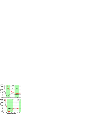
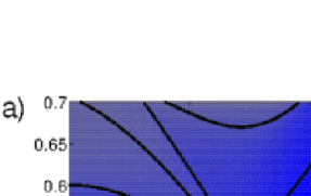
For a (111)-oriented SnTe or SnSe thick film four single, topologically protected Dirac-cones in the four projections of the -points onto the 2D BZ (one in point and three in the points) are obtained in the calculations. This is similar to what we have obtained before for a (111)-oriented bulk PbSnTe crystal Safai-PRB-2013 . For the anion-terminated surfaces, the bands are brought to contact forming anion Dirac cones, while in the other case the bands meet to form cation Dirac cones. As shown already in Ref. Safai-PRB-2013, ; Liu-PRB-2013, , all points belong to the three {110} mirror planes of the (111)-surface and all Dirac points should be thus topologically protected. This predictions have been also confirmed experimentally for (Pb,Sn)Se Creig as well as for SnTe Ando case. While at the point the Dirac-cone is isotropic, the band structure around is strongly anisotropic, i.e., depends differently on the values along the - and - directions. This is due to different orientations of the constant energy ellipsoids around different points: the ellipsoid is projected on along its long axis, whereas the ellipsoids for the other three points are inclined away from the projection direction. When the thickness of such TCI film decreases the gaps in the Dirac cones open, since the wave functions of the top and bottom surface states start to hybridize with each other. Examples of band structures around and around points in the 2D BZ of (111)-oriented SnTe(SnSe) thin films are presented in Fig. S1 (Fig. S2) in the Supplement. In Supplementary Section I the calculation method together with the obtained tight-binding parameters is also presented. Here in Fig. 1 we present the 2D state energy gaps in ultrathin cation-terminated (111)-oriented SnTe (a) and SnSe (b) slabs as a function of the number (odd) of monolayers in the film.
As shown in Fig. 1, in SnTe films the energy gap at the point decreases monotonically with the increase of the film thickness. At the point, however, damped oscillations of the energy gap with the number of monolayers can be observed. According to these results the first and biggest band gap inversion can be expected for SnTe films 3 - 6 nm thick, i.e., consisting of 17-33 monolayers. In contrast, in SnSe thin films energy gap at decreases monotonically, while the one at the point oscillates with the thickness of the film - in this case the first band gap inversion in should occur for films with 19-39 monolayers, what corresponds to similar thicknesses of 3.3 - 6.7 nm. Analogous results are obtained for the anion-terminated layers. In this case, however, due to the smaller range of anion wave functions the inverted band gap starts to occur for slightly thinner layers (2.4 - 5.3 nm for SnTe and 2.6 - 5.7 nm for SnSe), as shown in the Supplementary Section II. The damped oscillations of the band gap result from the corrections to the Dirac-like Hamiltonian of massive electron and have been already predicted for thin films of 3D TIs, like Bi2Se3 or Bi2Te3 Linder-2009 ; Lu-PRB81-2010 . In SnTe and SnSe terms are highly anisotropic. The differences in the results obtained for films of these materials stem from the fact that in SnTe the term moves the energy gap from towards the point, whereas in SnSe towards the point (see Fig. S3 in the Supplement).
In analogy to results obtained in Ref. Ozawa, for (001)-oriented Pb1-xSnxTe layers, the described above changes of the energy gaps are associated with a topological phase transition. Our calculations show, however, that in the case of (111)-oriented SnTe and SnSe layers the topological phase changes from trivial insulator not to TCI, but to the 2D TI. The effect is similar to the transition to 2D TI predicted for Bi2Se3 or Bi2Te3 thin films Lu-PRB81-2010 . This result is obtained by calculations of the invariant , which in 2D distinguishes between the trivial and QSH phase. For systems with inversion symmetry, i.e., for films consisting of an odd number of monolayers, the parity of the occupied bands eigenstates at the four time-reversal momenta points in the BZ (one and three ) determines the invariants Fu-PRB76-2007 . The green shadowed areas in Fig. 1 denote the SnTe and SnSe layer thicknesses, for which the value has been obtained by the prescription given in Ref. Fu-PRB76-2007, .
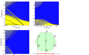
In Fig. 2a and 2b we present the calculated [] edge spectral functions of the (111)-SnTe cation-terminated film consisting of 19 monolayers (i.e., with inverted band gap – compare Fig. 1a). The results for a slab consisting of 13 monolayers, where a trivial insulator phase is expected, is presented in Fig. 2c. The 2D BZ zone of the (111)-oriented film and 1D BZ of the [] edge are presented in Fig. 2d. As shown in the latter, the and points project onto the edge at , while and at . In agreement with the results of topological invariant calculations, shown above, Dirac crossing of the edge states appears in the band gap at the projection for the 19-layers, but not for the 13-layers thick slab (compare Fig. 2a and 2c). At the projection of and (for ) the Dirac cones are not obtained for any SnTe layer thickness. In contrast, in SnSe, as shown in Fig. 3a and 3b for the anion-terminated 21-monolayer thick slab, two Dirac crossings of the edge states appear inside the band gap at the point. As the third point projects at , another edge state with a Dirac node appears at . Due to the strong band overlapping, the latter is dispersed within the valence band.
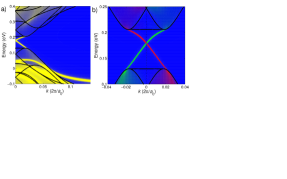
Finally, we have calculated the G↑ and G↓ contributions of the spin up and spin down (111)-projections in the edge spectral functions. The sign of the G↑ - G↓ difference corresponds to spin polarization of the edge states. As expected for the 2D TI in the QSH state, the obtained edge states are spin polarized and the spin polarizations in the two branches of the Dirac cones are always opposite. These spin polarizations in all studied cases are about 80%, i.e., the contribution of the dominant spin configuration surpasses ca 8-10 times the opposite spin orientation.
II Even number of monolayers
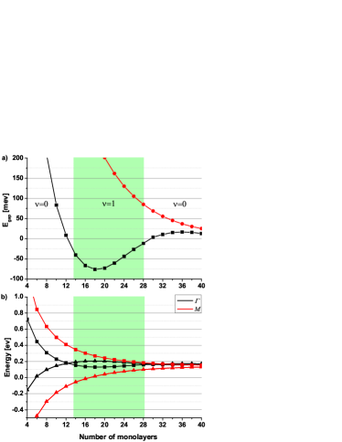
Unlike the case of an odd number of layers, for (111)-oriented slabs consisting of an even number of monolayers there is no inversion symmetry in the system and the energy gaps are moved from the time-reversal invariant points (see Figs S1(b) and S2(b) in the Supplementary Section I). The gap inversion occurs now in two points related by the time reversal symmetry on two sides of each time reversal invariant point. It has been shown for inversion-asymmetric systems in general Murakami-PRB-2007 that the gap closing can be accompanied by transition between the trivial insulator and the QSH phase when the gap inversion occurs in an odd number of such pairs. In SnSe films this takes place in three pairs in the vicinity of the three nonequivalent points while in SnTe in one pair around the point. Our calculations show that indeed for a given range of thicknesses the topological phase transition to the TI phase can be expected in these (111)-oriented films.
If there is no inversion symmetry in the system, the topological invariants can not be determined by the method utilizing the parity of the eigenfunctions, which we used for films with an odd number of monolayers. To calculate for such layers we have adopted the method proposed by Fukai and Hatsugai Fukai . In this method the improvements to computing Chern numbers in a lattice BZ enable the tight-binding calculations of based on the formula derived by Fu and Kane in Ref. Fu_Kane_2006, . The dependence of the band gap of SnTe (111)-oriented films consisting of an even number of monolayers on the layer thickness is shown in Fig. 4a. The thicknesses for which the value has been obtained are marked by the green shadow. As one can see in Fig. 4a the QSH phase can be expected in SnTe films consisting of 14-28 monolayers ( 2.5 - 5.1 nm thick). For SnSe the QSH phase is obtained for 18-38 monolayers, i.e., for film thicknesses in the range 3.1 - 6.6 nm. In the case of SnTe films with even number of layers the whole inverted energy gap for states in the vicinity of is situated inside the large gap between conduction and valence bands close to the point, as one can clearly see in Fig. 4b. The largest value of the inverted gap, about 75 meV, is obtained for the 18-20 monolayers thick SnTe slab.
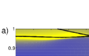
The calculated spectral functions along the [] edge for the (111)-oriented, 18-monolayers thick SnTe film show a clear Dirac node in the center of the band gap at the point. This is shown in Fig. 5a. The obtained results are in full agreement with the formalism developed in Ref. Murakami-PRB-2007, . We note that a similar result has been obtained for graphene Kane1-PhysRevLett-2005 – in this case one observes a single edge state with a Dirac node at (time-reversal symmetry point), despite the energy gaps appear in two points (in which the time-reversal is not preserved).
Fig. 6 presents the edge spectral functions at the projections of points at (a) and (b) point, calculated for the 20-monolayers thick SnSe slab. As shown in the Supplementary Material, in this case the band gap at the is very small. Still, a pair of edge states can be seen near the top of the valence band. The spin polarization of this edge state is shown in Fig. 6c. At the point, however, the edge states which form the two Dirac cones do not crossover the band gap to connect the valence and conduction bands. Instead, the upper and lower edge states repel each other and two anticrossings appear (see Fig. 6b). Interestingly, these edge states are still spin polarized, as shown in Fig. 6d.
The calculations presented above show that in the free standing (111)-oriented SnSe and SnTe thin films there exists a range of thicknesses for which the 2D TI phase appears. The QSH phase is obtained for all studied films, both with odd and also even number of monolayers. However, for all but the (111)-oriented SnTe films with an even number of monolayers an overlapping of bands in and diminishes the final band gap. Hence, the edge states appear either against the background of the bands or within a very small energy gap (see Supplementary Section II). The (111)-oriented SnTe films with an even, close to 20, number of monolayers is thus the best candidate for observing the QSH effect in the IV-VI TCI. The QSH phase produced in this material system is highly robust, being even oblivious to the lack of inversion symmetry. The latter indicates that a suitable substrate or an overlayer will not destroy this 2D TI phase. Quite the contrary, using carefully selected substrate or overlay material (e.g., Pb1-xEuxSe1-yTey quaternary alloy) would allow to tune the height of the energy barriers and biaxial strain in the structure Springholz . As shown already in Ref. Druppel, for SnTe (001) surface and for SnTe nanomembrane in Ref. Qian-NanoResearch-2014, , the uniaxial or biaxial strain can be used for manipulating with the energy gaps in the surface (or interface) states. The strain can be also used for solving the mentioned above problem of band overlapping, which diminishes the resulting energy gap (as it was shown in Ref. Buczko, for solving a similar obstacle in PbTe/(Pb,Sn)Te heterostructures). Thus, these results may pave the road for experimental realization of QSH in SnTe and SnSe layers and their quantum well structures.
III Acknowledgments
We would like to thank Tomasz Story, Moty Heiblum, Junwei Liu and Pawel Potasz for valuable comments and suggestions. This work is supported by the Polish National Science Center (NCN) Grants No. 2011/03/B/ST3/02659 and 2013/11/B/ST3/03934. PK wishes to acknowledge the support of the Weizmann Institute Visiting Scientist Program. Calculations were partially carried out at the Academic Computer Center in Gdansk, using resources provided by Wroclaw Centre for Networking and Supercomputing (http://wcss.pl), grant No. 330 and at Interdisciplinary Centre for Mathematical and Computational Modelling (ICM) of the University of Warsaw under a grant No. G51-18.
IV Contributions
S.S. performed band-structure calculations, within both tight-binding and ab initio approaches, with contributions and supervision from R.B. M.G. performed the calculations of topological invariants and spin polarization. P.K. and R.B. performed the theoretical analysis and wrote the manuscript, with contributions from all authors. R.B. conceived and supervised the project. All correspondence should be addressed to R.B.
References
- (1) Kane, C. I. & Mele, E. J. Qauntum Spin Hall Effect in Graphene. Phys. Rev. Lett. 95, 226801 (2005).
- (2) Konig, M. et al. Quantum Spin Hall Insulator State in HgTe Quantum Wells. Science 318, 766 (2007).
- (3) Knez, I., Du, R.-R. & Sullivan, G. Evidence for Helical Edge Modes in Inverted InAs/GaSb Quantum Wells. Phys. Rev. Lett. 107, 136603 (2011).
- (4) Brne Ch. et al. Spin polarization of the quantum spin Hall edge states. Nature Phys. 8, 485 (2012).
- (5) An, X.-T., Zhang, Y.-Y., Liu, J.-J. & Li, S.-S. Quantum spin Hall effect induced by electric field in silicene. Appl. Phys. Lett. 102, 043113 (2013).
- (6) Huang, Z.-Q. et al. Nontrivial topological electronic structures in a single Bi(111) bilayer on different substrates: A first-princiles study. Phys. Rev. B 88, 165301 (2013).
- (7) Singh, B., Lin, H., Prasad, R., & Bansil, A. Topological phase transition and two-dimensional topological insulators in Ge-based thin films. Phys. Rev. B 88, 195147 (2013).
- (8) Xu, Y. et al. Large-gap Quantum Spin Hall Insulators in Tin Films. Phys. Rev. Lett. 111, 136804 (2013).
- (9) Qian, X., Liu, J., Fu, L. & Li, J. Quantum Spin Hall Effect and Topological Field effect transistor in two-dimensional transition metal dichalcogenides. Preprint at http://arXiv.org/abs/1406.2749 (2014).
- (10) Zhou, M. et al. Epitaxial growth of large-gap quantum spin Hall insulator on semiconductor surface. PNAS 111, 14379 (2014).
- (11) Story, T., private communication.
- (12) Fu, L. Topological Crystalline Insulators. Phys. Rev. Lett. 106, 106802 (2011).
- (13) Tanaka, Y. et al. Experimental realization of a topological crystalline insulator in SnTe. Nature Phys. 8, 800 (2012).
- (14) Dziawa, P. et al. Topological crystalline insulator states in Pb1-xSnxSe, Nature Mater. 11, 1023 (2012).
- (15) Xu, S.-Y. et al. Observation of a topological crystalline insulator phase and topological phase transition in Pb1-xSnxTe. Nat. Commun. 3, 1192 (2012).
- (16) Liu, J. et al. Spin-filtered edge states with an electrically tunable gap in a two-dimensional topological crystalline insulator. Nature Mater. 13, 178 (2014).
- (17) Ozawa, H., Yamakage, A., Sato, M. & Tanaka, Y. Finite-size-effect-induced topological phase transition in a topological crystalline insulator. Phys. Rev. B 90, 045309 (2014).
- (18) Safaei, S., Kacman, P. & Buczko, R. Topological crystalline insulator (Pb,Sn)Te: Surface states and their spin polarization. Phys. Rev. B 88, 045305 (2013).
- (19) Liu, J., Duan, W. & Fu, L. Two types of surface states in topological crystalline insulators Phys. Rev. B 88, 241303(R) (2013)
- (20) Polley, C. M. et al. Observation of topological crystalline insulator surface states on (111)-oriented Pb1-xSnxSe films. Phys. Rev. B 89, 075317 (2014).
- (21) Tanaka, Y. et al. Two types of Dirac-cone surface states on the (111) surface of the topological crystalline insulator SnTe. Phys. Rev. B 88, 235126 (2013)
- (22) Linder, J., Yokoyama, T. & Sudbø, A. Anomalous finite size effects on surface states in the topological insulator Bi2Se3 Phys. Rev. B 80, 205401 (2009).
- (23) Lu, H.-Z., Shan, W.-Y., Yao, W., Niu, Q. & Shen, S.-Q. Massive Dirac fermions and spin physics in an ultrathin film of topological insulator. Phys. Rev. B 81, 115407 (2010) and refereces therein.
- (24) Fu L. & Kane C. L. Topological insulators with inversion symmetry. Phys. Rev. B 76, 045302 (2007).
- (25) Murakami, S., Iso, S., Avishai, Y., Onoda, M. & Nagaosa, N. Tuning phase transition between quantum spin Hall and ordinary insulating phases. Phys. Rev. B 76, 205304 (2007).
- (26) Fukui, T. & Hatsugai, Y. Quantum Spin Hall Effect in Three Dimensional Materials: Lattice Computation of Topological Invariants and Its Application to Bi and Sb. J. Phys. Soc. Jpn 76, 053702 (2007).
- (27) Fu, L. & Kane, C. L. Time reversal polarization and a adiabatic spin pump. Phys. Rev. B 74, 195312 (2006).
- (28) Springholz, G. & Bauer, G. IV-VI Semiconductors, in: K. Klingshirn (Eds.): Semiconductor Quantum Structures: Growth and Structuring, Volume III, Number 34A, Pages 415-561, (Springer, Berlin, 2013).
- (29) Drüppel, M., Krüger, P. & Rohlfing, M. Strain tuning of Dirac states at the SnTe (001) surface. Phys. Rev. B 90, 155312 (2014).
- (30) Qian, X., Fu, L. & Li, J. Topological crystalline insulator nanomembrane with strain-tunable band gap. Preprint at http://arxiv.org/abs/1403.3952 (2014)
- (31) Buczko R. & Cywiński Ł. PbTe/PbSnTe heterostructures as analogs of topological insulators. Phys. Rev. B 85, 205319 (2012).