Characterization studies of Silicon Photomultipliers and crystals matrices for a novel time of flight PET detector
Abstract
This paper describes the characterization of crystal matrices and silicon photomultiplier arrays for a novel Positron Emission Tomography (PET) detector, namely the external plate of the EndoTOFPET-US system. The EndoTOFPET-US collaboration aims to integrate Time-Of-Flight PET with ultrasound endoscopy in a novel multimodal device, capable to support the development of new biomarkers for prostate and pancreatic tumors. The detector consists in two parts: a PET head mounted on an ultrasound probe and an external PET plate. The challenging goal of 1 mm spatial resolution for the PET image requires a detector with small crystal size, and therefore high channel density: 4096 LYSO crystals individually readout by Silicon Photomultipliers (SiPM) make up the external plate. The quality and properties of these components must be assessed before the assembly. The dark count rate, gain, breakdown voltage and correlated noise of the SiPMs are measured, while the LYSO crystals are evaluated in terms of light yield and energy resolution. In order to effectively reduce the noise in the PET image, high time resolution for the gamma detection is mandatory. The Coincidence Time Resolution (CTR) of all the SiPMs assembled with crystals is measured, and results show a value close to the demanding goal of 200 ps FWHM. The light output is evaluated for every channel for a preliminary detector calibration, showing an average of about 1800 pixels fired on the SiPM for a 511 keV interaction. Finally, the average energy resolution at 511 keV is about 13 %, enough for effective Compton rejection.
1 Introduction
Positron Emission Tomography (PET) is a non invasive, diagnostic
imaging technique for measuring the metabolic activity of cells in the
human body. Nowadays it is widely used for cancer diagnosis
[1].
Among the tumors, pancreatic carcinoma is one of the most aggressive
and resistant to current therapies [2], and most often is detected only on
an advanced state of development. On the other hand, prostate cancer is
the most common cancer among males [3].
Both pancreas and prostate are surrounded by organs with high uptake:
the liver and the heart are close to the pancreas
while the bladder is near the prostate. In these cases the current
full-body multimodal PET scanners have strong limitations, due to the
noise from the neighboring organs and the lack of specific biomarkers
[4] [5].
EndoTOFPET-US [6] aims to overcome these limits, allowing to investigate the performances of newly developed
specific biomarkers of tumoral processes for pancreas and
prostate. Both organs are usually examined with ultrasound probes through natural cavities, therefore
the diagnostic capability can be enhanced by fusing the morphological
image from ultrasound with a PET metabolic image. The endoscopic
approach and the use of the TOF information with an unprecedented CTR of 200 ps (3 cm along the line of response) allow to
define a specific Region Of Interest (ROI) and
significantly suppress the background from the neighboring organs.
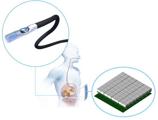
The EndoTOFPET-US detector consists of a PET head extension mounted on a
commercial US endoscope placed close to the ROI and an external PET
plate facing the patient’s abdomen, in coincide with the PET head
(Figure 1).
The external plate is a square of 23 x 23 cm2, and it is made of 256
detector unit modules. Each module consists in a 4x4 LYSO:Ce crystal
matrix glued to a discrete array of 4x4 analog SiPMs from Hamamatsu.
LYSO:Ce crystals have high light yield and fast decay time, therefore
appropriate for TOF PET.
SiPMs are novel photon detectors also suitable for TOF PET applications [7], thanks to their compactness, high gain,
insensitivity to magnetic fields, low operating voltage and excellent
timing properties.
The following sections describe the experimental setups and the results of the
characterization of the SiPMs, crystals and the combined system
(SiPM + crystal). All the setups have been designed for a fast and
reliable measurement of a large quantity of components, rather than a
detailed study of single devices.
2 Photodetector Characterization
The SiPMs chosen for the external plate are matrices of 4x4 discrete MPPCs (Multi Pixel Photon Counter) from Hamamatsu photonics (S12643-050CN). Each SiPM in the matrix is a square of 3.0 x 3.0 mm2 with 3464 active pixels (50 x 50 m2 each). The distance between two adjacent SIPMs in the matrix (center to center) is 3.6 mm. These SiPMs exploit the Through Silicon Via (TSV) technology, leading to less dead space and a reduced connection length as compared to conventional wire-bonded SiPM. The following sections describe the experimental setup, the analysis method and the results of the characterization of 256 SiPM matrices.
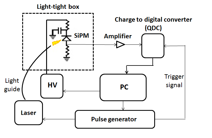
2.1 Experimental setup
The layout of the experimental laboratory setup is shown in Figure 2. In a light tight box, the SiPM matrix is mounted on a motherboard
incorporating linear amplifiers (Infineon BGA614) and high voltage
filters. The signal for each of the 16 SiPMs of the matrix is obtained using low intensity blue light (Advanced laser diode
system, 451 nm). The amplified SiPM output is readout by a VME-based
charge-to-digital converter (CAEN QDC965A) with a resolution of 25 fC
per QDC bin. The heat generated by the active components on the SiPM
motherboard is dissipated by a fan. The temperature is monitored by a
sensor (Dallas DS18B20) but not actively controlled.
2.2 Gain and Breakdown voltage
The integrated charge spectrum given by the light pulses in shown in Figure 3. This is repeated for 30 voltage steps, acquiring 200k events sample per step with an integration gate of 100 ns synchronized with the laser pulse. The first peak corresponds to the pedestal (zero pixel fired) while the following peaks correspond to an increasing number of pixels fired. After the pedestal subtraction, the spectrum is projected into the frequency space using a Fast Fourier Transform. The period of the first harmonic is taken as the value of the SiPM gain () in QDC units, which is then converted into number of electrons by the following formula:
| (1) |
where is the QDC resolution of 25 fC per QDC bin and is
the amplification factor of the readout board (19 dB, 8.9).
The error on the gain is about 1%, obtained as one bin in the Fourier space plus an
additional uncertainty of 5 , evaluated by repeating the measurement multiple times under the same conditions.
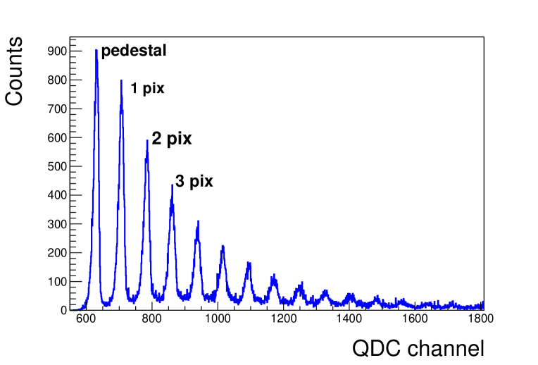
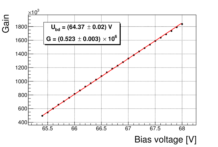
Figure 4 shows the gain dependence on the voltage bias applied. As expected, the gain is linearly proportional to the bias voltage applied, according to
| (2) |
where is the pixel capacitance, is the excess bias voltage,
is the applied bias voltage and is the breakdown
voltage. Hence is obtained by applying a linear fit and
extrapolating to zero gain, with an uncertainty of the order of a few
tens on mV.
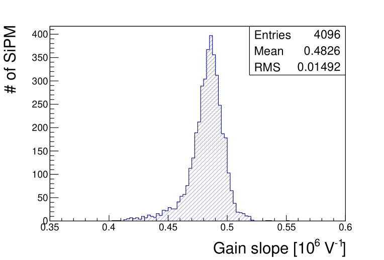
Figure 5 shows the distribution of the gain slope (
at 1 V excess bias) for all the SiPMs. The mean value is
0.48106 V-1 with a spread of 3% among the SiPMs tested.
It is known that the depends on the temperature
[8], and some fluctuations have occurred during the whole
set of measurements. Moreover, local differences in temperature have
been observed within the SiPM matrix, due to the inhomogeneous
dissipation of the heat generated by the amplifiers. Therefore an
offline temperature correction (see section 2.5) has
been applied in order to compare the results.
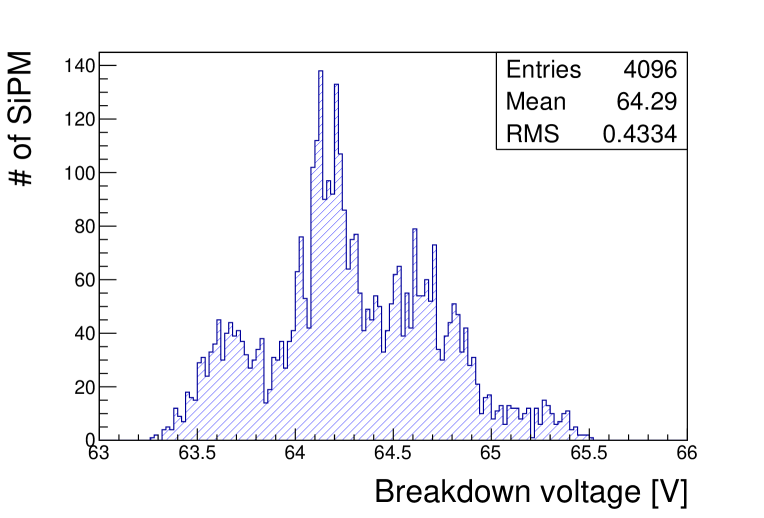
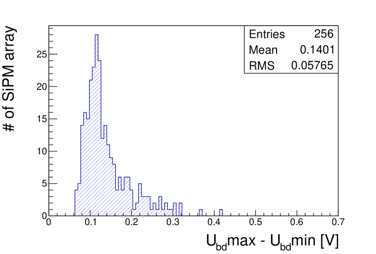
Figure 6 shows the distribution of the breakdown voltages
at 25 ∘C for all the SiPMs.
Although the spread for all the SiPM is about 2 V, this must
not exceed 0.5 V in each single SiPM matrix, because this is the
maximum voltage bias tuning range of the ASIC developed for the SiPM
readout [9] [10].
As shown in Figure 7, all the SiPM matrices respect this
requirement.
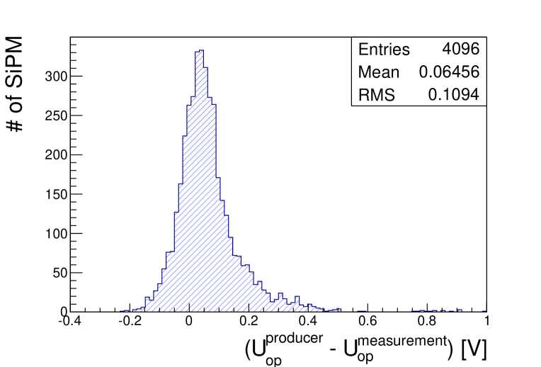
Finally, the results obtained have been compared to the operating
voltages () provided by the SiPM producer. The is
defined as: .
The differences between the calculated using equation
2 with data from the measurements and provided by
Hamamatsu are shown in Figure 8. The agreement is good,
despite a shift of 6% and a spread of 10%. This is due to the
different measurement method implied by the SiPM producer and the uncertainty of and .
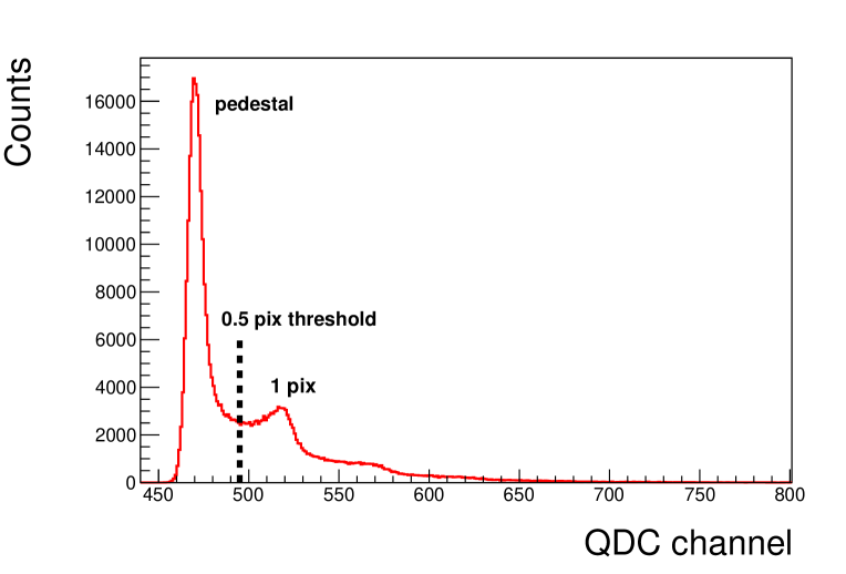
2.3 Dark Count Rate
Even in absence of light, an avalanche breakdown can be triggered by a
photoelectron generated from thermal excitation or by tunneling
effect. This phenomenon, usually called Dark Count Rate (DCR), is Poisson distributed and it is measured by randomly integrating the charge with
a time window of 100 ns (same time window as for the gain measurement). A typical noise spectrum is visible
in Figure 9.
The probability of having two dark events in the time is
very low, therefore the events corresponding to more than 1 pixel
fired are mainly due to correlated noise, which will be described in
the next section.
The events in the pedestal peak, i.e. the events with charge less than
0.5 pixel threshold, are not affected by correlated noise, hence they
are used to calculate the uncorrelated DCR, defined as .
In a time range , the expected number of events is given by . The number of events in the
pedestal distribution is given by the Poisson probability density
function for zero events in the time :
| (3) |
The is therefore calculated using:
| (4) |
where is the number of events in the pedestal peak and
is the total number of events recorded.
The error on the calculated value depends on the statistic of the
sample and on the quality of the spectrum.
For each SiPM the is evaluated for 30 voltage levels, in a range
of 3 V starting about 1 V above the breakdown voltage. 500k
event samples are collected for each voltage point.
Also the DCR has a dependence on the temperature, therefore a correction
(see section 2.5) has been applied in order to
compensate for temperature variations.
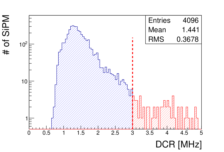
The distribution of , corrected to 25 ∘C and at 2.5 V excess
bias, is shown in Figure 10 for all the SiPMs.
The DCR has a negative impact on the time resolution. The best time
resolution is achieved when the timing threshold on the readout ASIC
is set as low as possible, up to the noise level.
Therefore a acceptance limit
of 3 MHz for each SiPM has been agreed with the SiPM producer.
Almost all the SiPMs are within the limit, however 5 matrices have been sent back to the producer because they
included at least one SiPM with excessive .
2.4 Correlated noise
Correlated noise includes after-pulse
and inter-pixel optical crosstalk [11].
After-pulses are generated if an electron produced during an avalanche
is trapped and released at a later time, with a delay ranging from nanoseconds
up to several microseconds. Depending on the trapping time constant and the pixel
recovery time, trapped electrons can generate an avalanche of equivalent or smaller charge with respect to the DCR pulses.
Inter-pixel crosstalk is due to optical photons generated during a
pixel breakdown. These photons have a certain probability to reach the
neighboring pixels, triggering new avalanches.
The precise measurement of each of the two effects is beyond the scope of
this study. However, it’s possible to estimate the correlated noise
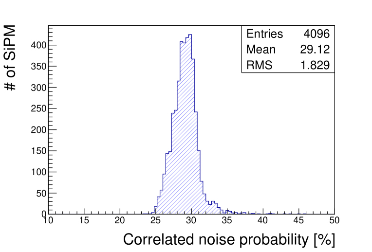
triggering probability as:
| (5) |
where is calculated by setting the threshold to 1.5 pixel fired. Figure 11 shows the correlated noise probability at 2.5 V excess bias for all the SiPMs. The average results obtained, about 30%, is compatible with measurements on similar devices and does not represent an issue for the detector operation.
2.5 Temperature dependence
As mentioned in previous sections, SiPM properties depend on
temperature. Therefore, DCR, gain, breakdown voltage and correlated
noise have been measured at different temperatures for a single SiPM in an array.
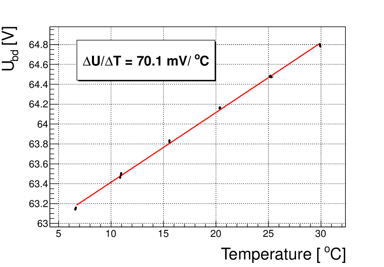
Using a climate chamber (Espec LU-123), several voltage scans
have been performed in a temperature range between 6 ∘C and 30 ∘C.
Figure 12 shows the linear temperature dependence of the
breakdown voltage; the uncertainty on the temperature is included but
it is smaller than the marker size. The coefficient obtained from the
linear fit is 70.1 mV/∘C, and is used for the temperature corrections applied in
section 2.2 and 4.1.
The dependence of the DCR as a function of the temperature should
scale with the density of the thermal carriers [12] according to equation:
| (6) |
where is the pixel capacitance, is the temperature of
the SiPM in Kelvin, is the activation energy and
is the Boltzmann constant.
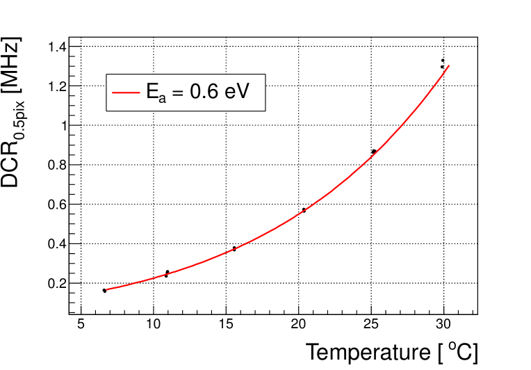
Figure 13 shows the DCR as a function of temperature at
2.5 V excess bias. An activation energy =0.6 eV is obtained by
fitting the data with equation 6. This value is compatible to previous studies [13], and it has been used for the temperature corrections applied in section 2.3.
The change in the gain is found to be less than C,
which is negligible for the temperature variations occurred during the
gain characterization of all the SiPMs. Also the correlated noise
shows a mild dependence on the temperature, but it is not relevant for
the detector performances.
3 Crystals characterization
The crystals for the external plate are grouped in 256 matrices of 4x4 LYSO:Ce
scintillators, produced by Crystal Photonics Inc. The volume of each crystal is 3.5x3.5x15 mm3 and within the matrix they are separated by a reflector foil (ESR Vikuiti by 3M). In order to ensure the system uniformity, measurements of light output and
energy resolution have been performed on both faces for each matrix using the MiniACCOS
setup [14], which allows a fast, automatic and highly reproducible data
acquisition process.
In this setup, each matrix is placed on a custom made teflon plate, for a total of 25 matrices
per plate. An air gap of 5 mm is left between the matrix face and the
PMT window.
Systematic measurements were performed to evaluate uncertainties arising from the bench, yielding a
total relative error of 4.7% for the light output and 12.8% for the
energy resolution.
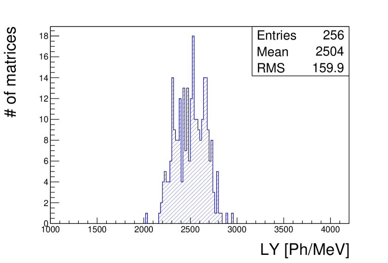
Figure 14 shows the distribution of light yield obtained with MiniACCOS setup for all the 256 matrices. The distribution spread is 6.4%, which subtracting the uncertainty of the setup gives a 4.3% as
light output dispersion. Figure 15 shows the
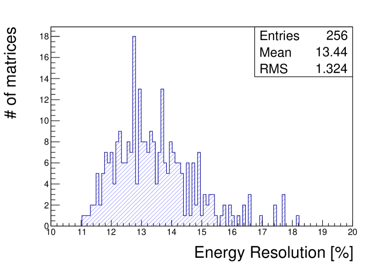
distribution of the energy resolution for all the modules, with a mean
value of 13.4%. The spread is comparable to the bench uncertainty, therefore the variations in
energy resoluton are just due to the setup.
In the final configuration, each matrix will be glued to a SiPM array. The absolute values of light
output obtained with the MiniACCOS setup have therefore to be rescaled to this configuration.
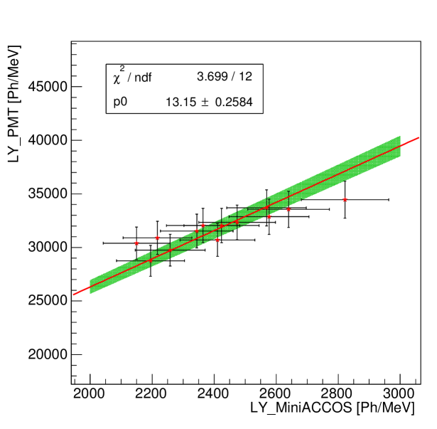
In order to obtain this, light output for a subset of 13 matrices was measured on a standard
XP2020Q PMT, using Rhodosil 47V grease as optical coupling and teflon
as back wrapping. The scaling factor between this measurement condition and MiniACCOS was
found to be 13.15, with a correlation coefficient of 0.89 between the two data sets, as shown in
Figure 16.
The average light yield for all the crystal matrices can therefore be derived as 32500
2700 Ph/MeV, including in the evaluation of the uncertainty also the systematics arising from
the calibration process.
Based on the studies reported in [15], it can be estimated that at least 20000 25000 Ph/MeV are necessary to achieve a CTR
of 200 ps FWHM, which make our set of matrices perfectly suitable for this purpose. The homogeneity on the crystals performance is also ensured within a 4.3% level for all 256 matrices
tested with an energy resolution of 13.4 1.3% as mean value.
4 Detector Module Characterization
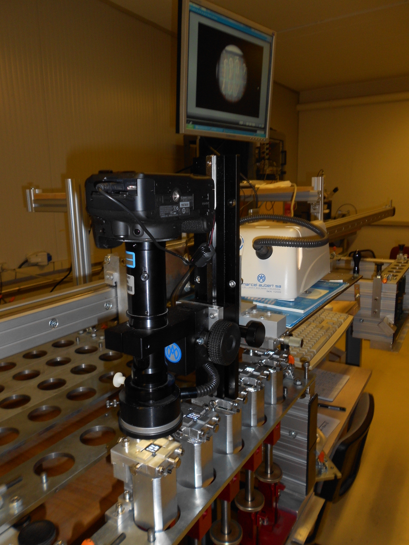
A dedicated bench has been developed to glue the crystal matrices on
the SiPM arrays, allowing to assemble 5 modules per day.
Figure 17 shows the setup: the crystal matrices are placed on a
movable support and a camera allows the visual alignment with the
SiPM matrices located under the crystals. The amount of glue (RTV3145)
is calculated in order to have a maximum thickness of 0.1 mm, and it is
spread over the SiPM matrix with a dispenser. The SiPM matrix is then
pushed againts the crystals and a visual inspection is performed to check
if any air bubble occurred. If none, the modules are left on the support for the curing time (24 h).
Every module is then measured regarding light output, energy
resolution and CTR, which are described in the next sections.
4.1 Detector light output
The detector light output for the 511 keV photon (defined here as ) is of primary importance for the detector time
resolution. As demonstrated in other studies [15], the number
of detected photoelectrons must be maximized in order to achieve the
best time resolution. Moreover, all the channels should have the same
response for the 511 keV photon, allowing an easier detector
calibration.
A source with an activity of about 1 MBq is used as a
emitter. The setup is similar to the one described in section
2.1 but the SiPM signal is not amplified and the
resolution of the QDC is set to 200 fC. The charge integration gate is set to 450 ns and it is triggered by the SiPM signal
itself, using a discriminator (CAEN model 96) and a gate generator
(LeCroy model 222). A channel switcher (Keithley 7002 switch system) provides automatic scan through the 16
channels in each matrix. The temperature is recorded before each
channel measurement. Each SiPM is operated at as defined in section 2.2, eventually corrected for temperature variations
according to the coefficient of 70.1 mV/∘C (see section 2.5).
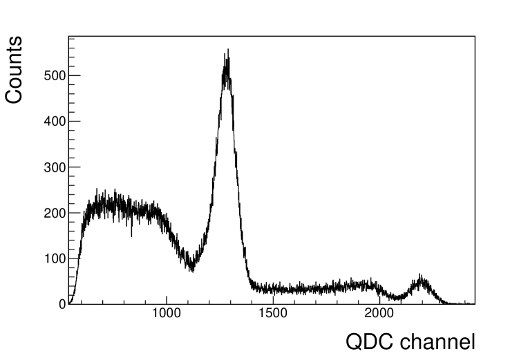
Fig 18 shows a typical spectrum for a single channel. The peak corresponding to the 511 keV photon in the charge spectrum is fitted by a Gaussian function. Hence the light output , expressed in number of pixels fired on the SiPM, is obtained by the following relation:
| (7) |
where is the mean value of the Gaussian fit, is 200 fC
per bin, is the pedestal position, and is 1.25x.
The uncertainty on , of the order of about 30 pixels, is
given by statistical error and temperature uncertainty of 0.5 oC. No error for
the is available.
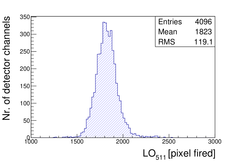
The light output distribution for all the channels is shown in
Figure 19, the average value of about 1800 pixels should
allow to reach the CTR of 200 ps FWHM.
A preliminary detector calibration will be based on these measurements.
4.2 Inter channel cross-talk
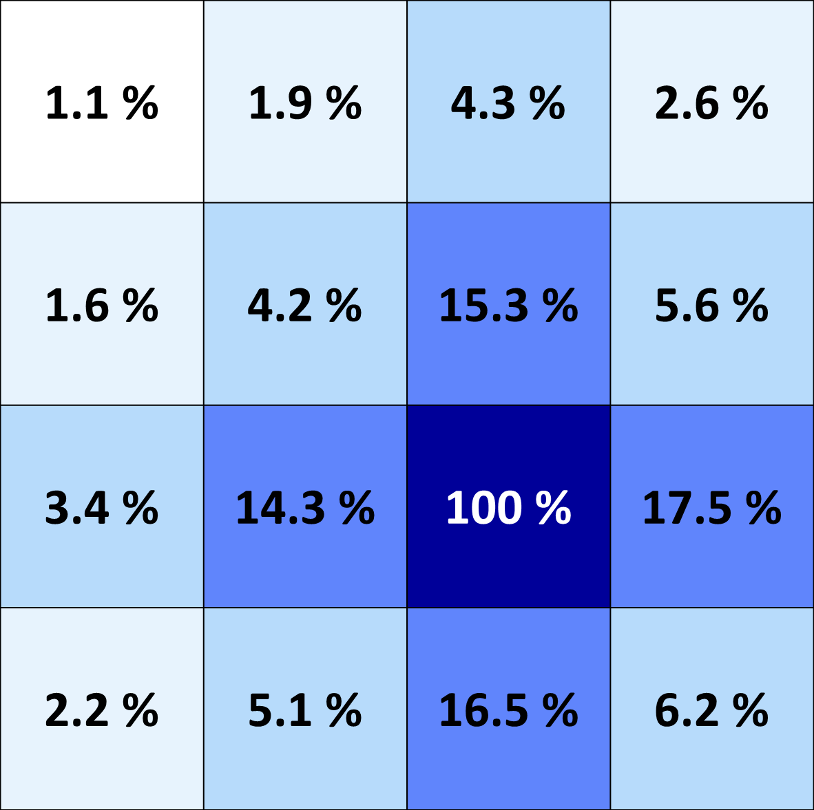
The cross-talk between the module channels is measured on a sample module.
Similarly to the setup described in section 4.1, the source is placed in front of the module and only one channel is chosen as trigger. Any other channel in the module is acquired simultaneously to the trigger, using a common integration gate of 450 ns in the QDC. The channel switcher provides the automatic scan trough the 15 channels, each operated at its own .
In every channel, only the events corresponding to the photopeak in the trigger are selected. Therefore, dividing the mean charge of these events by the photopeak position in the trigger, the cross-talk for the 511 keV photon is obtained for all the remaining 15 channels in the module.
The measurement is repeated by selecting different trigger channels in the module. Figure 20 shows the average crosstalk obtained from 4 different measurements: every time one of the central channels in the module is used as a trigger. The cross-talk does not exceed 20%, and can be suppressed by setting a threshold at 100 keV.
4.3 Energy calibration
It is well known that the SiPM is a non-linear device due to the
limited number of pixels, therefore a non-linear correction is
necessary in order to estimate the energy resolution for the 511 keV
gamma.
Using the setup described in section 4.1, the detector light output is measured for different
gamma energies: 356 keV from 133Ba, 511 and 1277 keV from 22Na, and
662 keV from 137Cs.
The measurement is performed on a sample of 4 modules (64 channels):
for each channel the light output data are fitted with the
function describing the SiPM saturation:
| (8) |
where is the average number of pixels fired on the photodetector,
is the number of pixel fired on the SiPM per unit of
energy deposited in the crystal and is the energy of the
detected gamma photon. is related to the maximum number of pixels in the SiPM. This
number is actually higher than the nominal value (3464 pixels) because
the pixel recovery time is about 20 ns, which is half of the decay
constant of the crystal (40 ns).
Figure 21 shows the non-linear function for one channel,
however this function is not unique for all the channels.
It is expected that the parameter varies among the channels
according to , which takes into account the variations in
the SiPM properties (photo detection efficiency, correlated noise),
crystal light yield and the optical coupling.
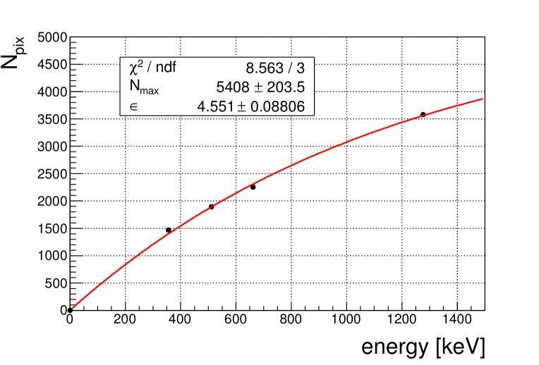
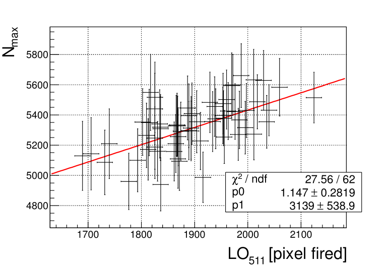
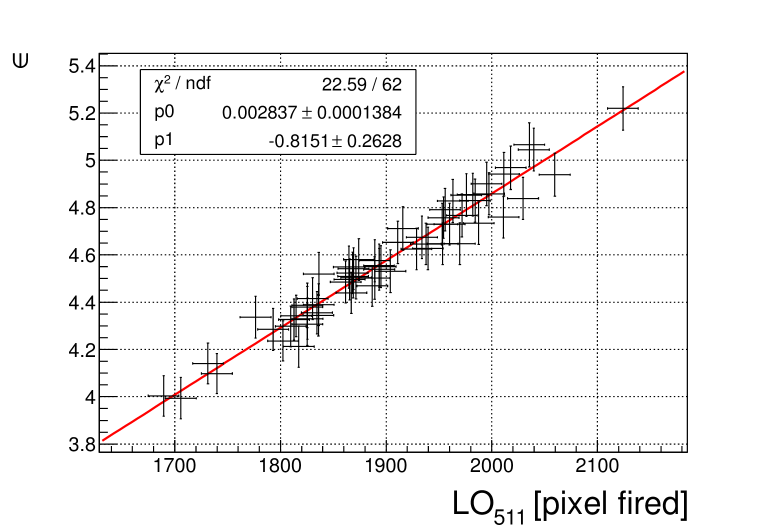
The dependence of and to the for the 64
channels is shown in Figure 22 and 23 respectively. Although the linear
dependence of was expected, also shows a dependence on
, maybe due to variations in in the pixel recovery time or
crystal decay time.
In both cases a linear fit is applied and the relations obtained are
used to calculate and for any other channel depending on its
.
Figure 24 shows the energy obtained using equation
8 and the for every channel. Similarly, the corresponding
energy of the 1277 keV peak of the 22Na spectrum is estimated
for every channel (Figure 25). In both cases the predicted
energy is in good agreement with the measurements, the precision
worsens only if the channel is significantly lower than the
average.
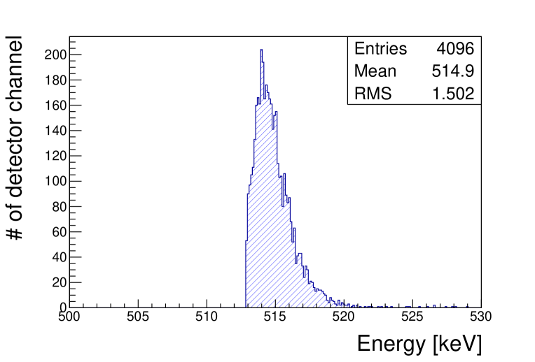
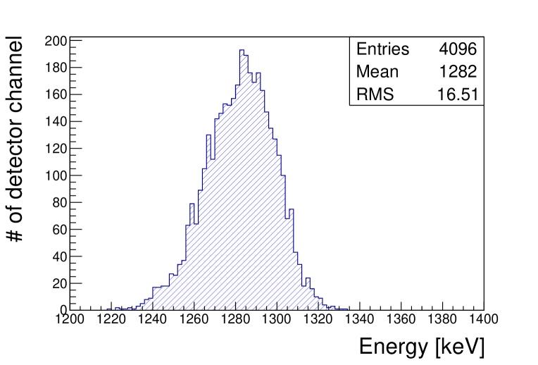
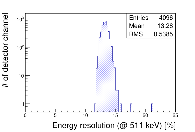
Finally, after the energy calibration has been applied, the energy
resolution for the 511 keV gamma is evaluated for all the
channels (Figure 26). Only one channel is out of the detector requirement: at least 20%
is necessary to effectively discriminate the 511 keV gammas from the
Compton events.
4.4 Coincidence Time Resolution
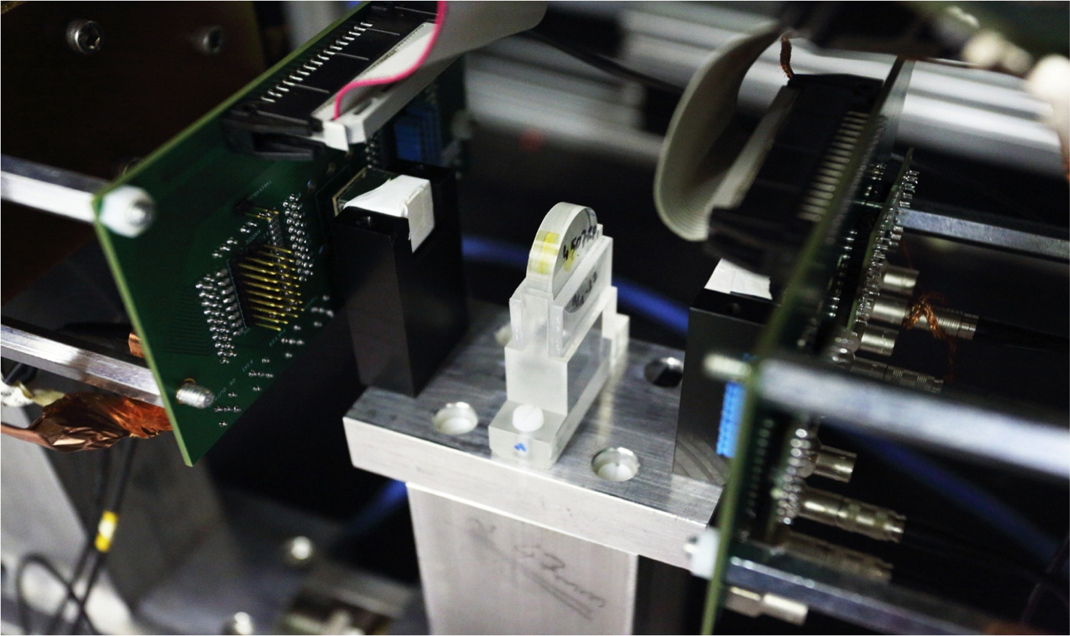
The coincidence time resolution of all the channels is measured using the setup shown in Figure 27.
The two modules are facing each other at 10 cm distance, while a 22Na point
like source is placed between them on the line connecting the module centers. One module has been selected as the reference for the measurement
of the other 256 modules.
The output signal of the SiPM is amplified and discriminated by NINO ASIC [16] and
sent to a high precision TDC (HPTDC- 25ps LSB) [17].
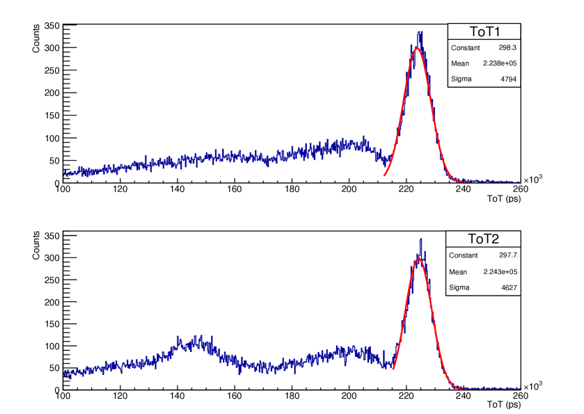
The data analysis is performed with a total number of 4x10⁶
triggers. As shown in Figure 28, the
Time-over-Threshold (ToT) spectra are obtained for any two channels in
coincidence; then a gaussian fit is applied to the peaks corresponding to
the 511 keV gamma events.
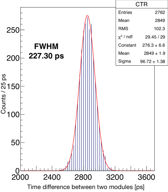
Hence the time difference for the gamma events of the
two channels are histogrammed and shown in Figure 29. A Gaussian
fit is applied and the FWHM is taken as the CTR of the channel
measured (227.3 ps 3.2 ps in this case).
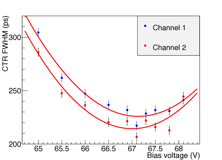
Figure 30 shows the CTR as a function of bias voltage
for two channels in coincidence with the reference module. Due to the increase of the SiPM Photon Detection
Efficiency (PDE) with the increase of excess bias, it is expected that
also the CTR improves accordingly. However, also the DCR increase with
the excess bias, and at a given point it becomes predominant.
In order to compare the CTR of all the 256 modules, an excess bias of 2.5 V is used
for any channel, the temperature is fixed at 19 oC and the NINO
ASIC threshold is kept fixed at
55 mV, which is equivalent to the threshold of 0.5 photoelectron.
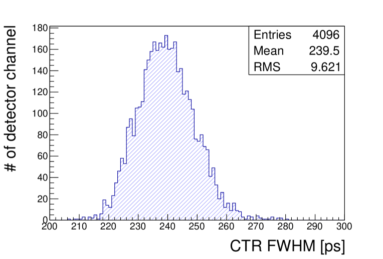
The CTR distribution for all the channels, measured with respect to
the reference module, is presented in
Figure 31 and shows an average of 239 10 ps FWHM.
5 Conclusions
In the frame of the EndoTOFPET-US project, all the detector modules
for the external plate have been characterized.
The gain, breakdown voltage, DCR and correlated noise have been
measured for all the received SiPMs, only 2% of them have been
rejected due to excess DCR.
The LYSO:Ce crystal matrices show a very good light yield and a
promising average CTR of 239 10 ps FWHM has been obtained, which
can be further improved in ideal conditions, such as lower
temperature or optimal excess bias for each channel. The average energy
resolution (at 511 keV) for all the modules is about 13%, and it complies with the minimum requirement of 20%. The light output
for every channel is available for a preliminary detector calibration, and
an average of about 1800 pixels fired for a 511 keV gamma
interaction has been obtained.
The detector modules are now ready for the integration with the
dedicated ASICs and the final mechanical assembly.
Acknowledgements
The research leading to these results has received funding from the European Union Seventh Framework Programme [FP7/2007-2013] under Grant Agreement no. 256984, and is supported by a Marie Curie Early Initial Training Network Fellowship of the European Community’s Seventh Framework Programme under contract number (PITN-GA-2011-289355-PicoSEC-MCNet).
References
- [1] Bar-Shalom et al., Clinical performance of PET/CT in evaluation of cancer: additional value for diagnostic imaging and patient management, J. Nucl. Med., (2003) 44:1200-1209.
- [2] P. Michl and T. Gress, Current Concepts and Novel Targets in Advanced Pancreatic Cancer, Gut. 2013;62(2):317-326.
- [3] R. Siegel et al., Cancer statistics, 2014, CA: A Cancer Journal for Clinicians 2014;64:9-29.
- [4] A. Sendler et al., Preoperative Evaluation of Pancreatic Masses with Positron Emission Tomography Using 18 F-fluorodeoxyglucose: Diagnostic Limitations, World J. Surg. 24, 1121-1129, 2000
- [5] H. Jadvar, Imaging evaluation of prostate cancer with 18 F-fluorodeoxyglucose PET/CT: utility and limitations, Eur J Nucl Med Mol Imaging (2013) 40 (Suppl 1):S5-S10
- [6] E. Garutti et al., EndoTOFPET-US a novel multimodal tool for endoscopy and Positron Emission Tomography, IEEE NSS/MIC Conf. Record (2012) 2096-2101. http://ieeexplore.ieee.org/xpl/articleDetails.jsp?arnumber=6551231
- [7] E. Roncali et al., Application of Silicon Photomultipliers to Positron Emission Tomography, Annals of Biomedical Engineering, (2011) Vol. 39, No. 4, pp. 1358-1377.
- [8] P. Buzhan et al., An advanced study of silicon photomultiplier, ICFA Instrum Bull. (2001) 23:28-42.
- [9] M.D Rolo et al., TOFPET ASIC for PET applications, JINST (2013) 8 C02050.
- [10] Wei Shen et al., STiC - A mixed Mode Chip for SiPM ToF Applications, IEEE NSS/MIC Conf. Record (2012) N14-37.
- [11] A. Tadday et al., Characterisation Studies of Silicon Photomultipliers , Nucl. Instrum. Meth. Phys. Res. A, (2010) 620 217.
- [12] G. Lutz, Semiconductor radiation detectors: device physics, Springer, (1999).
- [13] R. Pagano et al., Dark Current in Silicon Photomultiplier Pixels: Data and Model, IEEE transactions on electron devices, vol. 59, no. 9, pp. 2410–2416, Sept. 2012.
- [14] J. Trummer et al., Scintillation Properties of LuYAP and LYSO Crystals Measured with MiniACCOS, an Automatic Crystal Quality Control System, IEEE NSS/MIC Conf. Record (2005) 2807-2810.
- [15] Y. Shao, A new timing model for calculating the intrinsic timing resolution of a scintillator detector, Phys. Med. Biol. 52 (2007) 1103-1117.
- [16] F. Anghinolfi et al., NINO: An ultra-fast and low-power front-end amplifier/discriminator ASIC designed for the multigap resistive plate chamber, Nucl. Instrum. Meth. A 533 (2004) 183.
- [17] J.Christiansen, HPTDC, High Performance Time to Digital Converter version 2.2, CERN-EP/MIC (2004),