Epitaxial Growth of (1 1 1)-Oriented Spinel CoCr2O4/Al2O3 Heterostructures
Abstract
High quality (1 1 1)-oriented CoCr2O4/Al2O3 heterostructures were synthesized on the sapphire (0 0 0 1) single crystal substrates in a layer-by-layer mode. The structural properties are demonstrated by - reflection high energy electron diffraction, atomic force microscopy, X-ray reflectivity and X-ray diffraction. X-ray photoemission spectroscopy confirms that the films possess the proper chemical stoichiometry. This work offers a pathway to fabricating spinel type artificial quasi-two-dimensional frustrated lattices by means of geometrical engineering.
Recently, a great number of correlated complex heterostructures have been proposed to possess exotic quantum phenomena such as quantum Hall effectDi Xiao , topological insulatorRuegg ; Hu ; Kargarian ; A.Ruegg and quantum anomalous Hall effectWang . Among these artificial systems, there exists a common material design theme regarded as geometrical lattice engineering, namely growing a two dimensional “active material” sandwiched by wide band-gap insulators along the high index crystallographic [1 1 1] directions.A.Ruegg In such a way, the lattice geometries, electronic bandwidth, chemical environments and electron hopping routes of the materials are tuned to be tremendously different from the bulk. As a result, collective emergent quantum states are expected to emerge. Towards this goal, two main challenges hinder the fabrications of high quality (1 1 1) oriented heterostructures. First, the atomic layers along such direction are not charge neutral planes, the strong polarity mismatch between the film and the substrate may lead to the interfacial reconstruction, defect and impurity phase formationNakagawa ; Blok ; Sri_srp . Second, due to the limited availability of (1 1 1) oriented substrates, large lattice mismatch (5% and more) offen prevents forming flat and homogenious films. To date, most of the pioneering experimental efforts have focused on fabricating artificial perovskite (ABO3) type [1 1 1] superlatticesSri ; Gibert ; Herranz ; Sri_arkive due to the relatively simple lattice geometries. However there are few works published on the growth of other types of two dimensional correlated superlattices such as spinel type (AB2O4) which constitutes a family with rich and intriguing physical properties but crystallizes in a far more complex structure.Jak_nm
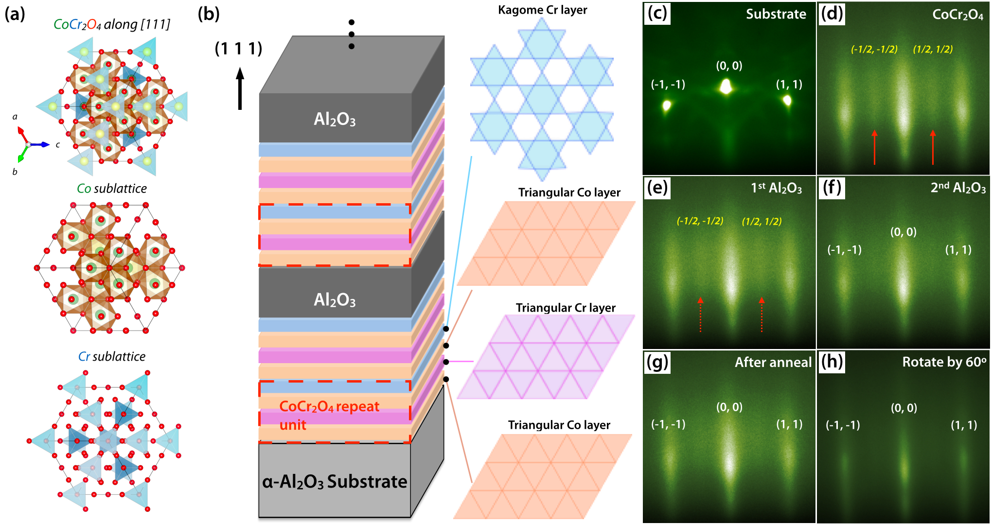
CoCr2O4 (CCO) has a prototypical normal spinel structure in which all the Co2+ ions are tetrahedrally coordinated by four oxygen ions and the Cr3+ ions are octahedrally coordinated by six oxygen ionsMenyuk [see Fig. 1 (a)]. This material exhibits several interesting physical phenomena including ferrimagnetismSingh , mutiferroicityYamasaki , and magnetic frustrationTomiyasu . The crystal structure of CCO viewed along the (1 1 1) orientation is composed of alternative ionic planes. The O sublattice has a dimension of 2.82 Å of the surface unit cell and presents a cubic close packing (CCP) arrangement of atoms in the form of ABCABC. The Co and Cr ionic planes between the O layers have three types of geometrically frustrated structures: triangular Co plane (T plane), triangular Cr plane (T’ plane) and kagomé Cr plane (K plane) as indicated in Fig. 1 (b). In the bulk 18 ionic planes form a full repeat pattern in the form of [O-K-O-T-T’-T]3 Vaz with the basic repeat unit [O-K-O-T-T’-T] as shown in Fig. 1 (b). In what follows this repeat unit is defined as “1CCO”.
In this Letter, we report on the fabrication of a new heterostructure CoCr2O4 (CCO)/Al2O3 (AlO) along the [1 1 1] direction. -AlO is selected as the spacer because its O sublattice consists of the hexagonal close packing (HCP) with a dimension of 2.74 Å, which is very close to that of CCO.Cousins ; Kirfel The compatibility of CCP and HCP lattices offers the perfect structural and chemical continuity between CCO and AlO layers, which effectively eliminates the polar and lattice mismatch issues. Good crystallinity and smooth surface morphology were demonstrated by - high pressure reflection-high-energy-electron-diffraction (RHEED) and atomic force microscopy (AFM). Synchrotron based X-ray diffraction (XRD) scan elucidated the growth direction of the heterostructures was along [1 1 1] with no impurity phases. Detailed film thickness of each layer and interfacial roughness were investigated by X-ray reflectivity (XRR). The chemical stoichiometry and core level electronic structures of CCO layer was investigated by monochromatic X-ray photoemission spectroscopy (XPS) indicating the oxidation states of Co to be 2+ and Cr to be 3+. The combined results allow to establish the high quality of the synthesized heterostructures with the quasi-two-dimensional frustrated kagomé and triangular layers.
A series of 2CCO/mAlO (m = 1 and 2 unit cells) superlattices was fabricated by the pulsed laser interval deposition methodKareev using a KrF excimer laser operating at 248 nm. The substrate was maintained at 800 ∘C under a partial pressure of 1 - 5 mTorr of oxygen during the deposition with the laser’s intensity 2 J/cm2 at the target. The ablation frequencies for CCO and AlO were 4 Hz and 2 Hz, respectively. Samples were annealed at the growth condition for 15 min and then cooled down to room temperature. The entire growth process was monitored by - RHEED with the incident electron beam along the [1 0 0] direction of the substrate. 1 m by 1 m AFM images were scanned over several different areas of the sample surface after the post anneal process to check the surface morphology and flatness. Detailed information about the thickness of each layer and interfacial roughness was obtained from the fittings of the X-ray reflectivity (Cu Kα1 line ( 1.5406 Å)) data. Synchrotron based X-ray diffraction measurement was performed at the beamline 6-ID-B of Argonne National Laboratory. The chemical valences and proper stoichiometry of the samples was investigated by core-level XPS measurements with monochromatic Al Kα source.
First we discuss the structural properties of the heterostructures. Fig. 1 (c)-(f) RHEED patterns present a detailed overlook of the deposition process. The clear specular and off-specular reflections on the zero-order Laue circle together with the Kikuchi lines in Fig. 1 (c) confirm a flat and good crystalline substrate surface. Once the CCO layer is formed on the substrate, two additional streaks occur in the middle of the specular and off-specular spots as shown in Fig. 1 (d). These half order reflections are the characteristic signature of spinel thin films grown on sapphire substrate and have also been observed in other works.Xiaoran ; Y.Gao ; Matzen The evolution of these RHEED images confirms that the epitaxial growth relation is CCO (1 1 1)[1 0] -AlO (0 0 0 1)[1 0 0]. When the first AlO is deposited onto the CCO layers, the typical spinel half orders can be still observed but become weaker [Fig. 1 (e)]. This is likely due to the formation of the -AlO phase which has an Al-deficient spinel structureSiqi . Since the -AlO has lower surface energyMcHale and more flexibility in cation distributionSiqi , it is likely to appear at the initial growth stage.Siqi ; Tanner As the second AlO layer is deposited, however, the half order streaks vanish and the RHEED pattern looks closer to the substrate pattern, as displayed in Fig. 1 (f). This observation indicates that the second AlO layer evolves into the -AlO phase. Further AlO deposition proudces the same RHEED patterns as Fig. 1 (f) which reveals the -AlO phase attains stability after the formation of the first transitional -AlO phase. The post-annealed RHEED images are shown in Fig. 1 (g). As seen, The distinct reflection streaks are maintained throughout the entire deposition implying the well developed crystallinity and the two dimensional layer-by-layer growth mode. To further examine the surface lattice symmetry, the samples were rotated by 60∘ steps relative to the original position. A characteristic RHEED image shown in Fig. 1 (h) reveal the same pattern, which confirms that the surface lattice has indeed a six-fold symmetry. In addition, the average rms surface roughness of the resultant samples is about 2 Å (not shown), which provides another strong evidence of the smooth surface morphology.
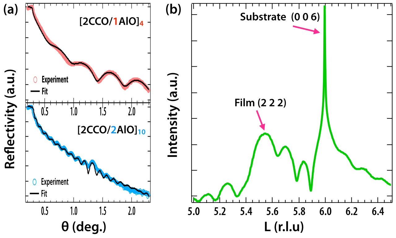
More detailed information about the thickness, the surface and interface roughness of these sets of superlattices was investigated by XRR. Two typical reflectivity curves with simulations for a thin sample [2CCO/1AlO]4 and a thick [2CCO/2AlO]10 sample are shown in Fig. 2 (a). The distinct intensity oscillations ( Kiessig fringes) over the whole scan range indicate abrupt interfaces and flat surface crystallinity of the samples. All of the fit parameters and the corresponding values are given in Table I. As seen, the fitted thickness of each layer is in excellent agreement with the values estimated from the specific number of laser pulses and RHEED oscillations of the reflected intensity. Furthermore, both superlattices maintain low roughness throughout the whole sample which corroborates the two-dimensional layer-by-layer stackings of each part also monitored by RHEED. The overall structural quality of the films have been investigated by synchrotron based XRD. The diffraction scan in the vicinity of sapphire (0 0 6) reflection on the [2CCO/1AlO]4 is shown in Fig. 2 (c). As seen, besides the sharp substrate (0 0 6) peak, the broad film peak surrounded by thickness fringes on both sides which correspond to the (2 2 2) reflection of the superlattice is also clearly observed. Based on the XRD data, good crystallinity and proper (1 1 1) orientation of the heterostructures has been confirmed.
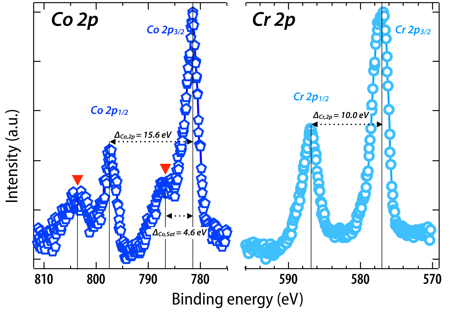
Next we turn our attention to the electronic properties of these samples. In order to investigate the valences and chemical stoichiometry of the sandwiched CCO layers, core-level XPS measurements were performed on the superlattices. Fig. 3 shows the core-level Co 2 and Cr 2 spectra collected on the representative 2CCO/1AlO sample. As seen on the left panel, the Co 2 spectrum consists of the spin-orbit split peaks corresponding to Co 23/2 and Co 21/2 at binding energies of 781.66 eV and 797.25 eV, respectively, and has an energy separation denoted as Co,2p 15.6 eV between them. The observed binding energy separation of 15.6 eV is characteristic for compounds containing Co2+ ions in a tetrahedral oxide environmentDillard ; Kumar . We also note that the binding energy separation in case of Co3+ containing compounds is usually smaller ( 15.1 eV) Okamoto .
In addition to the spin-orbit split main peaks, the Co 2 spectrum also consists of two intense shake-up satellite peaks located on the higher energy sides of the Co 23/2 and Co 21/2 peaks, which are highlighted by the red arrows. It is well knownOkamoto ; Bocquet that while Co2+ compounds show intense shake-up satellite peaks in Co 2 spectrum, the same features are much weaker in case of Co3+ containing compounds. In case of Co oxide samples, the shake-up satellite corresponds to the charge transfer excitation from a ligand oxygen 2 level to empty Co 3 states, and hence the relative energy separation from the shake-up satellite to its corresponding main peak is a distinct signature of the Co charge state. As seen in Fig. 3, the separation between the Co 23/2 peak and the corresponding shake-up satellite is 4.6 eV and is very close to that observed in other Co2+ compounds.Dillard On the right panel, the Cr 2 spectrum similarly consists of the spin-orbit split Cr 23/2 and Cr 21/2 peaks at the binding energies of 577.15 eV and 587.20 eV, respectively. The binding energy difference of 10.0 eV between the Cr 23/2 and Cr 21/2 peaks agrees very well with other Cr3+ containing compoundsKumar . Based on these XPS results, the valences of Co and Cr in our superlattice samples are assured to be 2+ and 3+, respectively.
In summary, we have fabricated artificial high quality (1 1 1)-oriented CCO/AlO superlattices with geometrically frustrated lattices on sapphire (0 0 0 1) substrate. The comprehensive structural and electronic characterizations established the layer-by-layer growth with proper chemical stoichiometry which consist of alternative stacking of kagomé and triangular atomic planes. Both the CCO and the AlO thickness can be digitally controlled. The presented results pave a way for fabricating unique two dimensional transition metal heterostructures on which a plethora of intriguing quantum phenomena can be expected.
The authors deeply acknowledges numerous fruitful discussions with D. Khomskii and G. Fiete. J.C. was supported by the DOD-ARO under Grant No. 0402-17291 and in part by the Gordon and Betty Moore Foundation. Work at the Advanced Photon Source, Argonne is supported by the U.S. DOE under Grant No. DEAC02 06CH11357.
References
- (1) D. Xiao, W. Zhu, Y. Ran, N. Nagaosa, and S. Okamoto, Nat. Commun. 2, 596 (2011).
- (2) A. Rüegg, and G. A. Fiete, Phys. Rev. B 84, 201103(R) (2011).
- (3) X. Hu, A. Rüegg, and G. A. Fiete, Phys. Rev. B 86, 235141 (2012).
- (4) M. Kargarian, A. Langair, and G. A. Fiete, Phys. Rev. B 86, 205124 (2012).
- (5) A. Rüegg, C. Mitra, A. A. Demkov, and G. A. Fiete, Phys. Rev. B 85, 245131 (2012).
- (6) Y. Wang, Z. Wang, Z. Fang, and X. Dai, arXiv: 1409.6797v1.
- (7) N. Nakagawa, H. Y. Hwang, and D. A. Muller, Nature Mater. 5, 204 (2006).
- (8) J. L. Blok, X. Wan, G. Koster, D. H. A. Blank, and G. Rijnders, Appl. Phys. Lett. 99, 151917 (2011).
- (9) S. Middey, P. Rivero, D. Meyers, M. Kareev, X. Liu, Y. Cao, J. W. Freeland, S. Barraza-Lopez, and J. Chakhalian, Sci. Rep. 4, 6819 (2014).
- (10) S. Middey, D. Meyers, M. Kareev, E. J. Moon, B. A. Gray, X. Liu, J. W. Freeland, and J. Chakhalian, Appl. Phys. Lett. 101, 261602 (2012).
- (11) M. Gibert, P. Zubko, R. Scherwitzl, J. Íñiguez, and J.-M. Triscone, Nature Mater. 11, 195 (2011).
- (12) G. Herranz, F. Sánchez, N. Dix, M. Scigaj, and J. Fontcuberta, Sci. Rep. 2, 758 (2012).
- (13) S. Middry, D. Meyers, D. Doennig, M. Kareev, X. Liu, Y. Cao, P. J. Ryan, R. Pentcheva, J. W. Freeland, and J. Chakhalian, arXiv: 1407.1570v2.
- (14) J. Chakhalian, A. J. Millis, and J. Rondinelli, Nature Mater. 11, 92 (2012).
- (15) N. Menyuk, K. Dwight, and A. Wold, J. Phys. 25, 528 (1964).
- (16) K. Singh, A. Maignan, C. Simon, and C. Martin, Appl. Phys. Lett. 99, 172903 (2011).
- (17) Y. Yamasaki, S. Miyasaka, Y. Kaneko, J. P. He, T. Arima, and Y. Tokura, Phys. Rev. Lett. 96, 207204 (2006).
- (18) K. Tomiyasu, J. Fukunaga, and H. Suzuki, Phys. Rev. B 70, 214434 (2004).
- (19) C.A.F. Vaz, V. E. Henrich, C. H. Ann, and E. I. Altman, J. Cryst. Growth 311, 2648 (2009).
- (20) C.S.G. Cousins, J. Phys. C Solid State Phys. 14, 1585 (1981).
- (21) A. Kirfel, and K. Eichhorn, Acta Cryst. A 46, 271 (1990).
- (22) M. Kareev, S. Prosandeev, B. Gray, J. Liu, P. Ryan, A. Kareev, E. J. Moon, and J. Chakhalian, J. Appl. Phys. 109, 114303 (2011).
- (23) X. Liu, M. Kareev, Y. Cao, J. Liu, S. Middey, D. Meyers, J. W. Freeland, and J. Chakhalian, Appl. Phys. Lett. 105, 042401 (2014).
- (24) Y. Gao, Y. J. Kim, S. A. Chambers, and G. Bai, J. Vac. Sci. Technol. A 15, 332 (1997).
- (25) S. Matzen, J.-B. Moussy, R. Mattana, K. Bouzehouane, C. Deranlot, F. Petroff, J. C. Cezar, M.-A. Arrio, P. Sainctavit, C. Gatel, B. Warot-Fonrose, and Y. Zheng, Phys. Rev. B 83, 184402 (2011).
- (26) S. Cao, A. J. Pedraza, D. H. Lowndes, and L. F. Allard, Appl. Phys. Lett. 65, 2940 (1994).
- (27) J. M. McHale, A. Auroux, A. J. Perrotta, and A. Navrotsky, Science 277, 788 (1997).
- (28) C. M. Tanner, M. Sawkar-Mathur, J. Lu, H.-O. Blom, M. F. Toney, and J. P. Chang, Appl. Phys. Lett. 90, 061916 (2007).
- (29) J. G. Dillard, C. V. Schenck, and M. H. Koppelman, Clays Clay Miner. 31, 69 (1983).
- (30) D. Kumar, P. Mohanty, V. P. Singh, J. K. Galivarapu, A. Banerjee, V. Ganesan, and C. Rath, Mater. Res. Bull. 54, 78 (2014).
- (31) Y. Okamoto, H. Nakano, T. Imanaka, and S. Teranishi, Bull. Chem. Soc. Jpn. 48, 1163 (1975).
- (32) A. E. Bocquet and A. Fujimori, J. Elec. Spec. Relat. Phenom. 82, 87 (1996).
| Sample | Items | Top AlO (Å) | Superlattice (Å) | Bottom CCO (Å) |
|---|---|---|---|---|
| thickness | 14.6 | 9.9/13.6 | 11.0 | |
| [2CCO/1AlO]4 | roughness | 3.5 | 2.6 | 1.0 |
| thickness | 30.8 | 9.8/27.0 | 12.9 | |
| [2CCO/2AlO]10 | roughness | 5.0 | 3.4 | 0.7 |