Full loss compensation in hybrid plasmonic waveguides under electrical pumping
Abstract
Surface plasmon polaritons (SPPs) give an opportunity to break the diffraction limit and design nanoscale optical components, however their practical implementation is hindered by high ohmic losses in a metal. Here, we propose a novel approach for efficient SPP amplification under electrical pumping in a deep-subwavelength metal-insulator-semiconductor waveguiding geometry and numerically demonstrate full compensation for the SPP propagation losses in the infrared at an exceptionally low pump current density of 0.8 kA/cm2. This value is an order of magnitude lower than in the previous studies owing to the thin insulator layer between a metal and a semiconductor, which allows injection of minority carriers and blocks majority carriers reducing the leakage current to nearly zero. The presented results provide insight into lossless SPP guiding and development of future high dense nanophotonic and optoelectronic circuits.
keywords:
Active plasmonics, surface plasmon amplification, metal-insulator-semiconductor structure, electrical pumpingUnknown University] Laboratory of Nanooptics and Plasmonics, Moscow Institute of Physics and Technology, 9 Institutsky Lane, 141707 Dolgoprudny, Russian Federation \abbreviationsSPP,MIS
1 Introduction
Surface plasmon polaritons (SPPs) being surface electromagnetic waves propagating along the interface between a metal and an insulator give a unique opportunity to overcome the conventional diffraction limit and thus can be used for light manipulation at the nanoscale 1. This gives plasmonic components a significant advantage over their photonic counterparts in the integration density and strength of light-matter interaction. However, high mode confinement is paid off by a significant localization of the SPP electromagnetic field in the metal and the resulting propagation length in nanoscale plasmonic waveguides does not exceed a few tens of micrometers due to absorption in the metal 1, 2, 3. Nevertheless, it is possible to overcome this limitation by compensating ohmic losses with optical gain in the adjacent dielectric. Full loss compensation was successfully demonstrated by optical pumping 4, 5, 6, which is easily implemented in a laboratory, but is impractical due to its very poor energy efficiency, stray illumination, and necessity of an external high power pump light source. In this regard, an efficient electrical pumping scheme is strongly needed for practical realization of SPP guides and circuits 7, 8, 9.
In this paper, we propose a novel SPP amplification scheme based on minority carrier injection in metal-insulator-semiconductor (MIS) structures and demonstrate numerically full loss compensation in an electrically pumped active hybrid plasmonic waveguide. In contrast to the techniques based on heterostructures and quantum wells 10, our approach gives a possibility to bring the active gain medium to the metal surface at a distance of a few nanometers. At the same time, a thin insulator layer can efficiently block the majority carrier current, which is quite high in metal-semiconductor Schottky-barrier-diode SPP amplifiers 11. This guarantees high mode confinement to the active region and very low threshold currents.
2 Operating principle
Realization of an electrical pumping scheme for loss compensation in SPP waveguides and cavities is a significant challenge, since there are at least two limitations in the development of plasmonic components. Firstly, plasmonics gives a possibility to reduce the mode size well below the diffraction limit, but, in order to use this opportunity, the component size should be comparable with the mode size. Accordingly, one has to use the SPP supporting metal-dielectric or metal-semiconductor interface as an electrical contact. Secondly, a limited choice of low-loss materials with negative real part of permittivity poses a serious challenge for efficient carrier injection, because gold, silver and copper typically form Schottky contacts to direct bandgap semiconductors. As a result, either the modal gain is rather low for full loss compensation, or the threshold current density is quite high 12, which leads to significant power consumption and low energy efficiency of the amplification scheme.
The proposed technique based on an electrically pumped MIS structure (Figure 1) is remarkably different from the established approaches 10, 13, 11, 14. First, SPP propagation losses are reduced by placing a very thin layer of a low refractive index insulator between the metal and semiconductor. In this case, the SPP electromagnetic field is pushed into the insulator reducing the portion of the SPP mode in the metal, which, however, does not impair the mode confinement 3. Second, and more important, a thin insulator layer can play a dual role: it is semi-transparent for electrons moving from the metal to semiconductor, which ensures favourable conditions for efficient minority carrier injection, and blocks the hole current. Such a unique feature gives a possibility to suppress high leakage currents 15, which are unavoidable in metal-semiconductor Schottky contacts 13, and not to form an ohmic contact to the semiconductor at the SPP supporting interface, as opposed to double-heterostructure and quantum-well SPP amplifiers 12. At the same time, the proposed scheme provides high density of non-equilibrium carriers right near the metal surface, at the distance equal to the thickness of the insulator layer. At a high bias voltage, it becomes possible to create a sufficiently high electron concentration in the semiconductor and to satisfy the condition for population inversion 16, which provides gain for the plasmonic mode propagating in the MIS waveguide.
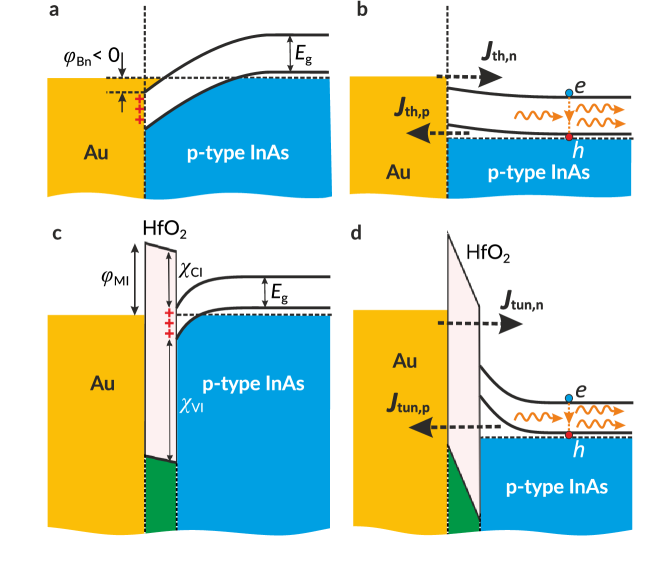
Previously, an attempt to describe the carrier transport in an electrically pumped hybrid plasmonic waveguide was made in Ref. 17. However, the authors assumed that both electrons and holes pass freely through the insulating layer and used the thermionic emission boundary conditions (literally the same as in the Schottky junction theory 18, 9). This is erroneous in the presence of the insulating barrier and contradicts the well-established theory of current transfer through thin insulating films 19, 20. In fact, the insulating barrier strongly suppresses the thermionic current, while the main current component is due to tunneling.
The electron and hole tunnel injection currents and across the MIS contact can be calculated by integrating the flux of carriers incident on the contact timed by the transparency of the insulating barrier (see Methods). According to the energy band diagram shown in Figure 1 c,d, the ratio of the electron tunneling probability to the hole tunneling probability can be easily estimated as
| (1) |
where is the valence band offset between the insulator and semiconductor, and is the barrier height for electrons at the metal-insulator interface. As evident from this simple expression, in order to block only one type of carriers, the effective barrier height for holes () must be substantially greater than that for electrons () or vice versa. Hafnium oxide appears to be a very promising material for electron injection into the p-type III-V materials thanks to the low tunneling mass 21 and large valence band and small conduction band offsets. Both theoretical 22 and experimental 23 studies report eV and eV for the HfO2/InAs interface. At the same time, eV for the gold contact 22, and the ratio equals five, which is high enough for practical applications.
We next explore the carrier transport in the semiconductor. It is important to note that the electric potential is abruptly screened near the interface between the insulator and heavily doped semiconductor, which directly follows from the solution of Poisson’s equation. At a doping density of cm-3, the estimated screening length is equal to 2 nm, while the electron mean free path limited by impurity scattering equals nm. This implies that electrons move ballistically through the screening region. Out of the screening region, the driving electric field is weak and the electron transport is governed by diffusion. Accordingly, the density distribution of the injected electrons is given by
| (2) |
where is the current density at the insulator-semiconductor interface, is the diffusion length, and is the equilibrium electron density. is the most critical parameter determining the distribution of carrier density in InAs, and, consequently, the material gain profile. It depends on the electron mobility through the electron diffusion coefficient and on the recombination rate through the electron lifetime . Equation (2) shows that, in order to compensate for the SPP propagation losses efficiently, should be comparable with the half of the SPP penetration depth in InAs (500 nm at m) or greater than the latter. The electron mobility in p-type InAs is mainly limited by charged impurity scattering and is about cm2V-1s-1 at 77 K at a doping level of cm-3 24. The main contributions to the carrier recombination in InAs at 77 K come from the nonradiative Auger process and radiative recombination due to spontaneous emission , where and are the equilibrium electron and hole densities, cm6/s are the Auger coefficients 25, and is the radiative recombination coefficient calculated to be cm3s-1. Since in a p-type semiconductor the density of electrons is much smaller than that of holes even at high injection levels, ps, which corresponds to a diffusion length of nm ensuring an excellent overlap between the distributions of the material gain (that is nearly proportional to the carrier concentration) and the SPP field.
The electron current at the semiconductor-insulator junction is mainly determined by quantum mechanical tunneling through the insulating layer. In the case of an ideal interface, is simply equal to the tunnel current . However, the presence of intrinsic and extrinsic surface states at the semiconductor-insulator interface has a significant impact on the characteristics of the tunnel MIS contact (see Methods). First, surface states act as charge storage centers and affect the voltage drop across the insulator layer and band bending in the semiconductor. Second, these states are recombination centers 25 and reduce the efficiency of electron injection. The electron current at the insulator-semiconductor interface is smaller than the tunnel injection current by the value of the surface recombination current . Third, direct tunneling from the metal to semiconductor through the surface states is also possible 26, 27. This process contributes only to the majority carrier current and reduces the energy efficiency of the SPP amplification scheme. Fortunately, intrinsic surface states in InAs have a moderate density cm-2eV-1 28. Deposition of metal 29 or insulator 30 layers produces additional defects and can be increased up to cm-2eV-1 at HfO2/InAs interfaces 31. Nevertheless, both intrinsic and extrinsic states can be treated by surface passivation before HfO2 deposition. The reported values of at the trimethylaluminum-treated HfO2/InAs interface is about cm-2eV-1 32, while advanced oxygen-termination and surface reconstruction techniques give a possibility to reduce down to cm-2eV-1 33, which eliminates the influence of surface states on carrier transport in high quality samples.
3 Active hybrid plasmonic waveguide in the passive regime
In order to achieve strong SPP mode localization and efficiently inject both electrons and holes into the active semiconductor region, a modified T-shaped plasmonic waveguide approach 11 has been implemented [Figure 2 (a)]. InAs rib with an acceptor concentration of cm-3 on InAs substrate is covered by a thin HfO2 layer and surrounded by a low refractive index dielectric (SiO2) to confine optical modes in the lateral direction. Finally, a metal layer is placed on top of the semiconductor-insulator structure to form an SPP supporting interface and a tunnel MIS contact for electron injection, while the substrate plays a role of the ohmic contact for majority carrier (hole) injection.
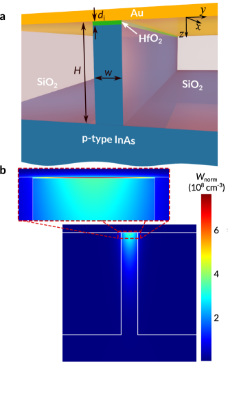
Two-dimensional eigenmode simulations using the finite element method reveal that the waveguide depicted in Figure 2(a) supports a deep-subwavelength TM00 SPP mode [Figure 2(b)]. For the chosen waveguide dimensions, at a free space wavelength of 3.22 m, which appears to be optimal for SPP amplification (see Section 4 for details), the effective index of the TM00 mode is equal to 2.799 and the propagation length in the passive regime assuming the semiconductor to be lossless is about 66 m corresponding to a modal loss of cm-1. The other modes supported by the T-shaped waveguide are very leaky photonic modes. In spite of poor field confinement to the lossy metal, propagation lengths of the photonic TM10, TE00, and TE10 modes are 5.8 m, 12.8 m and 2.7 m, respectively, which are much shorter than that of the TM00 mode due to leakage into the high refractive index substrate. The rib height of m is close to the optimum, since, as decreases, the radiation loss of the plasmonic mode becomes substantially greater than the absorption in the metal and the SPP propagation length decreases down to 39 m at m. On the other hand, greater rib heights do not provide a significant loss reduction, while high-aspect-ratio structures are difficult in fabrication. For the selected optimal geometrical parameters, the SPP mode demonstrates an exceptionally high level of confinement 37 within the InAs region of more than 95% provided by the small mode width and high group index.
4 Full loss compensation in a deep-subwavelength waveguide
Applying a negative voltage to the top Au electrode of the active plasmonic waveguide shown in Figure 2a, one injects electrons into the p-type InAs region. This creates a high density of non-equilibrium electrons in the semiconductor rib, which reduces absorption in InAs 16. As the bias voltage increases, the quasi-Fermi level for electrons shifts upward towards the conduction band. When the energy difference between quasi-Fermi levels for electrons and holes exceeds the energy of the SPP quantum, InAs starts to compensate for the SPP propagation losses. The modal gain is given by the overlap integral of the material gain profile and the electric field distribution of the SPP mode:
| (3) |
Here, and are the complex amplitudes of the electric field and the local power density of the SPP mode, respectively, and is attributed to the SPP radiation and ohmic losses (see Section 3). In turn, the material gain coefficient is related to the carrier quasi-Fermi levels and by the integral over transitions between the energy levels in the conduction and valence bands separated by the energy (see Methods). In heavily doped semiconductors, the material gain strongly depends on the impurity concentration 38, so are the electrical properties (, , and ). The optimal acceptor concentration is found to be cm-3. As the doping concentration increases, the Auger recombination rate and the impurity scattering rate rapidly increase greatly reducing the electron diffusion length. On the other hand, at lower doping levels, the number of free electron states in the valence band is insufficient to provide a pronounced gain upon electrical injection. At the given impurity concentration and a reasonably high density of injected electrons of cm-3 (which corresponds to ), the material gain spectrum exhibits a maximum of 310 cm-1 at eV ( m), sufficiently high for the net SPP amplification.
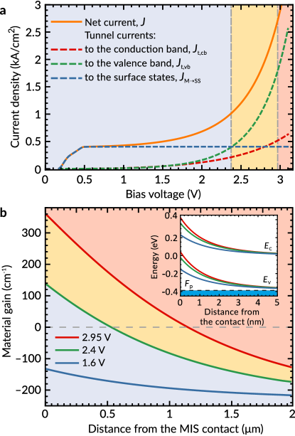
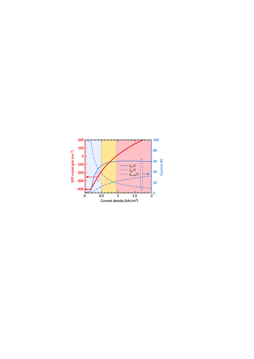
Figure 3 shows the simulated gain-current characteristic of the plasmonic TM00 mode in the active hybrid plasmonic waveguide for the HfO2/InAs interfaces of different quality. All curves exhibit the same trend. At zero bias, the concentration of holes in the semiconductor is many orders of magnitude greater than that of electrons, InAs strongly absorbs the SPP propagating in the waveguide and the modal loss is two-and-a-half times greater than in the case of the lossless (e.g. wide bandgap) semiconductor. As the bias voltage increases, electrons are injected in the InAs rib (Figure 4a), which reduces absorption in the semiconductor near the MIS contact, but still, InAs strongly absorbs at a distance greater than (Figure 4b). Nevertheless, the SPP modal loss steadily decreases with the injection current (this region is shown in blue in Figure 3). At some point (green curve in Figure 4b), the overlap between the distributions of the material gain and the SPP field is zero and, at higher bias voltages, the gain in InAs produced by injected electrons partially compensates for the SPP propagation losses.
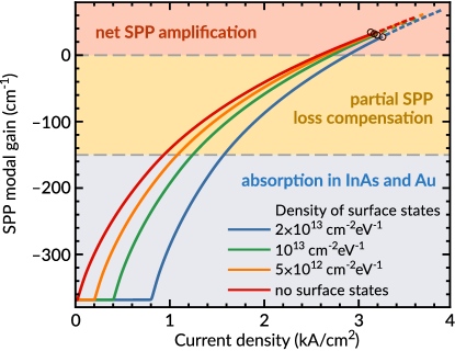
Eventually, at an injection current of about 2.7 kA/cm2 (Figure 3), ohmic losses and radiation losses of the plasmonic mode are fully compensated. For comparison, previously, net SPP amplification was reported at current densities of the order of 20 kA/cm2 in waveguide structures based on the Au/p-InAs Schottky contact 11. Here, we have achieved one order of magnitude reduction in the threshold current density using the tunneling Au/HfO2/InAs contact instead of the Schottky contact and blocking the majority carrier current with a thin insulator layer.
As evident from Figure 3, the current density required for full loss compensation is robust against the quality of the HfO2/InAs interface. It is equal to 2.6 kA/cm2 in the case of the ideal interface and increases by only 12% as the density of surface states increases to cm-2eV-1. This small increase is completely attributed to the tunnel current from the metal to surface states (Figure 4a), while the surface recombination current is more than six orders of magnitude lower than the total current. This is explained by the energy barrier for electrons in the semiconductor due to band bending at the HfO2/InAs interface under high forward bias (see inset in Figure 4b) 40.
Interesting is the possibility to control optical and electrical properties of the active T-shaped hybrid plasmonic waveguide by varying the thickness of the insulator layer. As increases, the portion of the SPP field in the metal decreases, which results in a decrease of ohmic losses. At the same time, thicker insulating layers block the majority carrier current more efficiently as follows from Equation (1). However, it appears that the tunnel current is very sensitive to the thickness of the HfO2 layer and nm is the optimal value. As is decreased by 0.5 nm (one atomic layer), the majority carrier current drastically increases due to direct tunneling from the metal to surface states and, at a surface-state density of cm-2eV-1, the SPP propagation losses are fully compensated at a very high current density of 7.5 kA/cm2 . On the other hand, the 3.5 nm thick HfO2 layer efficiently blocks the majority current, but the barrier width for minority carriers is also increased and higher bias voltage are needed for efficient electron injection. As a result, the electric field in HfO2 rapidly reaches the breakdown value of 1 V/nm 39 as the electron current increases. The minimum achievable SPP modal loss is 240 cm-1 that is much greater than cm-1 evaluated in the case of the lossless (e.g. wide bandgap) semiconductor. For the optimal HfO2 layer thickness of 3 nm, the breakdown condition V corresponds to the net SPP modal gain of 40 cm-1, which can be increased up to 160 cm-1 in high-quality samples, where the breakdown electric field can be as high as 1.2 V/nm 39.
5 Low-current loss compensation in copper waveguide
The effective density of states in the valence band of InAs is 75 times greater than in the conduction band. Therefore, in spite of the relatively large ratio for the Au/HfO2/InAs contact, the electron tunnel current does not exceed that of holes (Figure 4a). In addition, under high forward bias, the effective barrier height for holes, which can be estimated as the energy difference between the hole quasi-Fermi level in InAs near the insulator-semiconductor contact and the valence band edge of HfO2 at , is substantially reduced due to band bending (inset in Figure 4b) and the ratio rapidly decreases as the bias voltage increases (Figure 4a). To improve the efficiency of the amplification scheme, one should increases the difference between barrier heights and as it can be seen from equation (1). To satisfy this demand, one or more materials in the T-shaped active plasmonic waveguide (Figure 2a) should be replaced.
It would be naive to expect better characteristics in plasmonic structures based on metals different from gold and silver, however, in electrically pumped active plasmonic waveguides, both electrical and optical processes are involved, and the optimal configuration is typically the result of the interplay between them. Copper is characterized by higher absorption at optical frequencies than gold 41, 42 and the modal loss of the plasmonic TM00 mode in the T-shaped waveguide increases from 152 cm-1 to 189 cm-1. On the other hand, the electron work function of copper is equal to 4.7 eV, which is 0.4 eV lower than that of gold. Such a small difference is sufficient to produce an appreciable effect on carrier tunneling through the insulating barrier and increase the efficiency of minority carrier injection in InAs. The electron-to-hole transparency ratio of the Au/HfO2/InAs contact is as large as 20, and the electron tunnel current substantially exceeds the hole tunnel current (Figure 5).
At a surface-state density of cm-2eV-1, the propagation losses of the plasmonic mode are fully compensated at a current density of 0.95 kA/cm2, which is significantly smaller than in the case of the gold active plasmonic waveguide despite higher absorption losses of the SPP mode. Passivation of the InAs surface reduces the density of surface states by orders of magnitude 33, and the regime of full loss compensation is reached at a very low current kA/cm2, which is comparable with the threshold currents in double-heterostructure InAs lasers 43. In addition, the copper waveguide operates at smaller bias voltages than the gold one. First, this results in lower energy consumption per unit waveguide length, which decreases from 30 mW/mm to 8.2 mW/mm in the regime of full loss compensation. Second, and more importantly, smaller bias voltages create lower electric fields in the HfO2 layer. The breakdown condition ( V/nm) corresponds to the net SPP modal gain of 220 cm-1 that is much higher than in the similar gold waveguide. This allows one to use the proposed amplification scheme in nanolasers 44, where not only ohmic, but also high radiation losses have to be compensated.
6 Conclusion
In summary, we have proposed a novel approach for SPP amplification in deep-subwavelength structures under electrical pumping and demonstrated full loss compensation in an active hybrid plasmonic waveguide. The amplification scheme is based on efficient minority carrier injection in metal-insulator-semiconductor contacts at large forward bias, which creates a population inversion in the semiconductor and provides optical gain for the plasmonic mode propagating along the metal interface. At the same time, a thin insulator layer blocks majority carriers giving a possibility to reduce the leakage current to that in double-heterostructure lasers. Comprehensive electronic/photonic simulations show that the SPP propagation losses can be fully compensated in the electrically driven active hybrid plasmonic waveguide based on the Au/HfO2/InAs structure at a current density of only 2.6 kA/cm2. Moreover, by replacing gold with copper, one significantly improves the efficiency of minority carrier injection, and, in spite of higher ohmic losses, the current density in the regime of lossless SPP propagation is reduced down to 0.8 kA/cm2. Such an exceptionally low value demonstrates the potential of electrically pumped active plasmonic waveguides and plasmonic nanolasers for future high-density photonic integrated circuits.
7 Methods
Evaluation of the tunnel current. Tunnel current density across the MIS contact is given by 19
| (4) |
Here, the subscript indicates either the conduction (cb) or valence (vb) band, , , and are the Fermi-Dirac electron distribution functions in the metal and respective semiconductor bands, is the maximum transverse momentum of the electron in the semiconductor at a given energy , is the probability of carrier tunneling to the -th band, is the conduction band edge in the semiconductor, is the Planck s constant and is the elementary charge.
The tunneling probability is obtained in the WKB-approximation
| (5) |
where is the conduction band edge [] or the valence band edge [] of the insulator, is the effective electron mass in the insulator (tunneling mass), and is its thickness.
Accounting for the surface states at the HfO2/InAs interface. The surface charge and spurious currents associated with surface states can be found from the detailed balance between three major processes
(1) electron capture from the conduction band of the semiconductor to the surface states and their thermal emission to the band;
(2) hole capture and thermal emission;
(3) direct tunnelling from the metal to surface states.
Following Landsberg and Klimpke 45, we obtain the occupancy of the surface state with energy in a steady state:
| (6) |
In the above expression, we have introduced the rates , , and characterizing the abovementioned population and depopulation processes; and are the electron and hole capture cross sections, and are the electron and hole thermal velocities, and is the rate of direct tunnel transitions from the metal to surface states . The latter can be expressed as 27, where is the barrier transparency evaluated at zero transverse momentum, and fs is the characteristic electron escape time from the surface state to the metal. Experimental studies reveal the donor-type behavior of surface defects in InAs 30. In the neutral state, their hole capture cross-section is about cm-2 25, while, in the charged state, the electron capture cross-section sn is estimated to be cm-2 using the theory of electron capture mediated by cascade phonon emission 46. Such a small cross-section is attributed to the slow phonon emission rate, which is inseparably linked with the high electron mobility of cm2V-1s-1 in intrinsic InAs 47.
Assuming the density of surface states per unit area per unit energy to be uniform over the band gap, one can write expressions for the surface charge density
| (7) |
the current density associated with surface recombination
| (8) |
and the direct tunneling current from the metal to the surface states
| (9) |
Finally, equations (2), (4), (7), (8), and (9) are solved with Poisson’s equation .
Calculation of the material gain. Optical gain in the semiconductor is obtained by integrating the transition probabilities between electron states in the conduction and valence bands over the states’ energies:
| (10) |
Here, and are the densities of states in the conduction and valence bands of the semiconductor, respectively, and are the Fermi-Dirac distribution functions for the conduction and valence bands, is the average matrix element connecting Bloch states near the band edge 48, and is the envelope matrix element calculated using Stern’s model 38. In heavily doped semiconductors, , , and consequently the material gain, strongly depend on the impurity concentration, while at low doping levels is strongly peaked at the energy corresponding to the exact momentum conservation for the electron-photon system 16, 38, and equation (10) is reduced to the that in the band-to-band transition model with the -selection rule.
This work was supported by the Russian Science Foundation (grant no. 14-19-01788).
References
- 1 Kriesch, A.; Burgos, S.P.; Ploss, D.; Pfeifer, H.; Atwater, H.A.; Peschel, U. Functional Plasmonic Nanocircuits with Low Insertion and Propagation Losses. Nano Lett. 2013, 13, 4539-4545.
- 2 Conway, J.A.; Sahni, S.; Szkopek, T. Plasmonic interconnects versus conventional interconnects: a comparison of latency, crosstalk and energy costs. Opt. Express 2007, 15, 4474-4484.
- 3 Sorger, V.J.; Ye, Z.; Oulton, R.F.; Wang, Y.; Bartal, G.; Yin, X.; Zhang, X. Experimental demonstration of low-loss optical waveguiding at deep sub-wavelength scales. Nat. Comm. 2011, 2, 331.
- 4 Kena-Cohen, S.; Stavrinou, P.N.; Bradley, D.D.; Maier, S.A. Confined Surface Plasmon-Polariton Amplifiers. Nano Lett. 2013, 13, 1323-1329.
- 5 Oulton, R.F.; Sorger, V.J.; Zentgraf, T.; Ma, R.M.; Gladden, C.; Dai, L.; Bartal, G.; Zhang, X. Plasmon lasers at deep subwavelength scale. Nature 2009, 461, 629-632.
- 6 Flynn, R.A.; Kim, C.S.; Vurgaftman, I.; Kim, M.; Meyer, J.R.; Mäkinen, A.J., Bussmann, K.; Cheng, L.; Choa, F.-S.; Long, J.P. A room-temperature semiconductor spaser operating near 1.5 m. Opt. Express 2011, 9, 8954-8961.
- 7 Fang, A.W.; Jones, R.; Park, H.; Cohen, O.; Raday, O.; Paniccia, M.J.; Bowers, J.E. Integrated AlGaInAs-silicon evanescent racetrack laser and photodetector. Opt. Express 2007, 15, 2315-2322.
- 8 Fedyanin, D.Yu.; Arsenin, A.V. Semiconductor Surface Plasmon Amplifier Based on a Schottky Barrier Diode. AIP Conf. Proc. 2010, 1291, 112-114.
- 9 Fedyanin, D.Yu.; Arsenin, A.V. Surface plasmon polariton amplification in metal-semiconductor structures. Opt. Express 2011, 19, 12524-12531.
- 10 Costantini, D.; Bousseksou, A.; Fevrier, M.; Dagens, B.; Colombelli, R. Loss and Gain Measurements of Tensile-Strained Quantum Well Diode Lasers for Plasmonic Devices at Telecom Wavelengths. IEEE J. Quantum Electron. 2012, 48(1), 73-78.
- 11 Fedyanin, D.Yu.; Krasavin, A.V.; Arsenin, A.V.; Zayats, A.V. Surface Plasmon Polariton Amplification upon Electrical Injection in Highly Integrated Plasmonic Circuits. Nano Lett. 2012, 12, 2459-2463.
- 12 Costantini, D. Compact generation and amplification of surface plasmon polaritons at telecom wavelengths. PhD thesis, University Paris Sud, Paris XI, 2013.
- 13 Fedyanin, D.Yu. Toward an electrically pumped spaser. Opt. Letters 2012, 37, 404-406.
- 14 Hill, M.T.; et al., Lasing in MIM sub-wavelength plasmonic waveguides. Opt. Express 2009, 17, 11107-11112.
- 15 Wade, G.; Wheeler, C.A.; Hunsperger, R.G. Inherent properties of a tunnel-injection laser. Proceedings of the IEEE 1965, 53, 98-99.
- 16 Casey, H.C.; Panish, M.B. Heterostructure Lasers. Part A. Fundamental Principles; Academic Press, New York, 1978.
- 17 Wijesinghe, T.; Premaratne, M.; Agrawal, G.P. Electrically pumped hybrid plasmonic waveguide. Opt. Express 2014, 22, 2681-2694. The results obtained in this reference assume free passage of carriers through the barrier layer with injection velocity equal to the thermal velocity. This contradicts to the established theories of transport in MIS structures 20, 19 and leads to an overestimate of injection current and, hence, SPP gain. Due to high potential barrier in metal/insulator interface, the thermionic injection cannot be actually efficient, while the dominating transport mechanism is due to tunneling.
- 18 Green, M.A.; Shewchun, J. Minority carrier effects upon the small signal and steady-state properties of Schottky diodes. Solid-State Electron. 1973, 16, 1141-1150.
- 19 Stratton, R. Volt-current characteristics for tunneling through insulating films. J. Phys. Chem. Solids 1962, 23, 1177-1190.
- 20 Card, H.C.; Rhoderick, E.H. Studies of tunnel MOS diodes I. Interface effects in silicon Schottky diodes. J. Phys. D: Appl. Phys. 1971, 4, 1589.
- 21 Chang, Y.C.; Huang, M.L.; Lee, K.Y.; Lee, Y.J.; Lin, T.D.; Hong, M.; Kwo, J.; Lay, T.S.; Liao, C.C.; Cheng K.Y. Atomic-layer-deposited HfO2 on In0.53Ga0.47As: Passivation and energy-band parameters. Appl. Phys. Lett. 2008, 92, 072901.
- 22 Robertson, J.; Falabretti, B. Band offsets of high-k gate oxides on III-V semiconductors. J. Appl. Phys. 2006, 100, 014111.
- 23 Wheeler, D.C. High-k InAs metal-oxide-semiconductor capacitors formed by atomic layer deposition. PhD thesis, University of Notre Dame, Notre Dame, Indiana, 2009.
- 24 Sze, S.M. Physics of semiconductor devices, Chapter 1.5.1; John Wiley & Sons, New York, 1981.
- 25 Abakumov, V.N.; Perel, V.I.; Yassievich, I.N. Nonradiative Recombination in Semiconductors; North-Holland, 1991.
- 26 Card, H.C. On the direct currents through interface states in metal-semiconductor contacts. Solid-State Electron. 1975, 18, 881-883.
- 27 Lundström, I.; Svensson, C. Tunneling to traps in insulators. J. Appl. Phys. 1972, 43, 5045-5047.
- 28 Noguchi, M.; Hirakawa, K.; Ikoma, T. Intrinsic electron accumulation layers on reconstructed clean InAs (100) surfaces. Phys. Rev. Lett. 1991, 66, 2243.
- 29 Betti, M.G.; Bertoni, G.; Corradini, V.; De Renzi, V.; Mariani, C. Metal-induced gap states at InAs (110) surface. Surf. Sci. 2000, 454, 539-542.
- 30 Mönch, W. Semiconductor surfaces and interfaces, Springer, 2001; Vol. 26.
- 31 Wheeler, D.; Wernersson, L.-E.; Fröberg, L.; Thelander, C.; Mikkelsen, A.; Weststrate, K.-J.; Sonnet, A.; Vogel, E.M.; Seabaugh, A. Deposition of HfO2 on InAs by atomic-layer deposition. Microelectronic Engineering 2009, 86, 1561-1563.
- 32 Wang, C.H.; Doornbos, G.; Astromskas, G.; Vellianitis, G.; Oxland, R.; Holland, M.C.; Huang, M.L.; Lin, C.H.; Hsieh, C.H.; Chang, Y.S.; Lee, T.L.; Chen, Y.Y.; Ramvall, P.; Lind, E.; Hsu, W.C.; Wernersson, L.-E.; Droopad, R.; Passlack, M.; Diaz, C.H. High-k dielectrics on (100) and (110) n-InAs: Physical and electrical characterizations. AIP Advances 2014, 4, 047108.
- 33 Wang, C.H.; Wang, S.W.; Doornbos, G.; Astromskas, G.; Bhuwalka, K.; Contreras-Guerrero, R.; Edirisooriya, M.; Rojas-Ramirez, J.S.; Vellianitis, G.; Oxland, R.; Holland, M.C.; Hsieh, C.H.; Ramvall, P.; Lind, E.; Hsu, W.C.; Wernersson, L.-E.; Droopad, R.; Passlack, M.; Diaz, C.H. InAs hole inversion and bandgap interface state density of cm2eV-1 at HfO2/InAs interfaces. Appl. Phys. Lett. 2013, 103, 143510.
- 34 Malitson, I.H. Interspecimen Comparison of the Refractive Index of Fused Silica. J. Opt. Soc. Am. 1965, 55, 1205-1208.
- 35 Bright, T.J.; Watjen, J.I.; Zhang, Z.M.; Muratore, C.; Voevodin, A.A. Optical properties of HfO2 thin films deposited by magnetron sputtering: From the visible to the far-infrared. Thin Solid Films 2012, 520, 6793-6802.
- 36 Tsou, Y.; Ichii, A.; Garmire, E.M. Improving InAs double heterostructure lasers with better confinement. IEEE J. Quantum Electron. 1992, 28, 1261-1268.
- 37 Robinson, J.T.; Preston, K.; Painter, O.; Lipson, M. First-principle derivation of gain in high-index-contrast waveguides. Opt. Express 2008, 16, 16659-16669.
- 38 Casey H.C., Stern, F. Concentration-dependent absorption and spontaneous emission of heavily doped GaAs. J. Appl. Phys. 1976, 47, 631-643.
- 39 Chang, C; Hwu, J.-G. Characteristics and reliability of hafnium oxide dielectric stacks with room temperature grown interfacial anodic oxide. IEEE Transactions on Device and Materials Reliability 2009, 9, 215-219.
- 40 Rimmer, J.S.; Langer, J.M.; Missous, M.; Evans, J.H.; Poole, I.; Peaker, A.R.; Singer, K.E. Minority-carrier confinement by doping barriers. Materials Science and Engineering: B 1991, 9, 375-378.
- 41 Ordal, M.A.; Long, L.L.; Bell, R.J.; Bell, S.E.; Bell, R.R.; Alexander Jr., R.W.; Ward C.A. Optical properties of the metals Al, Co, Cu, Au, Fe, Pb, Ni, Pd, Pt, Ag, Ti, and W in the infrared and far infrared, Applied Optics 1983, 22, 1099-1119.
- 42 Lenham, A.P.; Treherne, D.M. Applicability of the Anomalous Skin-Effect Theory to the Optical Constants of Cu, Ag, and Au in the Infrared. J. Opt. Soc. Am. 1966, 56, 683-685.
- 43 Aydaraliev, M.; Zotova, N.V.; Karandashov, S.A.; Matveev, B.A.; Stus’, N.M; Talalakin, G.N. Low-threshold long-wave lasers ( m) based on III-V alloys. Semicond. Sci. Technol. 1993, 8, 1575.
- 44 Stockman, M.I. Nanoplasmonics: past, present, and glimpse into future. Opt. Express 2011, 19, 22029-22106.
- 45 Landsberg, P.T.; Klimpke, C.M. Surface recombination effects in an improved theory of a p-type MIS solar cell. Solid-State Electron. 1980, 23, 1139-1145.
- 46 Abakumov, V.N.; Iassievich, I.N. Cross section for the recombination of an electron on a positively charged center in a semiconductor. Sov. Phys. JETP 1976, 71, 657-664.
- 47 Adachi, S. Properties of Group-IV, III-V and II-VI Semiconductors; John Wiley & Sons, New York, 2005.
- 48 Coldren, L.A.; Corzine, S.W.; Mashanovitch, M.L. Diode lasers and photonic integrated circuits, John Wiley & Sons, New York, 2012.