Aharonov Bohm effect in 2D topological insulator.
Abstract
We present magnetotransport measurements in HgTe quantum well with inverted band structure, which expected to be a two-dimensional topological insulator having the bulk gap with helical gapless states at the edge. The negative magnetoresistance is observed in the local and nonlocal resistance configuration followed by the periodic oscillations damping with magnetic field. We attribute such behaviour to Aharonov-Bohm effect due to magnetic flux through the charge carrier puddles coupled to the helical edge states. The characteristic size of these puddles is about 100 nm.
pacs:
73.63.-b, 73.23.-b, 85.75.-dI Introduction
The investigation of the quantum interference phenomena, such as Aharonov-Bohm (AB) oscillations and weak localizations, provides an important information about fundamental properties of various electronic systems lee . Recently new class of materials with interesting properties have emerged, called topological insulators (TI), which are insulating in the bulk and characterized by the existence of robust gapless excitations at their surface hasan ; qi ; moore ; moore2 . Manifestation of AB oscillations in topological insulators, can be utilized to probe the surface nature in TI and its properties. The time-reversal-symmetric 2D topological insulator is induced by a strong spin-orbit interaction kane ; bernevig ; maciejko1 ; yang ; chang1 and characterized by edge modes with opposite spins propagating in opposite directions. The 2D TI have been realized in HgTe quantum wells with inverted band structure konig ; buhmann . Aharonov Bohm oscillations is intimately related to the weak localization (WL) corrections. For example, WL phenomena is discussed in terms of the collective action of the magnetic flux through the random loops of the pair of time reversed trajectories lee . The constructive interference of these path in return point is suppressed by AB flux, which lead to the resistance increase and negative magnetoresistance altshuler . The spin orbit coupling strongly modifies the quantum corrections the conductivity, it leads to a destructive interference between clockwise and counter-clockwise trajectories and changes the WL to weak anti-localization behavior (WAL).
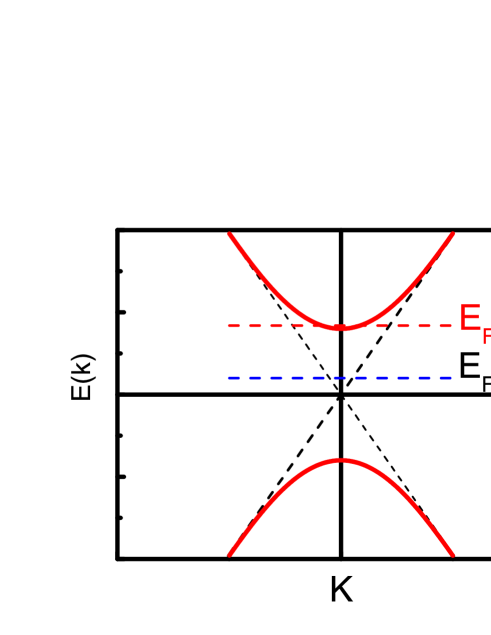
In 2D topological system WL is quite different from conventional 2D metals and strongly affected by the Dirac spectrum of massive fermions ostrovsky ; tkachov with the mass proportional to the band gap. The electronic spectrum is shown in Figure 1. The band structure has a simple parabolic form near the bottom of the band (marked by in Figure 1 and linear Dirac-like dispersion relation at high Fermi energy . When the Fermi energy lies in the bulk gap near the charge neutrality point (CNP), spectrum described by pair of the helical edge states (Figure 1). More over, the edge state must have linear Dirac like dispersion. The localization corrections are strongly governed by such remarkable property of the spectrum. When the Fermi energy is small, the effective spin-orbit coupling is weak, and one can expect the conventional WL behaviour ostrovsky . When the Fermi energy becomes larger than the gap width, the energy dispersion is linear, and theory describes crossover from WL to WAL behaviour ostrovsky ; tkachov ; tkachov2 ; ostrovsky2 . The magnetoresistance of 2D TI with a dominant edge state contribution is described by two mechanisms: first scenario relies to the frequent deviations of the edge electrons into the disordered AB flux threaded 2D bulk maciejko ; and second scenario to the localization of the helical edge sates due to the collective action of the random magnetic flux through the loops, naturally formed by rough edges of the sample deplace . Both models predict quasi-linear positive magnetoresistance MR. According to this theoretical predictions positive MR was observed in 8 nm HgTe quantum wells gusev2 .
Recently interaction of the helical states with multiple puddles of charge carriers formed by fluctuations in the donor density has been considered in 2D topological insulators vayrynen . This leads to significant inelastic backscattering due to the dwelling of carriers in the puddles and to a large resistance, which depends weakly on temperature. Moreover, carriers in the puddles describes loops trajectories, which are sensitive to the magnetic field flux. therefore, one could expect that the magnetoconductivity is mainly contributed by the quantum interference of such electrons.
In the present paper we investigate transport properties of the HgTe quantum wells with the width of 8-8.3 nm. Slightly above the the charge neutrality point, when the system is expected to be two-dimensional topological insulator, we observe the negative magnetoresistance measured in the local and nonlocal configurations, followed by periodic oscillations damping with magnetic field. When the applied field is larger than 1 T, the MR becomes positive. From the sign of the magnetoresistance we specified two contributions: electrons from edge states and bulk electrons, which are localized in the metallic puddles formed by potential fluctuations.
II Experiment
The quantum wells with (013) surface orientations and a width of 8-8.3 nm were prepared by molecular beam epitaxy. A detailed description of the sample structure has been given in kvon ; olshanetsky . Device A is six-probe Hall bar, while device B is designed for multiterminal measurements. The device A was fabricated with a lithographic length and width (Figure 2, top panel). The device B consists of three wide consecutive segments of different length (), and 7 voltage probes. Device C (figure 5) is a structure with large gate area for identifying nonlocal transport over macroscopic distances gusev . The lengths of the edge states are determined by the perimeter of the sample part covered by metallic gate (mostly side branches) rather than by the length of the bar itself. The ohmic contacts to the two-dimensional gas were formed by in-burning of indium. To prepare the gate, a dielectric layer containing 100 nm and 200 nm was first grown on the structure using the plasmochemical method. Then, the TiAu gate with sizes of was deposited. The ungated HgTe well was initially n-doped with density . Several devices with the same configuration have been studied. The density variation with gate voltage was . The magnetotransport measurements in the structures described were performed in the temperature range 1.4-25 K and in magnetic fields up to 12 T using a standard four point circuit with a 3-13 Hz ac current of 0.1-10 nA through the sample, which is sufficiently low to avoid overheating effects.
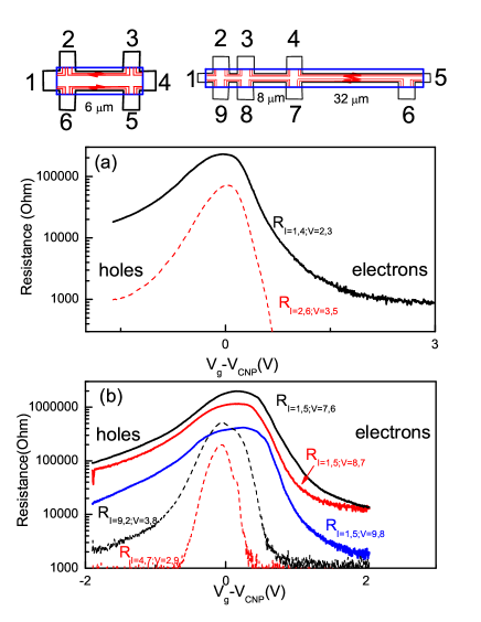
The density of the carriers in the HgTe quantum wells can be electrically manipulated with local gate voltage . The typical dependence of the four-terminal resistance of two of the representative samples A and B as a function of is shown in Figure 2. The resistance of the sample A and resistances for sample B, measured by various voltage probes in a zero magnetic field reveal a sharp peaks, shown in figure 2 a and b, when the gate voltage induces an additional charge density, altering the quantum wells from an n-type conductor to a p-type conductor via a 2D TI state. It has been shown konig ; buhmann that the 4-probe resistance in an HgTe/CdTe micrometer-sized ballistic Hall bar demonstrated a quantized plateaux . It is expected that the scattering between the helical edge states in the topological insulator is unaffected by the presence of a weak disorder kane ; bernevig ; hasan . Note, however, that the resistance of samples longer than might be much higher than due to the presence of the electron spin flip backscattering on each boundary. Mechanism of the back scattering is not clear and appealing task for theoreticians and a matter of ongoing debate vayrynen ; maciejko2 ; strom . The Hall effect reverses its sign and (not sown) when longitudinal resistance approaches its maximum value, which can be identified as the charge neutrality point (CNP). These behaviour is similar to those described in graphene sarma . An unambiguous way to prove the presence of edge state transport mechanism in 2D TI with strong backscattering on the boundary are the nonlocal electrical measurements. The nonlocal response always exists because of the presence of the two counter-propagating edge states, which flows sideways and may reach any contacts in the device roth ; gusev . Figures 2 a and b show the nonlocal resistances corresponding to the different configurations. For example, nonlocal resistance in figure 2a corresponds to the contact configuration, when the current flows between contacts 2 and 6 and the voltage is measured between contacts 3 and 5. One can see that the nonlocal resistance near CNP has a peak of a comparable amplitude, though less wide, and approximately in the same position as the local resistance. Outside of the peak the nonlocal resistance is negligibly small. The apparent residual nonlocal resistance in figure 2b above and below is is related to the noise in the full linear scale measurements.
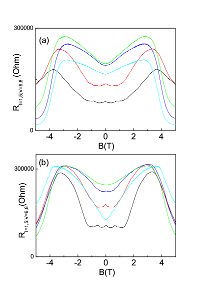
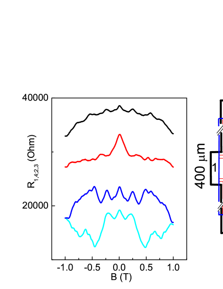
It is expected that a magnetic field perpendicular to the quantum well breaks time reversal symmetry (TRS) and thereby enables elastic scattering between counterpropagating chiral edge modes. However, a number of the different theoretical models has previously been proposed konig ; tkachov ; scharf ; chen ; maciejko2 with substantially different physical scenarios. In our previous study gusev2 we have observed a linear negative magnetoconductance in HgTe-based quantum wells in the 2D TI regime near CNP, when the edge state transport prevails. Our observation agrees with the model maciejko2 which describes the effects of WAL (see discussion section below for more details). The model predicts almost linear positive magnetoresistance , where parameter A strongly depends on the disorder strength W in comparison with the energy gap : the fluctuations result in a large B-slope corresponding to a strong disorder regime and fluctuations lead a small B-slope. Figure 3 shows the evolution of the resistance with magnetic field and density, when the chemical potential crosses the bulk gap. The magnetoresistance (MR) demonstrates a striking V-shape dependence in magnetic fields below 1T near CNP, which confirms our previous observations. Note however, that the V-shaped magnetoresistance is strongly transformed, when Fermi energy moves away from CNP to the electronic side of the resistance peak. In this region MR inverses the sign near zero magnetic field and shows triangular-shaped peak accompanied by two satellite features or damped oscillations. The width of the negative magnetoresistance spike and the period of the oscillations are slightly varied from sample to samples, as one can see in figures 3a and b. Both samples are almost identical with approximately equal mobility. Note that the Fermi level still lies in the bulk gap and transport is dominated by edge states, because we see nonlocal effects. In the hole side of the peak we do not find neither small negative magnetoresistance near B=0, nor the oscillations on the side branches of the the positive magnetoresistance. In magnetic fields above 3 T the magnetoresistance falls off rapidly marking a pronounced crossover to the quantum Hall effect regime in accordance with previous observations gusev2 .
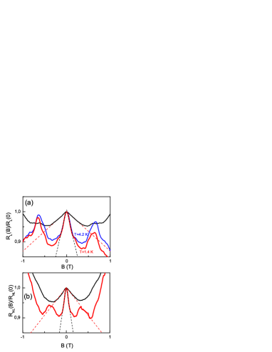
The figure 4 shows the low-fled part of the relative magnetoresistance for the two values of the gate voltages and two temperatures. One can see that for this particular sample the MR varies linearly with magnetic field. As voltage increases, the B-slope of the MR decreases and additional oscillation emerges. The MR profile does not show any significant temperature dependence. Figure 4 b displays traces of the resistance in nonlocal configuration for device B (). One can see similar triangular-shaped MR peak, as in the local geometry, though less wide, with two satellite peaks. Coexistence of the low-field negative MR peak in nonlocal configuration exclude the possibility that this effect has a bulk origin. It is worth noting , however, that around B=0 the magnetoresistance is parabolic rather than linear in nature.
Finally we present the results for a device C with a large gate. We expect that the length of the edge states in this structure is determined by the perimeter of the sample covered by the metallic gate. Figure 5 shows schematic view of the sample. One can see that the current flows mostly along the edges of the side branches. The resistance reveals saw-tooth oscillations, shown in Fig.5, when the Fermi energy passes the electronic side of the resistance peak away from CNP. Note, however, that the evolution of the oscillations with gate occurs rapidly and not gradually, as in devices A and B.
III Discussion
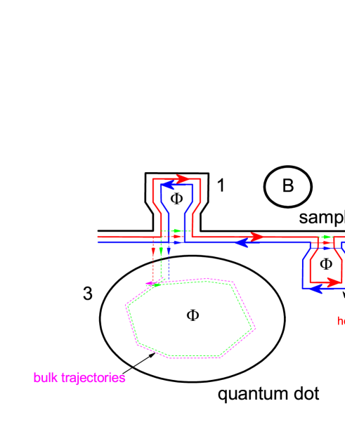
We now proceed to an analysis of the data described. We will focus on the two models that can explain the magnetoresistance of one dimensional edge electrons. Both models considered alternative paths for the edge states due to bulk disorder or rough edges of the realistic sample. Figure 6 illustrates the helical edge states in a disordered 2D TI in an uniform magnetic field. The first scenario describes disordered spinless one dimensional quantum wire maciejko2 . For strong enough disorder electron paths frequently deviate into the bulk region enclosing AB flux before returning back to the edge, labeled in figure 6 by number 2. The conventional WAL approach can be used. The average with respect to the different size of the loops leads to the positive linear magnetoresistance. Second scenario relies to the localization of the helical edge sates due to the collective action of the random magnetic flux through the loops, naturally formed by rough edges of the sample (labeled by number 1 in the Figure 6) deplace . In accordance with this scenario immediately after magnetic field is switched on, edge states become localized. The magnetic field penetrates through the random helical edge states loops (Figure 6 ), which acts as magnetic flux impurity and introduces the backscattering between edge states on each boundary. Similar to the first scenario the average with respect to the different magnetic fluxes should be performed. The model deplace predicts positive magnetoresistance and dependence of the inverse localization length in small magnetic field, which becomes more linear with increasing magnetic field. Our experimentally observed linear positive magnetoresistance near CNP are in good qualitative agreement with both models. Detailed comparison with model maciejko2 has been performed in our previous publication gusev . Discrimination among two scenarios requires further experimental work. It is worth noting that both models consider ballistic transport at zero magnetic field, while our samples demonstrate diffusive transport. Despite the fact that while the both models give a satisfactory description of the linear positive magnetoresistance near CNP, the explanation of negative MR and AB-like oscillations in Fig.3-4 away from CNP requires a further elaboration of the models.
Absence of the resistance quantization in samples with dimensions above a few microns konig ; buhmann ; gusev is another unsolved problem. One of the possible explanation is the fluctuations of the local insulating gap width induced by smooth inhomogeneities, which can be represented as metallic puddles or dots. The well-localized metallic regions along the edge have been found using scanning gate microscopy konig2 and in microwaves experiments kvon2 . According to the model vayrynen charge carrier puddles coupled to a coherent conductor results in incoherent inelastic processes and modifies the ballistic transport. Therefore metallic puddles can lead to spin dephasing, since an electron entering the puddle is thermalized by dissipation and later on fed back into the system. Therefore ballistic coherent transport is expected only in the region between the puddles, and total 4-terminal resistance exceeds the quantized value. Self-averaging resistance of the sample with edge state dominated contribution to transport is given by vayrynen :
| (1) |
where is the density of the puddles, is the electron penetration depth into the puddles ( is the electron velocity, is the forbidden gap), g is the dimensionless conductance within the dot (puddle), is the mean level spacing within the dot, L is the distance between probes (length of the edge states). It has been found that the equation 1 gives a satisfactory explanation of the high resistance value, obtained in experiments gusev3 . Combining all parameters we calculate , which is comparable with experimental value . The density of the puddles increases, and the size of the puddles is growing, when the Fermi level lies nearer to the conductive band. The Figure 6 illustrates the helical edge states in the presence of the all types of the disorder: edge roughness (1), bulk disorder (2) and metallic puddles due to inhomogeneous charge distributions. We ague that, while the edge roughness as well as the bulk disorder are important and play a dominant role in the region near CNP in magnetic field, away from CNP the role of the metallic puddles in MR becomes more pronounced and essential. WL effects in ballistic cavities indeed has been studied both theoretically baranger and experimentally chang2 . The WL peak and periodic oscillations are observed which were attributed to the Aharonov-Bohm effect through a periodic orbit within the cavities. Therefore, it is naturally to explain the negative magnetoresistance and AB-like oscillations in figures 3,4 by existence of metallic ballistic puddles near the edge. It is worth noting that the Fermi energy of electrons in puddles lies in the parabolic part of the energy spectrum ( figure 1) because of the low density. Therefore, one would expect that the spin orbit coupling is weak, and magnetoresistance is negative in agreement with our observations. It is easy to estimate the characteristic sizes of these loops using the period of the oscillations in fig.3-4, which is T. Then the characteristic area of the loops is and respectively size is about 100 nm. Indeed this value agrees with estimations of the puddle size and density gusev3 and scanning gate microscopy konig2 . Note that for explanation of the negative sign of the MR the role of the bulk electrons in the puddles is emphasized, however the bulk state and edge state may co-exist (figure 6). The interplay between the topological insulators helical states and bulk electrons requires further theoretical study. When the Fermi level moves to valence band, it is expected that the puddles should be occupied by the holes. Note however, that both dephasing and spin relaxation times for holes are found to be much smaller than for electrons in similar conditions and WAL effect should be considerably smaller in agreement with our observations.
When the Fermi level lies in the conductive band, and transport becomes dominant by massive fermions with Dirac spectrum (figure 1), the weak antilocalization behaviour has been observed olshanetsky2 .
In conclusion, we observed interplay between positive and negative magnetoresistance, when Fermi level shifts with respect to the charge neutrality point, but still lies inside of the gap, and transport occurs via edge states. We consider three contributions to the magnetoresistance: edge state penetration to the bulk, edge state scattering by magnetic flux formed by rough edges, and WL of the bulk electrons in the puddles formed by inhomogeneous charge distributions. The negative magnetoresistance and AB-like oscillations are attributed to weak localization of the bulk electrons in the metallic puddles formed by fluctuation of the local insulating gap.
We thank O.K.Raichev for helpful discussions. A financial support of this work by FAPESP, CNPq (Brazilian agencies), RFBI and RAS programs ”Fundamental researches in nanotechnology and nanomaterials” and ”Condensed matter quantum physics” is acknowledged.
References
- (1) P. A. Lee, T. V. Ramakrishnan, Rev.Mod.Phys.57, 287 (1985).
- (2) M. Z. Hasan, C. L. Kane, Rev.Mod.Phys. 82, 2045 (2010); X-L. Qi, S-C. Zhang,Rev.Mod.Phys. 83, 1057 (2011)
- (3) X-L. Qi, S-C. Zhang, Phys.Today, Phys. Today 63(1), 33 (2010).
- (4) J. E. Moore and L. Balents, Phys. Rev. B 75 121306 (2007)
- (5) J. E. Moore, Nature (London) 464, 194(2010).
- (6) C. L. Kane and E. J. Mele, Phys. Rev. Lett. 95, 146802 (2005).
- (7) B. A. Bernevig, T. L. Hughes, and S. C. Zhang, Science 314, 1757 (2006).
- (8) J.Maciejko,T. L. Hughes,and S-C Zhang, Annu. Rev. Condens. Matter Phys. 2, 31 (2011).
- (9) Wen Yang and Kai Chang, Shou-Cheng Zhang, Phys.Rev.Lett. 100, 056602 (2008).
- (10) Kai Chang and Wen-Kai Lou, Phys. Rev.Lett. 106, 206802 (2011).
- (11) M. König et al, Science 318, 766 (2007).
- (12) H.Buhmann, Journal. Appl.Phys.,109, 102409 (2011).
- (13) B. L. Altshuler, D. Khmel’nitzkii, A. I. Larkin and P. A. Lee, Phys. Rev. B 22, 5142 (1980).
- (14) P. M. Ostrovsky, I. V. Gornyi, and A. D. Mirlin, Phys. Rev. Lett. 105, 036803 (2010).
- (15) G. Tkachov and E. M. Hankiewicz, Phys. Rev. B 84, 035444 (2011).
- (16) G. Tkachov, Phys. Rev. B, 88, 205404 (2013).
- (17) P. M. Ostrovsky, I. V. Gornyi, and A. D. Mirlin, Phys. Rev. B 86, 125323 (2012).
- (18) J. Maciejko, X-L. Qi, and S-C. Zhang, Phys. Rev. B 82, 155310 (2010).
- (19) P. Delplace, J. Li, and M. Büttiker, Phys. Rev. Lett. 109, 246803 (2012).
- (20) G. M. Gusev, E.B.Olshanetsky, Z. D. Kvon, N. N. Mikhailov and S. A. Dvoretsky, Phys. Rev. B 87, 081311(R), (2013).
- (21) J.I.Vayrynen, M.Goldstein, L.I.Glazman, Phys.Rev.Lett. 110, 216402 (2013).
- (22) Z. D. Kvon, E. B. Olshanetsky, D. A. Kozlov, et al., Pis’ma Zh. Eksp. Teor. Fiz. 87, 588 (2008) [JETP Lett. 87, 502 (2008)].
- (23) E. B. Olshanetsky, Z. D. Kvon, N. N. Mikhailov, E.G. Novik, I. O. Parm, and S. A. Dvoretsky, Solid State Commun. 152, 265 (2012).
- (24) G. M. Gusev, Z. D. Kvon, O. A. Shegai, N. N. Mikhailov, S. A. Dvoretsky, and J. C. Portal, Phys. Rev. B 84, 121302(R), (2011).
- (25) J. Maciejko, C. X. Liu, Y. Oreg, X. L. Qi, C. Wu, and S. C. Zhang, Phys. Rev. Lett. 102, 256803 (2009).
- (26) A.Ström, H.Johannesson, G.I.Japaridze, Phys. Rev. Lett. 104, 256804 (2010).
- (27) S. Das Sarma, Shaffique Adam, E. H. Hwang, Enrico Rossi, Rev. Mod. Phys., 83, 407 (2011).
- (28) A. Roth, C. Brne, H. Buhmann, L.W. Molenkamp, J. Maciejko, X.-L. Qi, and S.-C. Zhang, Science 325, 294 (2009).
- (29) B. Scharf, A. Matos-Abiague, and J. Fabian, Phys. Rev. B 86, 075418 (2012).
- (30) J.C. Chen, J. Wang, and Q.F. Sun, Phys. Rev. B 85 125401 (2012).
- (31) M. Konig, M. Baenninger, A. G. F. Garcia et al., Phys. Rev. X 3, 021003 (2013).
- (32) Z.D.Kvon et al, Pisma v ZhETF,99, 333 (2014).
- (33) G.M.Gusev, Z.D.Kvon,E.B.Olshanetsky, A.D.Levin, Y. Krupko, J. C. Portal, N.N.Mikhailov, and S.A.Dvoretsky, Phys. Rev. B 89, 125305 (2014).
- (34) E. B. Olshanetsky, Z. D. Kvon, G.M.Gusev, et al, JETP Lett,91, 347 (2010).
- (35) H. U. Baranger, R. A. Jalabert, and A. D. Stone, Phys. Rev. Lett. 70, 3876 (1993).
- (36) A. M. Chang, H. U. Baranger, L. N. Pfeiffer, and K.W. West, Phys. Rev. Lett. 73, 2111 (1994).