CW and pulsed electrically detected magnetic resonance spectroscopy at 263 GHz/12 T on operating amorphous silicon solar cells
Abstract
Here we describe a new high frequency/high field continuous wave and pulsed electrically detected magnetic resonance (CW EDMR and pEDMR) setup, operating at 263 GHz and resonance fields between 0 and 12 T. Spin dependent transport in illuminated hydrogenated amorphous silicon p-i-n solar cells at 5 K and 90 K was studied by in operando 263 GHz CW and pEDMR alongside with complementary X-band CW EDMR. Benefiting from the superior resolution at 263 GHz, we were able to better resolve EDMR signals originating from spin dependent hopping and recombination processes. 5 K EDMR spectra were found to be dominated by conduction and valence band tale states involved in spin dependent hopping, with additional contributions from triplet exciton states. 90 K EDMR spectra could be assigned to spin pair recombination involving conduction band tail states and dangling bonds as dominating spin dependent transport process, with additional contributions from valence band tail and triplet exciton states.
keywords:
Electrically detected magnetic resonance , conduction band tail , valence band tail , amorphous silicon , solar cell1 INTRODUCTION
Electrically detected magnetic resonance (EDMR) spectroscopy is a highly sensitive spectroscopic technique that probes the involvement of paramagnetic states in charge transport and loss mechanisms, while paramagnetic background signals are eliminated [1, 2, 3]. EDMR is up to 8 10 orders of magnitude more sensitive than conventional electron paramagnetic resonance (EPR) spectroscopy [4] and thus allows for investigating a small number of spins in low dimensional material systems and devices [4, 5, 6, 7, 8]. In addition, EDMR is regarded as one of the key technologies to realize quantum computing algorithms based on coherent manipulation and readout of electron spins in semiconductor samples [9, 10, 11, 12]. Due to its high selectivity and sensitivity, EDMR is ideally suited for the assignment and structural characterization of paramagnetic states determining charge transport and loss mechanisms in organic and Si solar cells [13, 14, 15, 16, 17, 18, 19, 20]. Recently, it was shown that the application range of EDMR as compared to continuous wave (CW EDMR) may be further boosted by pulsed (pEDMR) detection schemes [9, 11, 21, 22, 23, 24, 25, 26], which greatly increased the selectivity to different spin-dependent transport mechanisms and spin coupling parameters as well as the spectral resolution [27, 28, 29, 30, 31, 32, 33, 34, 36, 35]. Up to now most CW and pEDMR studies employed conventional X-band (9.4 GHz/350 mT) spectrometers. However, the spectral resolution at this field is often not sufficient to resolve g-tensor anisotropies and the resonances of different overlapping paramagnetic states, having close proximity in g-values. This restriction may be lifted by high frequency/high field EDMR, which is capable of resolving small g-tensor anisotropies and overlapping EDMR resonances with slightly different g-values when the anisotropic Zeeman interaction, (g/g)B0 exceeds the field independent inhomogeneous broadening, B, i.e. (g/g)B0 B, where g is the g-value difference, g is the mean g-value and B0 is the external magnetic field.
A very first report on high frequency/high field CW EDMR appeared as early as 1978 in which Honig studied phosphorus doped crystalline Si (c-Si:P) at 196 GHz/7 T and a temperature of 1.4 K [37]. This work was extended in a later 240 GHz/8.6 T EDMR study on c-Si:P at T = 2.8 K [38, 39], where it was shown that the dominating spin-dependent transport process at very high fields and low temperatures is a direct capture of conduction band electrons by phosphorus states, while spin-pair formation dominates the low-field EDMR spectra in this system [9]. This important finding demonstrates that high frequency/high field EDMR increases not only the spectral resolution, but also the selectivity to particular transport processes.
A further W-band (94 GHz/3.4 T) EDMR study on a donor-doped metal-oxide-semiconductor device employing a single mode cavity at 5 K was reported by Lo [12, 40]. In this study sample dimensions were of sub-millimeter range to fit a W-band single mode resonator. Due to the superior resolution of high frequency/high field EDMR, the donor and the two dimensional electron gas (2-DEG) EDMR spectra, which overlap at X-band frequencies, could be separated. Very recently Meier conducted a multi-frequency (X-band, Q-band and W-band) pEDMR study on micro-crystalline (µc-Si:H) p-i-n solar cells with a-Si:H n-layer [19]. Thereby, the g-values and line shapes of a-Si:H conduction band tail states and localized µc-Si:H conduction band (CE) states could be determined with increased resolution. In order to further push the capabilities of very high frequency/high field EDMR, with respect to the accessible resonance frequencies/fields and temperatures, within this work we developed a CW EDMR/pEDMR set-up based on a commercial Bruker E-780 1016 EPR spectrometer working at 263 GHz/12 T. Herein, we give a detailed description of this instrument and demonstrate first 263 GHz CW EDMR and pEMDR experiments on operating a-Si:H p-i-n solar cells.
2 EDMR SPECTROMETER 263 GHz
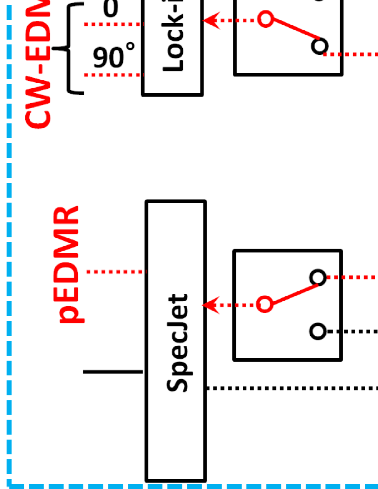
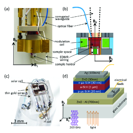
Fig. 1 shows the layout of the excitation and detection scheme of the 263 GHz spectrometer including the newly implemented CW EDMR/pEDMR extension. The depicted EDMR setup is based on a commercial Bruker E-780 1016, 263 GHz/12 T EPR spectrometer, which can be operated in CW and pulsed EPR and electron-nuclear double resonance (ENDOR) modes. Microwave (mw) generation and manipulation is done in a heterodyne microwave bridge. The corresponding resonance fields are generated in a cryogen-free superconducting magnet, which consists of a main and a sweep coil. The main solenoid coil can be swept between 0 and 12 T, while the sweep coil generates additional fields of 0.15 T with high accuracy. The latter can be driven in a special linearize mode to compensate for field nonlinearities. EDMR samples are placed in a non-resonant EPR/EDMR probe which is depicted in Fig. 2, with a photograph of the probe in Fig. 2a. Fig. 2b sketches the cross section of the probe showing the corrugated waveguide tapered down to the sample space, the position of the laser fiber for light excitation of the sample, the modulation coil (maximum modulation amplitude 50 G 100 kHz) and the sample position with the electrical contacts for EDMR detection. Inside the probe, sample temperature can be controlled between 4.5 K to 300 K using an Oxford ITC 503 temperature controller.
Fig. 2c shows the p-i-n solar cell sample of dimension mm (active solar cell area) that is attached to the sample holder. Electrical connections to the solar cell are realized by thin gold wires fixed using silver paste on the contact pads and finally soldered to the coaxial line, which is used to apply a constant voltage and to monitor the photocurrent from the sample. The layer structure of the p-i-n solar cell is depicted in Fig. 2d. It consists of a 1 µm thick intrinsic a-Si:H layer, which is sandwiched between thin p-type (20 nm) and n-type (30 nm) µc-Si:H layers and Al doped ZnO layer, that act as transparent conducting oxide contacts. We have used µc-Si:H as contact layers to distinguish signals from the p and n doped layers from that of the intrinsic a-Si:H layer as the two materials have different EDMR resonances [13, 14, 28]. Photo excitation of the solar cell is achieved by laser sources or the light from a 250-watt KL 2500 LCD halogen cold light source through a 1.22 mm optical fiber. The optical illumination and mw excitation of the solar cell is done through the glass substrate as depicted in the Fig. 2d. The details of the current detection setup are shown in Fig. 1. Here a steady-state photocurrent is established under a constant voltage bias (V) and illumination. The output of the trans-impedance amplifier (I-V convertor) converts the photocurrent into a voltage which goes through the filtering and amplification circuit (shown in the Fig. 1 in red blocks) to maximize the signal-to-noise ratio. This set-up allows for both CW EDMR as well as pEDMR detection. For CW EDMR detection, the current detection output is connected to either the absorption or dispersion channel of the Lock-In detector. Since the output of the Lock-In provides 4 channels (0∘ and 90∘ of the EPR absorption and dispersion signals, respectively), EPR and EDMR signals can be measured simultaneously. For pEDMR we directly connect the output of the current detection to one of the channels of the Bruker SpecJet digitizer (bandwidth 500 MHz). The maximum mw power available in CW as well as in pulse mode is 15 mW. The current transient after the mw pulse is boxcar integrated and recorded as a function of magnetic field to yield the pEDMR spectrum [3].
The current set-up allows for pulsed and CW EDMR with magnetic field and mw amplitude modulation as well as electrically detected electron electron double resonance (EDELDOR) [25], electrically detected electron nuclear double resonance (EDENDOR) [26] and electrically detected double electron electron resonance (EDDEER) [36]. These experiments carried out without the employment of a resonator holds great advantage as fully processed samples of several mm size may be mounted, temperature induced instabilities are less pressing as compared to single mode resonator set-ups and in addition it provides more freedom to add additional electrical connections, rf coils or illumination facilities. However, omitting a resonator significantly reduces the mw field at the sample position. For the solar cell used in this study, mw excitation has to be done through the glass substrate (see Fig. 2d) which further leads to nearly 10 dB loss in mw power. Even with the above mentioned losses, the minimum /2 pulse length achievable in the current EDMR set-up (15 mW at the entrance of the corrugated waveguide) is 1 µs, which corresponds to an excitation bandwidth of 1 MHz. This puts a restriction to perform pEDMR on samples with short relaxation times as well as on the detection of electron spin echo envelop modulation, ESEEM (nuclear Larmor frequency at 9.4 T for 15N 41 MHz, 29Si 80 MHz, 31P 162 MHz and 1H 400 MHz). In future, changing the sample design such that the mw excitation can be realised from the front side, we will be able to avoid the loss due to glass substrate. With such a design shorter /2 pulses will be possible that will increase the application range of pEDMR experiments.
The possibility to measure EPR and EDMR simultaneously in the current set-up greatly improves the accuracy of field calibrations, since for the precise determination of g-values reference EPR measurements with field standards (in our case Mn2+ in MgO matrix [41] or NC60 [42]) are required. These calibrations only yield optimum precision if the reference EPR sample can be placed exactly at the same position as the EPR/EDMR sample under study. Mounting and demounting of the reference sample may fail to reproduce the sample position. In order to circumvent this problem we attached a small amount of NC60 underneath the solar cell and recorded its EPR alongside with the EDMR.
3 EXPERIMENTAL RESULTS AND DISCUSSION
Fig. 3 depicts X-band CW and 263 GHz CW and pEDMR spectra obtained on illuminated a-Si:H solar cells under forward bias (V = +1 V) at 5 K and 90 K, respectively. For better comparability, all spectra are plotted against the same g-value span (upper x-axes) and the corresponding magnetic field values (bottom x-axes). In the following, we will first qualitatively describe the characteristics and differences of the EDMR spectra shown in Fig. 3. Based on these findings we will than conclude on the underlying spin dependent transport processes and finally test these assignments by spectral simulations.
X-band CW EDMR spectra measured at 5 K (Fig. 3a) and 90 K (Fig. 3b) are very similar. Both spectra are dominated by asymmetric lines centered at g = 2.0044 and g = 2.005, respectively, which extend towards larger g-values around g = 2.01. In addition, we find a very broad resonance (width 20 mT) centered around g = 2.008, which clearly exceeds the spectral window depicted in Fig. 3a and 3b. This contribution is more pronounced in the 5 K spectrum as compared to 90 K. Differences between 5 K and 90 K CW EDMR spectra obtained on the same solar cells under similar operating conditions strongly increase upon increasing the resonance frequency from X-band to 263 GHz. The 263 GHz CW EDMR spectrum measured at 5 K (Fig. 3c), now exhibits three well resolved contributions around g = 2.01 and g = 2.0044 and a smaller signal at g = 1.996. Plotting 5 K X-band and 263 GHz CW EDMR spectra on the same g-scale reveals a pronounced increase of the spectral resolution, despite of the fact that the individual spectral contributions significantly broaden. On the contrary, 90 K CW X-band and 263 GHz spectra (see Fig. 3b and 3d) have very similar shapes. Their main difference is an increase of the absolute spectral width at 263 GHz.
Observed temperature induced differences between 5 K and 90 K 263 GHz CW EDMR spectra are a clear indication that the spectra are dominated by different paramagnetic states and hence different spin dependent transport processes, despite of their similarity at X-band frequencies. Additional information on the prevailing spin dependent transport process may be obtained from complementary pEDMR measurements. 5 K and 90 K 263 GHz pEDMR spectra are depicted in Fig. 3e and 3f, respectively. 263 GHz pEDMR and CW EDMR spectra exhibit identical spectral contributions. However, in addition to temperature induced spectral changes 5 K and 90 K pEDMR spectra exhibit different signs. At 5 K, 263 GHz pEDMR induces a current enhancement (positive signal), whereas at 90 K pEDMR current quenching (negative signal) is observed.
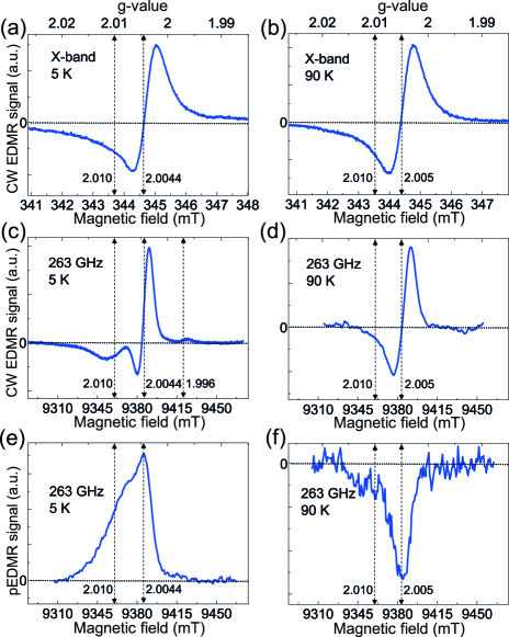
We will now identify the observed resonances with paramagnetic states and assign them to spin dependent transport pathways. Intrinsic a-Si:H is a disordered semiconductor with localized states below the conduction and above the valence band, which are referred to as conduction band tail (cbt) and valence band tail (vbt) states. Under illumination cbt and vbt become paramagnetic [43, 44, 45, 46, 47]. For cbt states in a-Si:H, multi-frequency pEDMR up to W-band frequencies revealed a purely isotropic g-value (g = 2.0047(2)) [19]. For the vbt counterpart, the situation is less clear. This state is typically associated with a resonance at g = 2.011 [43, 44, 45]. However, Q-band EPR on illuminated intrinsic a-Si:H powders revealed pronounced g-tensor anisotropy for vbt states (gxx = 2.019, gyy = 2.012 and gzz = 2.005) [47]. Furthermore, it was concluded that vbt g-values depend on the p-type doping level and the sample temperature [48]. However, till date latter assignments have not been confirmed by high frequency EPR or EDMR.
At liquid He temperatures spin dependent hopping transport along cbt and vbt gives rise to EDMR induced current enhancement spectra [13, 49, 50, 16]. We therefore assign the 5 K EDMR enhancing signals plotted in Fig. 3a, 3c and 3e, to two independent spin dependent hopping processes along cbt (g = 2.0044) and vbt (g = 2.011) states, respectively. The small signal at g = 1.996 observed in 5 K 263 GHz CW EDMR spectra (Fig. 3c) can be assigned to a similar hopping process along CE states in the n-doped µc-Si:H layer [17, 28, 51, 52]. An additional very broad resonance (20 mT) centered around g = 2.008 has been observed by optically detected magnetic resonance [30, 53] and CW EDMR [49, 50] on undoped a-Si:H layer and was associated to strongly coupled triplet electron-hole (e-h) pairs. This triplet exciton signal may account for the broad background observed in the X-band CW EDMR spectrum (Fig. 3a).
Intrinsic a-Si:H exhibits further pronounced EPR and EDMR resonances, which have been associated to three fold coordinated Si atoms, so called dangling bonds (dbs) [45, 47, 54, 55]. At temperatures, between 70 K and room temperature, tunneling of trapped cbt electrons into neutral dbs leads to doubly occupied db (db-) states which finally recombine with holes [13, 49, 50, 16]. The same spin dependent recombination process gives rise to the 90 K EDMR spectra depicted in Fig. 3b, 3d and 3f. The peak of the main resonance position at g = 2.005, is a superposition of the db (g = 2.0055) and cbt (g = 2.0044) resonances. In pEDMR, this process leads to a current quenching signal (see Fig. 3f). It should be noted here that the sign change between 5 K and 90 K is not evident in the CW EDMR spectra mainly because the phase of the CW EDMR spectra has complex dependence on experimental conditions such as temperature, microwave power and modulation frequency [56]. 90 K EDMR spectra still show contributions from vbt resonances. This is most obvious in the 90 K X-band CW EDMR spectrum depicted in Fig. 3b, but can be also found in the 90 K 263 GHz pEDMR current quenching spectrum (Fig. 3f). Similar signals were previously assigned to a recombination process, where the final electron-hole recombination step occurs between a doubly occupied db- and a hole trapped in a vbt state. This step may be enhanced by spin-dependent diffusion of holes via vbt states towards the db- [45].
To further test these assignments, we performed numerical simulations of the experimental EDMR spectra using Easyspin, a Matlab EPR simulation toolbox [57]. In the simulations, the individual EDMR resonances were modeled by isolated spin centers, for which only the respective Zeeman interaction was explicitly taken into account in the Spin Hamiltonian. Any spin-spin interaction between different centers was neglected. Line width parameters for S = 1/2 centers (cbt, vbt and db) were modeled using site-to-site g-value variations (g-strain) in combination with field independent Gaussian or Lorentzian lines. The latter combination leads to Voigtian line shapes at X-band frequency, with increasing Gaussian contribution at 263 GHz. For triplets (S = 1), a field independent dipolar broadened Gaussian line shape was assumed. In cases where independent processes contribute to the EDMR spectrum, e.g. for spin dependent hopping among vbt and cbt states, the weights of the resonances were determined individually. However, for spectra in which two resonances contribute to the same process, e.g. spin dependent recombination from cbt to dbs, the same weights were used for both spin pair partners.
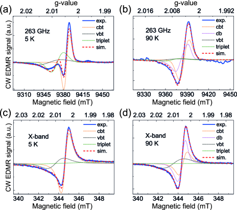
Since 5 K and 90 K EDMR spectra are resulting from different spin dependent processes, different models were employed to simulate low and high temperature EDMR spectra. Based on the above assignments, we started to simulate the 5 K 263 GHz CW EDMR spectrum as a superposition of isotropic cbt (g = 2.0044) and vbt (g = 2.011) states and an additional contribution from triplet excitons (g = 2.008). To adjust the line intensities and widths of the simulation to the experimental 5K 263 GHz CW EDMR spectrum, a fitting routine was employed in which the line widths and weights were left open. Fig. 4 depicts simulated and experimental EDMR spectra alongside with the individual contributions of different spin centers. Best fits to the 5K 263 GHz CW EDMR spectrum (Fig. 4a) were achieved using a field independent Lorentzian line with full-width-half-maxima of 1 mT (1.5 mT), field dependent g-strain of 0.0025 (0.01) for cbt (vbt) lines and a 26 mT broad Gaussian line for the triplet exciton signal. Using the same g-values and line width parameters, but different weights for the single paramagnetic states, we were also able to reproduce the main features of 5 K X-band CW EDMR spectrum (Fig. 4c). However, in both cases we find deviations between simulated and experimental EDMR spectra. These differences are most pronounced at the low field edges of the spectra in the range of the vbt resonances. To test whether these discrepancies may originate from an anisotropic vbt g-tensor, we performed additional spectral fits to the 263 GHz CW EDMR spectrum assuming isotropic cbt and triplet signals, but anisotropic vbt g-values. In the fits all three main components of the vbt g-tensor and the isotropic cbt g-values were left open. A much better agreement between experimental and calculated spectra, as compared to the purely isotropic assumption, were obtained for a cbt g-value = 2.00445(6) and an anisotropic vbt g-tensor with gxx = 2.015(1), gyy = 2.009(1) and gzz = 2.0058(2) (not shown).
The observed vbt g-tensor anisotropy is in accordance with previous Q-band EPR experiments on illuminated a-Si:H powders [47]. However, vbt g-values, extracted from spectral fits to the 263 GHz CW EDMR spectra, significantly deviate from those extracted by EPR [47]. Notably, the largest canonical g-value, gxx = 2.015 deviates from gxx = 2.019, the value obtained in Ref. [47]. Despite the fact that our 263 GHz EDMR approach spreads g-values over a much wider spectral window and thereby potentially provides more accurate g-values, different reasons may be responsible for the observed discrepancy. It may be due to different experimental conditions and detection techniques or the presence of additional yet unassigned paramagnetic states involved in other spin dependent transport processes. In particular, the latter point cannot be unambiguously discriminated from a vbt g-tensor anisotropy based on the experimental data presented herein.
Finally, we simulated the CW EDMR spectra obtained at 90 K assuming spin dependent recombination between cbt and db states as dominating process, with additional contributions from vbt states and triplet excitons. g-values, g-strains and field independent line width parameters of cbt, vbt and triplet states were chosen identical to those extracted from spectral fits (based on isotropic g-values of cbt and vbt states) to the 5 K 263 GHz EDMR spectrum (see above). The db g-tensor (gxx = 2.0079, gyy = 2.0061 and gzz = 2.0034) and strains were taken from Ref. [55]. To simulate the experimental 90 K 263 GHz and X-band CW EDMR spectrum, a fitting routine was employed in which the weights of the individual lines were left open, with the restrictions that cbt and db weights are assumed to be the same. Fig. 4b and 4d depict experimental 263 GHz and X-band 90 K CW EDMR spectra, respectively alongside with the contributions of the individual spin centers. Good match between simulated and experimental EDMR spectra confirm the assignment of paramagnetic states contributing to the spectrum.
4 CONCLUSION
In conclusion, we have developed a 263 GHz/12 T CW/pEDMR set-up which allows for in-situ measurements on fully processed electronic devices under light and applied bias voltage. With this set-up, EDMR measurements can be realized from liquid He to room temperatures. Precise magnetic field calibration at the sample position can be obtained by simultaneous EPR measurements of reference samples attached to EDMR samples.
Based on these achievements in EDMR instrumentation we performed first 263 GHz CW/pEDMR on a fully processed a-Si:H p-i-n solar cell. In comparison with X-band CW EDMR, these measurements allowed for an assignment of the dominating paramagnetic centers and spin dependent transport processes at 5 K and 90 K. At 5 K EDMR signals could be identified with hopping transport along cbt and vbt states and an additional contribution from triplet states. At 90 K spin dependent recombination from cbt into dbs was found to dominate, superimposed by additional vbt and triplet signals. Spectral simulations based on these assumptions and line shape parameters obtained from literature reproduced the experimental X-band and 263 GHz spectra differently well. 90 K X-band and 263 GHz data could be simulated very well. However, we found discrepancies between experimental and simulated 5 K EDMR spectra assuming contributions from cbt, vbt and triplet states. First tentative simulations revealed that this discrepancy may either originate from a pronounced anisotropy of the vbt g-tensor or the contribution of additional yet unassigned paramagnetic states. A clear cut assignment of the involved centers requires additional pulsed multi-frequency EDMR experiments, which would allow for a discrimination between S = 1/2 and S = 1 spins [29, 58]. Such studies are currently on the way in our lab. Additional evidence may be gained from complementary advanced density functional theory calculations, which became available only recently and were employed for the g-tensor calculations of cbt and db in a-Si:H [18, 55, 34]. In the present case, calculations of vbt g-values could provide important additional information on whether vbt states indeed exhibit anisotropic g-values. The presented results demonstrate that multi-frequency EDMR, including very high frequencies up to 263 GHz, can help to resolve overlapping EDMR resonances and to assign transport processes involving the same or different paramagnetic states. Combing the high versatility of pEDMR with respect to mw excitation schemes with the ultimate sensitivity of CW EDMR in a high frequency/high field EDMR experiment further boosts the potential of this approach. Due to its unmatched detection sensitivity, such studies are not limited to cryogenic temperatures but may in the future also be performed at room temperature, which will yield further highly desired pieces of information on spin dependent transport processes in operating electronic devices.
5 ACKNOWLEDGEMENT
This work was supported by the German Research Foundation within SPP 1601. We thank F. Finger and O. Astakhov (Forschungszentrum Jülich) for supplying the solar cells which were prepared through the BMBF funded network project EPR-Solar (03SF0328). We are also grateful to J. Behrends (FU Berlin HZB) for helpful discussions.
References
References
- [1] D. J. Lepine, Spin dependent recombination on silicon surface, Phys. Rev. B 6, 436-441 (1972).
- [2] D. Kaplan, I. Solomon, and N. F. Mott, Explanation of the large spin-dependent recombination effect in semiconductors, J. Phys. (Paris) 39, 51-54 (1978).
- [3] C. Boehme and K. Lips, Theory of time-domain measurement of spin-dependent recombination with pulsed electrically detected magnetic resonance, Phys. Rev. B 68, 245105-245109 (2003).
- [4] D. R. McCamey, H. Huebl, M. S. Brandt, W. D. Hutchison, J. C. McCallum, R. G. Clark and A. R. Hamilton, Electrically detected magnetic resonance in ion-implanted Si:P nanostructures, Appl. Phys. Lett. 89, 182115-182117 (2006).
- [5] M. Xiao, I. Martin, E. Yablonovitch, and H. W. Jiang, Electrical detection of the spin resonance of a single electron in a silicon field-effect transistor, Nature 430, 435-439 (2004).
- [6] T. Umeda, Y. Mochizuki, K. Okonogi, K. Hamada, Electrically detected magnetic resonance of ion-implantation damage centers in silicon large-scale integrated circuits, J. Appl. Phys. 94, 7106-7111 (2003).
- [7] S.Y. Lee, S. Y. Paik, D. R. McCamey, J. Hu, F. Zhu, A. Madan and C. Boehme, Spin-dependent processes in amorphous silicon-rich silicon-nitride, Appl. Phys. Lett. 97, 192104-192104 (2010).
- [8] S. Paleari, S. Baldovino, A. Molle, and M. Fanciulli, Evidence of trigonal dangling bonds at the Ge(111)/Oxide interface by electrically detected magnetic resonance, Phys. Rev. Lett. 110, 206101-206105 (2013).
- [9] A. R. Stegner, C. Boehme, H. Huebl, M. Stutzmann, K. Lips and M. S. Brandt, Electrical detection of coherent 31P spin quantum states, Nature Phys. 2, 835-838 (2006).
- [10] H. Morishita, E. Abe, W. Akhtar, L. S. Vlasenko, A. Fujimoto, K. Sawano, Y. Shiraki, L. Dreher, H. Riemann, N. V. Abrosimov, P. Becker, H. J. Pohl, M. L. W. Thewalt, M. S. Brandt, and K. M. Itoh, Linewidth of low-field electrically detected magnetic resonance of phosphorus in isotopically controlled silicon, Appl. Phys. Exp. 4, 021302 (2011).
- [11] D. R. McCamey, J. Van Tol, G. W. Morley and C. Boehme, Electronic spin storage in an electrically readable nuclear spin memory with a lifetime 100 seconds, Science 330, 1652-1656 (2010).
- [12] C. C. Lo, V. Lang, R. E. George, J. J. L. Morton, A. M. Tyryshkin, S. A. Lyon, J. Bokor, and T. Schenkel, Electrically detected magnetic resonance of neutral donors interacting with a two-dimensional electron gas, Phys. Rev. Lett. 106, 207601 (2011).
- [13] K. Lips and W. Fuhs, Transport and recombination in amorphous p-i-n type solar cells studied by electrically detected magnetic resonance, J. Appl. Phys. 74, 3993-3999 (1993).
- [14] M. Stutzmann, M. S. Brandt and M. W. Bayerl, Spin-dependent processes in amorphous and microcrystalline silicon: a survey, J. Non-Cryst. Solids 266, 1-22 (2000).
- [15] K. Lips, P. Kanschat and W. Fuhs, Defects and recombination in microcrystalline silicon, Sol. Energy Mat. Sol. Cells 78, 513-541 (2003).
- [16] R. Müller, P. Kanschat, S. von Aichberger, K. Lips and W. Fuhs, Identification of transport and recombination paths in homo and heterojunction silicon solar cells by electrically detected magnetic resonance, J. Non-Cryst. Solids 266, 1124-1128 (2000).
- [17] P. Kanschat, K. Lips and W. Fuhs, Identification of non-radiative recombination paths in microcrystalline silicon (µc-Si:H), J. Non-Cryst. Solids 266, 524-528 (2000).
- [18] B. M. George, J. Behrends, A. Schnegg, T. F. Schulze, M. Fehr, L. Korte, B. Rech, K. Lips, M. Rohrmüller, E. Rauls, W. G. Schmidt, and U. Gerstmann, Atomic structure of interface states in silicon heterojunction solar cells, Phys. Rev. Lett. 110, 136803 (2013).
- [19] C. Meier, J. Behrends, C. Teutloff, O. Astakhov, A. Schnegg, K. Lips, and R. Bittl, Multi-frequency EDMR applied to microcrystalline thin-film silicon solar cells, J. Magn. Reson. 234, 1-9 (2013).
- [20] K. Lips, C. Boehme and W. Fuhs, Recombination in µc-Si:H pin solar cells, J. Non-Cryst. Solids 338, 702-705 (2004).
- [21] C. Boehme and K. Lips, Electrical detection of spin coherence in silicon, Phys. Rev. Lett. 91, 246603 (2003).
- [22] C. Boehme and K. Lips, The ultra sensitive electrical detection of spin Rabi oscillation at paramagnetic defects, Physica B 376, 930-935 (2006).
- [23] J. Behrends, K. Lips and C. Boehme, Observation of precursor pair formation of recombining charge carriers, Phys. Rev. B 80, 045207 (2009).
- [24] H. Huebl, F. Hoehne, B. Grolik, A. R. Stegner, M. Stutzmann and M. S. Brandt, Spin Echoes in the charge transport through phosphorus donors in silicon, Phys. Rev. Lett. 100, 177602 (2008).
- [25] F. Hoehne, H. Huebl, B. Galler, M. Stutzmann and M. S. Brandt, Spin-dependent recombination between phosphorus donors in silicon and Si/SiO2 interface states investigated with pulsed electrically detected electron double resonance, Phys. Rev. Lett. 104, 046402 (2010).
- [26] F. Hoehne, L. Dreher, H. Huebl, M. Stutzmann and M. S. Brandt, Electrical detection of coherent nuclear spin oscillations in phosphorus-doped silicon using pulsed ENDOR, Phys. Rev. Lett. 106, 187601 (2011).
- [27] A. Schnegg, J. Behrends, M. Fehr and K. Lips, Pulsed electrically detected magnetic resonance for thin film silicon and organic solar cells, Phys. Chem. Chem. Phys. 14, 14418-14438 (2012).
- [28] J. Behrends, A. Schnegg, M. Fehr, A. Lambertz, S. Haas, F. Finger, B. Rech and K. Lips, Electrical detection of electron spin resonance in microcrystalline silicon pin solar cells, Philos. Mag. 89, 2655-2676 (2009).
- [29] J. Behrends, A. Schnegg, K. Lips, E. A. Thomsen, A. K. Pandey, I. D. W. Samuel, and D. J. Keeble, Bipolaron formation in organic solar cells observed by pulsed electrically detected magnetic resonance, Phys. Rev. Lett. 105, 176601 (2010).
- [30] T. W. Herring, S. Y. Lee, D. R. McCamey, P. C. Taylor, K. Lips, J. Hu, F. Zhu, A. Madan and C. Boehme, Experimental discrimination of geminate and non-geminate recombination in a-Si:H, Phys. Rev. B 79, 195205 (2009).
- [31] F. Friedrich, C. Boehme and K. Lips, Triplet recombination at Pb centers and its implications for capture cross sections, J. Appl. Phys. 97, 056101 (2005).
- [32] C. Boehme, J. Behrends, K. v. Maydell, M. Schmidt and K. Lips, Investigation of hopping transport in n-a-Si:H/c-Si solar cells with pulsed electrically detected magnetic resonance, J. Non-Cryst. Solids 352, 1113-1116 (2006).
- [33] M. Fehr, J. Behrends, S. Haas, B. Rech, K. Lips and A. Schnegg, Electrical detection of electron-spin-echo envelope modulations in thin-film silicon solar cells, Phys. Rev. B 84, 193202 (2011).
- [34] F. Hoehne, J. Lu, A. R. Stegner, M. Stutzmann, M. S. Brandt, M. Rohrmüller, W. G. Schmidt, and U. Gerstmann, Electrically detected electron-spin-echo envelope modulation: A highly sensitive technique for resolving complex interface structures, Phys. Rev. Lett. 106, 196101 (2011).
- [35] C. Meier, C. Teutloff, O. Astakhov, F. Finger, R. Bittl and J. Behrends, Electrically detected HYSCORE on conduction band tail states in 29Si-Enriched microcrystalline silicon, Appl. Magn. Reson. 45, 1075-1086 (2014).
- [36] M. Suckert, F. Hoehne, L. Dreher, M. Kuenzl, H. Huebl, M. Stutzmann and M. S. Brandt, Electrically detected double electron electron resonance: exchange interaction of 31P donors and Pb0 defects at the Si/SiO2 interface, Mol. Phys. 111, 2690-2695 (2013).
- [37] A. Honig and M. Moroz, Precision absolute measurements of strong and highly inhomogeneous magnetic fields, Rev. Sci. Instrum. 49, 183-187 (1978).
- [38] G. W. Morley, D. R. McCamey, H. A. Seipel, L. C. Brunel, J. van Tol, and C. Boehme, Long-lived spin coherence in silicon with an electrical spin trap readout, Phys. Rev. Lett. 101, 207602 (2008).
- [39] D. R. McCamey, J. van Tol, G. W. Morley, and C. Boehme, Fast nuclear spin hyperpolarization of phosphorus in silicon, Phys. Rev. Lett. 102, 027601 (2009).
- [40] V. Lang, C. C. Lo, R. E. George, S. A. Lyon, J. Bokor, T. Schenkel, A. Ardavan, and J. J. L. Morton, Electrically detected magnetic resonance in a W-band microwave cavity, Rev. Sci. Instrum. 82, 034704 (2011).
- [41] O. Burghaus, M. Rohrer, T. Gotzinger, M. Plato and K. Möbius, A novel high-field/high-frequency EPR and ENDOR spectrometer operating at 3 mm wavelength, Meas. Sci. Technol. 3, 765-774 (1992).
- [42] Private communication with Mika Pflüger and Robert Bittl, Freie Universität Berlin.
- [43] J. C. Knights, D. K. Biegelsen, and I. Solomon, Optically induced electron spin resonance in doped amorphous silicon, Solid State Commun. 22, 133-137 (1977).
- [44] R. A. Street, D. K. Biegelsen, and R. L. Weisfield, Recombination in a-Si: H: Transitions through defect states, Phys. Rev. B 30, 5861 (1984).
- [45] H. Dersch, L. Schweitzer, and J. Stuke, Recombination processes in a-Si:H: Spin-dependent photoconductivity, Phys. Rev. B 28, 4678 (1983).
- [46] T. Umeda, S. Yamasaki, J. Isoya, A. Matsuda, and K. Tanaka, Electronic structure of band-tail electrons in a-Si:H, Phys. Rev. Lett. 77, 4600 (1996).
- [47] T. Umeda, S.Yamasaki, J. Isoya, and K. Tanaka, Microscopic origin of light-induced ESR centers in undoped hydrogenated amorphous silicon, Phys. Rev. B 62, 15702 (2000).
- [48] H. Dersch, J. Stuke and J. Beichler, Electron Spin Resonance of Doped Glow-Discharge Amorphous Silicon, Phys. Stat. Sol. (b) 105, 265-274 (1981).
- [49] M. S. Brandt and M. Stutzmann, Spin-dependent conductivity in amorphous hydrogenated silicon, Phys. Rev. B 43, 5184(R) (1991).
- [50] K. Lips, S. Schütte and W. Fuhs, Microwave-induced resonant changes in transport and recombination in hydrogenated amorphous silicon, Philosophical Magazine Part B 65, 945-959 (1992).
- [51] J. Müller, F. Finger, R. Carius, and H. Wagner, Electron spin resonance investigation of electronic states in hydrogenated microcrystalline silicon, Phys. Rev. B 60, 11666 (1999).
- [52] M. M. de Lima, Jr., P. C. Taylor, S. Morrison, A. LeGeune, and F. C. Marques, ESR observations of paramagnetic centers in intrinsic hydrogenated microcrystalline silicon, Phys. Rev. B 65, 235324 (2002).
- [53] K. Morigaki, Recombination mechanisms in amorphous semiconductors deduced from resonance measurements, J. Non-Cryst. Solids 7778, 583-592 (1985).
- [54] M. Stutzmann and D. K. Biegelsen, Microscopic nature of coordination defects in amorphous silicon, Phys. Rev. B 40, 9834 (1989).
- [55] M. Fehr, A. Schnegg, B. Rech, K. Lips, O. Astakhov, F. Finger, G. Pfanner, C. Freysoldt, J. Neugebauer, R. Bittl, and C. Teutloff, Combined multifrequency EPR and DFT study of dangling bonds in a-Si:H, Phys. Rev. B 84, 245203 (2011).
- [56] S. Lee, S. Paik, D. R. McCamey, and C. Boehme, Modulation frequency dependence of continuous-wave optically/electrically detected magnetic resonance, Phys. Rev. B 86, 115204 (2012).
- [57] S. Stoll and A. Schweiger, EasySpin, a comprehensive software package for spectral simulation and analysis in EPR, J. Magn. Reson. 178, 42-55 (2006).
- [58] A. Gliesche, C. Michel, V. Rajevac, K. Lips, S. D. Baranovskii, F. Gebhard, and C. Boehme, Effect of exchange coupling on coherently controlled spin-dependent transition rates, Phys. Rev. B 77, 245206 (2008).