Distance dependence of the energy transfer rate from a single semiconductor nanostructure to graphene
Abstract
The near-field Coulomb interaction between a nano-emitter and a graphene monolayer results in strong Förster-type resonant energy transfer and subsequent fluorescence quenching. Here, we investigate the distance dependence of the energy transfer rate from individual, i) zero-dimensional CdSe/CdS nanocrystals and ii) two-dimensional CdSe/CdS/ZnS nanoplatelets to a graphene monolayer. For increasing distances , the energy transfer rate from individual nanocrystals to graphene decays as . In contrast, the distance dependence of the energy transfer rate from a two-dimensional nanoplatelet to graphene deviates from a simple power law, but is well described by a theoretical model, which considers a thermal distribution of free excitons in a two-dimensional quantum well. Our results show that accurate distance measurements can be performed at the single particle level using graphene-based molecular rulers and that energy transfer allows probing dimensionality effects at the nanoscale.
Keywords: graphene; semiconductor nanocrystals; quantum dots; semiconductor nanoplatelets; quantum wells; resonant energy transfer; FRET; single molecule luminescence; heterostructures; dimensionality
Introduction
Graphene and colloidal semiconductor nanostructures are model low-dimensional systems, which hold promise for opto-electronic applications Bonaccorso et al. (2010); Koppens et al. (2014); Talapin et al. (2010). On the one hand, graphene, as a quasi-transparent semi-metal Nair et al. (2008); Mak et al. (2008) with excellent transport properties Das Sarma et al. (2011), can be seen as an ultimate transparent electrode Wang et al. (2008a); Kim et al. (2009a). On the other hand, CSNs, in the form of zero-dimensional nanocrystals Edited by Klimov (2010) (NCs or quantum dots), one-dimensional quantum rods Peng et al. (2000) and two dimensional nanoplatelets Ithurria and Dubertret (2008); Ithurria et al. (2011) (NPs, or quantum wells), are very efficient broadband light harvesting systems and size tunable nano-emitters, which are intensively used in a new generation of light emitting diodes, solar cells and photovoltaic devices Talapin et al. (2010).
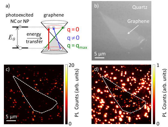
There is a growing interest in combining graphene and colloidal semiconductor nanostructures in the form of hybrid systems Chen et al. (2010); Ajayi et al. (2014); Rogez et al. (2014) and devices Konstantatos et al. (2012); Sun et al. (2012); Klekachev et al. (2012, 2013) with new functionalities and potentially enhanced opto-electronic properties. The photoresponse of the graphene NC-hybrid system is governed by interface and short-range phenomena, such as charge transfer and Förster-type resonant energy transfer Förster (1948) (RET) (see Figure 1). While photo-induced charge transfer may result in a photogating effect and improved photogain Konstantatos et al. (2012); Sun et al. (2012), energy transfer from a photoexcited colloidal semiconductor nanostructure (donor) to a graphene layer (acceptor) may efficiently generate electron-hole pairs in graphene, which is of interest for optoelectronics Koppens et al. (2014). Importantly, graphene stands out as a uniquely tunable acceptor system, in which distinct regimes of RET can be observed by varying its Fermi level Velizhanin and Efimov (2011); Gómez-Santos and Stauber (2011); Tielrooij et al. (2014); Lee et al. (2014).
Highly efficient RET from individual CdSe/ZnS NCs to graphene, resulting in a quenching of the luminescence signal by more than one order of magnitude, has recently been reported Chen et al. (2010). Related effects have been observed using other types of semiconductor nanostructures Ajayi et al. (2014); Rogez et al. (2014); Shafran et al. (2010); Jander et al. (2011); Lin et al. (2013), fluorescent molecules Treossi et al. (2009); Kim et al. (2009b); Gaudreau et al. (2013) or NV centers Stöhr et al. (2012); Tisler et al. (2013). The observation of robust and efficient RET to graphene has stimulated numerous applications in biosensing Wang et al. (2011) and holds promise for distance sensing Mazzamuto et al. (2014) and photodetection. The case of a single colloidal semiconductor nanostructure near a single layer of graphene is of particular interest, since it provides a well-defined and technologically relevant system, in which the sensitivity of the RET rate to the local environment and its distance dependence can be assessed with accuracy. In addition, RET is known to be strongly affected by exciton dimensionality and exciton localization Halivni et al. (2012); Rindermann et al. (2011). Colloidal semiconductor nanostructures offer natural ways to explore such effects.
Here, we investigate RET from i) individual core/shell CdSe/CdS NCs and ii) core/shell CdSe/CdS/ZnS NPs to a graphene monolayer. Using molecular beam epitaxy, we are able to deposit ultrasmooth dielectric spacers of magnesium oxide (MgO), with variable thickness, between graphene and the nanoemitters Godel et al. (2013). The scaling of the RET rate with the distance separating graphene from the nanoemitters is then quantitatively determined from the luminescence decays recorded on a collection of individual emitters. In the case of zero-dimensional NCs, the RET rate scales as , as expected theoretically Kuhn (1970); Chance et al. (1978); Swathi and Sebastian (2009); Gómez-Santos and Stauber (2011); Velizhanin and Efimov (2011); Gaudreau et al. (2013). Interestingly, although the RET rate of individual two-dimensional NPs adsorbed on bare graphene is similar to that observed with zero-dimensional NCs, we find that the RET rate decays less rapidly with increasing distance. Such a behavior is discussed within the framework of energy transfer from free two-dimensional excitons Basko et al. (2000); Kos et al. (2005) to a two-dimensional acceptor.
Methods
We have investigated individual colloidal semiconductor nanostructures near a graphene monolayer at room temperature, using a home-built micro-photoluminescence (PL) setup equipped with a air objective. Core/shell CdSe/CdS NCs ( in diameter, with peak emission at , i.e., photon energy of ), coated with oleylamine and oleic acid ligands, and core/shell/shell CdSe/CdS/ZnS NPs (4 monolayer thick core, thick shell, width, length and peak emission at , i.e., photon energy of ), coated with oleate ligands, were synthesized following previous works Mohamed et al. (2005); Mahler et al. (2008); Ithurria et al. (2011); Mahler et al. (2012); Tessier et al. (2013) (see also Supporting Information). Using core/shell structures dramatically reduces the possibility of irreversible photoinduced NC or NP ionization and subsequent charge transfer to graphene Hines and Guyot-Sionnest (1996); Tessier et al. (2013). NCs and NPs, dispersed at very low concentration into a hexane/octane mixture were then dropcast onto graphene samples.
Measurements on bare graphene (see Figures 1–3) were performed using mechanically exfoliated graphene monolayers deposited on transparent fused quartz substrates. The distance dependence of the energy transfer rate was investigated using large area graphene monolayers, grown by low-pressure chemical vapor deposition (LPCVD) on a copper foil, then transfered onto a fused quartz substrate using standard methods Li et al. (2009) (see Supporting Information). In order to vary the distance between graphene and the nano emitters, thin films of MgO were grown on top of graphene in a staircase fashion in a molecular beam epitaxy (MBE) chamber Godel et al. (2013) before deposition of NCs or NPs. We checked by atomic force microscopy that the roughness of the MgO layer is on the order of Wang et al. (2008b).
The bare graphene and graphene/MgO samples were characterized using a home-built micro-Raman setup (see Supporting Information). Although residual doping on the order of a few could be observed, the resulting Fermi level shifts relative to the Dirac point are about one order of magnitude smaller than the energy of the emitted photons. Therefore, graphene will be considered as quasi-neutral in the following.
Individual NCs and NPs were excited using a pulsed supercontinuum laser, with a repetition rate tunable from up to . The unpolarized output of the supercontinuum laser at a wavelength of (photon energy of 2.53 eV) was selected using an acousto-optic tunable filter. The full width at half maximum of the filtered pulses was . Wide field PL images were recorded using an electron-multiplying charge coupled device camera (emCCD). PL time traces and PL decays of individual colloidal semiconductor nanostructures were measured in a confocal arrangement, using an avalanche photodiode coupled to a time-tagged, time-correlated single photon counting board. PL spectra were recorded using a monochromator coupled to a CCD matrix. A pulse fluence lower than at was used for all measurements. Considering similar absorption cross sections of a few for our individual NCs and NPs at 480 nm Leatherdale et al. (2002); Park et al. (2011); She et al. (2014), we can estimate that on average, significantly less than one exciton per incoming laser pulse is formed in an individual NC or NP. We further verified that the PL decays of individual NCs and NPs are independent on the pulse fluence, in the range .
Energy transfer on bare graphene
Figure 1 shows wide-field PL images of individual CdSe/CdS/ZnS NPs deposited on a bare, mechanically exfoliated graphene monolayer. The PL intensity is strongly quenched, by more than one order of magnitude for NPs deposited on graphene. Very similar results were obtained using CdSe/CdS NCs. As previously discussed for individual core/shell CdSe/ZnS NCs Chen et al. (2010), we attribute PL quenching to Förster-type RET.
We then compare the typical PL spectrum, PL time trace and PL decay of individual NCs (see Figure 2) and NPs (see Figure 3), measured on a fused quartz substrate and on a bare graphene monolayer. For each nanoemitter investigated, we introduce the average number of emitted photons per incoming laser pulse (see PL time traces in Figures 2b,e and 3b,e). First, we note that although the peak energy of the PL spectra exhibits a slight dispersion over a collection of nanoemitters, we did not observe systematic spectral shifts for NCs or NPs on graphene with respect to a reference on fused quartz. In both cases, the PL count rates on graphene and fused quartz are similar, but the PL signals are obtained using very different repetition rates (compare Figures 2b and 2e, and Figure 3b and in Figure 3e, for NCs and NPs, respectively). On these selected examples, is quenched by a factor of approximately when the NC (NP) is adsorbed on graphene, as compared to a reference recorded on fused quartz. Over time scales larger than , we also observe, in agreement with previous observations Chen et al. (2010); Ajayi et al. (2014) that the blinking behavior, characteristic of NCs and NPs deposited on fused quartz, is seemingly reduced when the nanoemitters are adsorbed on graphene. This observation is presumably due to the acceleration of the excited state decay, which occurs before charge carriers may be trapped and allow the observation of dark and/or grey states Cichos et al. (2007); Spinicelli et al. (2009); Malko et al. (2011); Tessier et al. (2012, 2013).
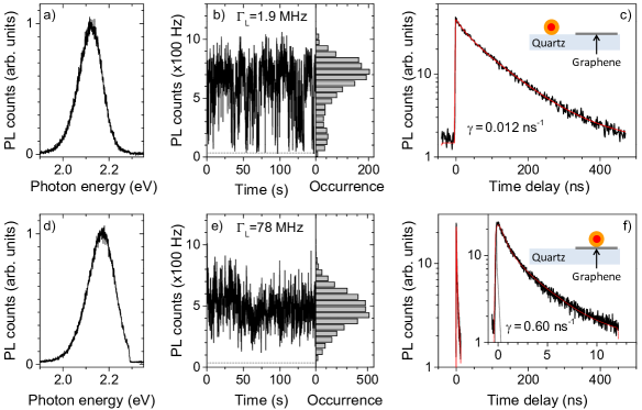
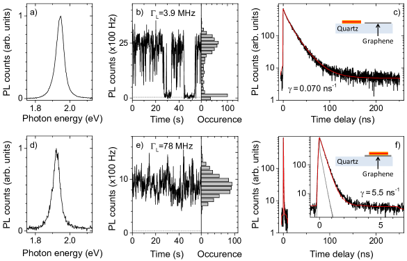
We now compare the PL decays of individual NCs and NPs measured on fused quartz and on graphene. Examples are shown in Figures 2c and 2f for individual NCs and in Figures 3c and 3f, for individual NPs, respectively. At this point, let us note that the room temperature typical PL decay of a single NC or NP is not mono-exponential Spinicelli et al. (2009); Malko et al. (2011); Tessier et al. (2012, 2013). In the case of NCs, we found that most decays could be well fit to a bi-exponential form, while a stretched exponential form was providing better fits in the case of NPs. These complex behaviors are attributed to the existence of a distribution of bright, grey and dark states with distinct lifetimes Cichos et al. (2007); Spinicelli et al. (2009); Malko et al. (2011); Tessier et al. (2012, 2013). The fractional weight of these states in a measured decay may vary significantly from particle to particle, reflecting heterogeneities in core and shell passivation. In order to provide a general definition, the measured PL decay rate is defined as the maximum number of recorded counts divided by the (background corrected) total area of the PL decay. The resulting values are then multiplied by a correction factor, which takes into account the minor contribution of the instrument response function (see Figures 2c,f, Figures 3c,f, and Supporting Information). We have verified that our conclusions are independent of the method used to define the PL decay rate. For the individual NC (NP) considered here, we find that is enhanced by a factor of approximately (). Remarkably, the quenching factors estimated from the PL time traces are in good agreement with the enhancement factors of the PL decay rate. This suggests that the strong PL quenching is solely due to an increase of the non-radiative decay rate, and that possible modifications of the radiative decay rate of an individual NC or NP adsorbed on graphene can be neglected. This is consistent with recent theoretical calculations, which demonstrated that the radiative lifetime of an individual emitter is marginally modified in the vicinity of graphene Gómez-Santos and Stauber (2011). Thus, in the following, we will consider that , where is the RET rate and is the reference decay rate measured in the absence of graphene.
Similar measurements were repeated on more than 100 NCs and NPs deposited on bare graphene. We found similar statistically averaged quenching factors of approximately 50 for NCs and NPs. Overall, for of the investigated single NCs and NPs, the RET efficiency, defined as is found to be larger than .
Distance dependence of the RET rate
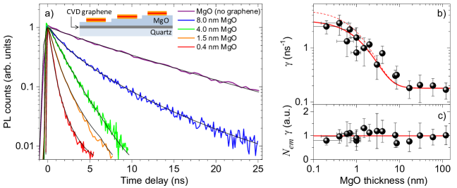
We have measured the PL decay of NCs and NPs separated from a graphene monolayer by a MgO thin film, with a thickness ranging from a few up to several tens of nanometers. In these experiments, the reference decay rate is the statistically averaged decay rate of NCs and NPs measured on a bare thick film of MgO. The results for NCs and NPs are summarized in Figures 4 and 5, respectively. Each point corresponds to a statistical average over to single NCs, and over more than single NPs, respectively. The vertical error bars correspond to the standard deviations, while the horizontal error bars account for the roughness of the MgO film. For both NC and NPs, we observe that the measured decay rate decreases significantly, when increasing the thickness of the MgO film. However, as shown in figures 4c and 5c, the product varies by less than a factor of 2 and, considering the standard deviations associated with each distribution, can be considered as constant. This generalizes the conclusions drawn from the analysis of Figures 2 and 3.
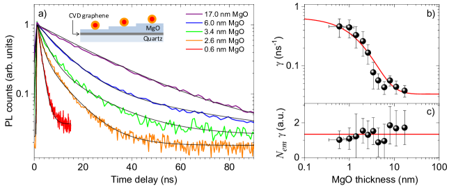
A key observation is that the decrease of the PL decay rate as function of the MgO thickness is seemingly steeper for NCs than for NPs (see also Figure 7 in the Supporting Information for a comparison of the normalized decay rates). This points towards the effect of dimensionality on RET, which we now discuss. Let us first focus on the case of NCs interacting with graphene. Based on the well known distance dependence of the Förster energy transfer rate between two point-like dipoles Förster (1948), one would expect the measured decay rate to scale as
| (1) |
where the distance separating the nanoemitter from the graphene layer is , with , the thickness of the MgO film and , the minimal distance between the center of the nanoemitter and the graphene surface in the absence of a MgO spacer, where characterizes the RET efficiency, and is related to the dimensionality of the donor and acceptor. A straightforward extension of Förster’s theory would then give for a zero-dimensional emitter interacting with a two-dimensional assembly of independent dipoles Kuhn (1970); Chance et al. (1978). Indeed, for NCs (see Fig. 4b, using , we obtain a good fit with and . The latter value is slightly larger than the average physical radius of the NCs, which is consistent with a possible contribution from the surrounding ligands and residual adsorbates to .
Although a fit based on Eq.1 is in good agreement with our measurements, one has to recall that Eq.1 overlooks the fact that graphene is a two-dimensional system with extended, delocalized electronic wavefunctions and a well defined electronic dispersion. The RET rate from a single point-like dipole to graphene has been extensively studied theoretically in recent years Swathi and Sebastian (2008, 2009); Gómez-Santos and Stauber (2011); Velizhanin and Efimov (2011); Gaudreau et al. (2013); Malic et al. (2014) and can be written as Swathi and Sebastian (2009); Gómez-Santos and Stauber (2011)
| (2) |
where is the transferred momentum, is the largest transferable momentum, is the wavelength of the emitted photons, is the speed of light and is the Fermi velocity in graphene. Contrary to far-field emission and absorption processes, the RET process described by Eq.2 involves a finite momentum transfer (see Figure 1a), which is on the order of . For neutral graphene, and distances such that , the denominator of the integrand in Eq.2, which originates from the (momentum dependent) optical conductivity of graphene Gómez-Santos and Stauber (2011), only gives significant contributions for (quasi-vertical transitions), and can thus be approximated as a constant. In these conditions, graphene can be treated as a two-dimensional assembly of incoherent point-like dipoles, and Eq.2 simplifies as . Nevertheless, it must be emphasized that Eq. 2 applies to a point-like donor, while in our case, the NCs have a finite radius, larger than the thinnest MgO films () deposited here. However, the surrounding ligands and the finite thickness of the CdS shell of our CdSe/CdS NCs warrant that there is a minimal distance of a few nanometers between the graphene layer and the emitting CdSe core. We will therefore consider that the long distance approximation is valid and neglect the finite size of the NCs and NPs. Considering random relative dipole orientation, we obtain Swathi and Sebastian (2009) , where is the fine structure constant, is the effective dielectric constant (at ) of the surrounding medium and is a screening factor Califano et al. (2005). Using results in , in good agreement with our measurements.
We now address the distance dependence of the RET rate from single NPs to graphene. The NPs cores are atomically smooth and have recently been shown to behave as genuine quantum wells Ithurria et al. (2011). As a result, a different regime of RET is anticipated when a two-dimensional donor is involved. Electronic states in NPs are described by extended wave functions that are coherent over large distances in the NP plane. However, at finite temperature, one has to consider, in a photoexcited NP, a thermal distribution of excitons with different in-plane center of mass momentum. Besides, since the thickness of the NP shell is on the order of , there is a minimal separation between the NP core and graphene, such that the approximation holds (i.e., graphene can also be treated as an incoherent plane of point-like-dipoles). Similar situations have been previously modeled by Basko et al. Basko et al. (2000) and Kos et al. Kos et al. (2005) for hybrid systems composed of quantum wells transferring energy to an assembly (thick film or monolayer) of point-like dipoles. The calculated RET rate writes
| (3) |
where is the de Broglie thermal length, with the Planck constant, the Boltzmann constant and the mass of the lowest energy heavy hole exciton (, where is the free electron mass) in CdSe Ithurria et al. (2011); Blachnik et al. (1999).
This expression applies to free excitons in an infinite quantum well, with thickness . The assumption of free excitons is consistent with the reported low density of trapping sites of CdSe-based core/shell NPs Tessier et al. (2013). In addition, since the typical lateral dimensions of our NPs ( and ) exceed (at room temperature, ), finite size effects can be neglected. We have thus attempted to fit the data in Figure 5b using the expression . A good agreement with our experimental results is obtained using . Again, the latter value is consistent with the thickness of the core and shell of the NPs and includes a minor contribution from the surrounding ligands and residual adsorbates.
An analysis of the limiting cases of Eq. 3 provides a rationale for the observed scaling. In the short distance limit, , becomes independent on the distance and is determined by the thermal cutoff. In contrast, in the large distance (or high temperature) limit, and follows a scaling, as expected in the case of a two-dimensional assembly of incoherent point-like dipoles. Since, at room temperature, falls exactly in our measurement range, we expect the RET rate to decay more smoothly than for . This is indeed observed experimentally (see Fig 5b), since a scaling based on Eq. 2, with and , having asymptotic behavior for large as our fit based on Eq. 3, would predict a higher in the short distance limit.
The results shown in Figure 5 suggest that even at room temperature, the distance scaling of the RET rate from an extended donor (such as a two-dimensional NP) to graphene exhibits, as expected theoretically, a slight deviation from a simple power law. Following Eq.3, this deviation is expected to be more prominent at lower temperatures. Thus, further investigations of the distance and temperature dependence of the RET rate for various NP architectures could provide insights into the dimensionality of excitons in these novel systems Rindermann et al. (2011).
In conclusion, Förster-type resonant energy transfer dramatically affects the photophysics of semiconductor nanostructures absorbed on graphene. In spite of its atomic thinness, a single layer of graphene typically quenches more than of the luminescence of individual nanocrystals or nanoplatelets. The observation of well-defined distance scalings of the resonant energy transfer rate suggests that novel graphene-based molecular rulers can be engineered using semiconductor nanostructures with different size, shape, and dimensionality. This is a promising development, especially for biological research. Finally, with the prospect of designing hybrid opto-electronic devices, we show that graphene can very efficiently harvest energy from photoexcited semiconductor nanostructures, which is of interest for photodetection. A major challenge is now to dissociate the electron-hole excitations generated in graphene before their fast relaxation into heat Johannsen et al. (2013); Gierz et al. (2013).
Acknowledgement
We are grateful to D.M. Basko and G. Weick for fruitful discussions, to R. Bernard, S. Siegwald and H. Majjad for help with sample fabrication and characterization in the STNano clean room facility, and to M. Romeo for technical support. The authors at IPCMS acknowledge financial support from the CNRS, Université de Strasbourg, C’Nano GE and the Agence Nationale de Recherche (ANR) under grants QuandDoGra ANR-12-JS10-0001 and Fungraph ANR-11-IS10-0003. B.D. (at ESPCI) thanks the ANR for funding under grants SNAP and QDOTICS. J-O. L. (at KRICT) acknowledges support from NRF-ANR program through the National Rearch Foundation of Korea funded by the Ministry of education, Science and Technology (NRF-2011-K2A1A5-2011-0031552).
Supporting Information
Synthesis and characterization of CdSe/CdS nanocrystals and CdSe/CdS/ZnS nanoplatelets, graphene growth by chemical vapor deposition, sample characterization by micro-Raman spectroscopy, definition of the energy transfer rate, comparison of the normalized distance dependent decay rates.
References
- Bonaccorso et al. (2010) F. Bonaccorso, Z. Sun, T. Hasan, and A. C. Ferrari, “Graphene photonics and optoelectronics,” Nature Photonics 4, 611–622 (2010).
- Koppens et al. (2014) F. H. L. Koppens, T. Mueller, Ph Avouris, A. C. Ferrari, M. S. Vitiello, and M. Polini, “Photodetectors based on graphene, other two-dimensional materials and hybrid systems,” Nature Nanotechnology 9, 780–793 (2014).
- Talapin et al. (2010) Dmitri V. Talapin, Jong-Soo Lee, Maksym V. Kovalenko, and Elena V. Shevchenko, “Prospects of colloidal nanocrystals for electronic and optoelectronic applications,” Chemical Reviews 110, 389–458 (2010).
- Nair et al. (2008) R. R. Nair, P. Blake, A. N. Grigorenko, K. S. Novoselov, T. J. Booth, T. Stauber, N. M. R. Peres, and A. K. Geim, “Fine Structure Constant Defines Visual Transparency of Graphene,” Science 320, 1308 (2008).
- Mak et al. (2008) Kin Fai Mak, Matthew Y. Sfeir, Yang Wu, Chun Hung Lui, James A. Misewich, and Tony F. Heinz, “Measurement of the optical conductivity of graphene,” Physical Review Letters 101, 196405 (2008).
- Das Sarma et al. (2011) S. Das Sarma, Shaffique Adam, E. H. Hwang, and Enrico Rossi, “Electronic transport in two-dimensional graphene,” Review of Modern Physics 83, 407–470 (2011).
- Wang et al. (2008a) Xuan Wang, Linjie Zhi, and Klaus Müllen, “Transparent, conductive graphene electrodes for dye-sensitized solar cells,” Nano Letters 8, 323 (2008a).
- Kim et al. (2009a) Keun Soo Kim, Yue Zhao, Houk Jang, Sang Yoon Lee, Jong Min Kim, Kwang S. Kim, Jong-Hyun Ahn, Philip Kim, Jae-Young Choi, and Byung Hee Hong, “Large-scale pattern growth of graphene films for stretchable transparent electrodes,” Nature 457, 706–710 (2009a).
- Edited by Klimov (2010) V.I. Edited by Klimov, Nanocrystal Quantum Dots (CRC Press, UK, 2010).
- Peng et al. (2000) Xiaogang Peng, Liberato Manna, Weidong Yang, Juanita Wickham, Erik Scher, Andreas Kadavanich, and A. P. Alivisatos, “Shape control of CdSe nanocrystals,” Nature 404, 59–61 (2000).
- Ithurria and Dubertret (2008) Sandrine Ithurria and Benoit Dubertret, “Quasi 2D colloidal CdSe platelets with thicknesses controlled at the atomic level,” Journal of the American Chemical Society 130, 16504–16505 (2008).
- Ithurria et al. (2011) S. Ithurria, M. D. Tessier, B. Mahler, R. P. S. M. Lobo, B. Dubertret, and Al L. Efros, “Colloidal nanoplatelets with two-dimensional electronic structure,” Nature Materials 10, 936–941 (2011).
- Chen et al. (2010) Zheyuan Chen, SteÌ?phane Berciaud, Colin Nuckolls, Tony F. Heinz, and Louis E. Brus, “Energy transfer from individual semiconductor nanocrystals to graphene,” ACS Nano 4, 2964–2968 (2010).
- Ajayi et al. (2014) O. A. Ajayi, N. C. Anderson, M. Cotlet, N. Petrone, T. Gu, A. Wolcott, F. Gesuele, J. Hone, J. S. Owen, and C. W. Wong, “Time-resolved energy transfer from single chloride-terminated nanocrystals to graphene,” Applied Physics Letters 104, 171101 (2014).
- Rogez et al. (2014) Benoït Rogez, Heejun Yang, Eric Le Moal, Sandrine Lévêque-Fort, Elizabeth Boer-Duchemin, Fei Yao, Young-Hee Lee, Yang Zhang, K. David Wegner, Niko Hildebrandt, Andrew Mayne, and Gérald Dujardin, “Fluorescence lifetime and blinking of individual semiconductor nanocrystals on graphene,” The Journal of Physical Chemistry C 118, 18445–18452 (2014).
- Konstantatos et al. (2012) Gerasimos Konstantatos, Michela Badioli, Louis Gaudreau, Johann Osmond, Maria Bernechea, F. Pelayo Garcia de Arquer, Fabio Gatti, and Frank H. L. Koppens, “Hybrid graphene-quantum dot phototransistors with ultrahigh gain,” Nature Nanotechnology 7, 363 (2012).
- Sun et al. (2012) Zhenhua Sun, Zhike Liu, Jinhua Li, Guo-an Tai, Shu-Ping Lau, and Feng Yan, “Infrared photodetectors based on cvd-grown graphene and pbs quantum dots with ultrahigh responsivity,” Advanced Materials 24, 5878 (2012).
- Klekachev et al. (2012) Alexander V. Klekachev, Inge Asselberghs, Sergey N. Kuznetsov, Mirco Cantoro, Jeong Hun Mun, Byung-Jin Cho, Jun-ichi Hotta, Johan Hofkens, Marleen van der Veen, André L. Stesmans, Marc M. Heyns, and Stefan De Gendt, “Charge transfer effects in graphene-cdse/zns quantum dots composites,” Proc. SPIE 8462, 84620L (2012).
- Klekachev et al. (2013) Alexander V. Klekachev, Sergey N. Kuznetsov, Inge Asselberghs, Mirco Cantoro, Jeong Hun Mun, Byung Jin Cho, André L. Stesmans, Marc M. Heyns, and Stefan De Gendt, “Graphene as anode electrode for colloidal quantum dots based light emitting diodes,” Applied Physics Letters 103, 043124 (2013).
- Förster (1948) Th Förster, “Zwischenmolekulare energiewanderung und fluoreszenz,” Annalen der physik 437, 55 (1948).
- Velizhanin and Efimov (2011) Kirill A. Velizhanin and Anatoly Efimov, “Probing plasmons in graphene by resonance energy transfer,” Phys. Rev. B 84, 085401 (2011).
- Gómez-Santos and Stauber (2011) G. Gómez-Santos and T. Stauber, “Fluorescence quenching in graphene: A fundamental ruler and evidence for transverse plasmons,” Phys. Rev. B 84, 165438 (2011).
- Tielrooij et al. (2014) K. J. Tielrooij, L. Orona, A. Ferrier, M. Badioli, G. Navickaite, S. Coop, S. Nanot, B. Kalinic, T. Cesca, L. Gaudreau, Q. Ma, A. Centeno, A. Pesquera, A. Zurutuza, H. de Riedmatten, P. Goldner, F. J. Garcia de Abajo, P. Jarillo-Herrero, and F. H. L. Koppens, “Electrical control of optical emitter relaxation pathways enabled by graphene,” arXiv:1410.1361 (2014).
- Lee et al. (2014) Jiye Lee, Wei Bao, Long Ju, P. James Schuck, Feng Wang, and Alexander Weber-Bargioni, “Switching individual quantum dot emission through electrically controlling resonant energy transfer to graphene,” Nano Letters 14, 7115–7119 (2014).
- Shafran et al. (2010) Eyal Shafran, Benjamin D. Mangum, and Jordan M. Gerton, “Energy transfer from an individual quantum dot to a carbon nanotube,” Nano Letters 10, 4049–4054 (2010).
- Jander et al. (2011) Sebastian Jander, Andreas Kornowski, and Horst Weller, “Energy transfer from CdSe/CdS nanorods to amorphous carbon,” Nano Letters 11, 5179–5183 (2011).
- Lin et al. (2013) T. N. Lin, L. T. Huang, G. W. Shu, C. T. Yuan, J. L. Shen, C. A. J. Lin, W. H. Chang, C. H. Chiu, D. W. Lin, C. C. Lin, and H. C. Kuo, “Distance dependence of energy transfer from ingan quantum wells to graphene oxide,” Opt. Lett. 38, 2897–2899 (2013).
- Treossi et al. (2009) Emanuele Treossi, Manuela Melucci, Andrea Liscio, Massimo Gazzano, Paolo Samori, and Vincenzo Palermo, “High-contrast visualization of graphene oxide on dye-sensitized glass, quartz, and silicon by fluorescence quenching,” Journal of the American Chemical Society 131, 15576–15577 (2009).
- Kim et al. (2009b) Jaemyung Kim, Laura J. Cote, Franklin Kim, and Jiaxing Huang, “Visualizing graphene based sheets by fluorescence quenching microscopy,” Journal of the American Chemical Society 132, 260–267 (2009b).
- Gaudreau et al. (2013) L. Gaudreau, K. J. Tielrooij, G. E. D. K. Prawiroatmodjo, J. Osmond, F. J. Garcia de Abajo, and F. H. L. Koppens, “Universal distance-scaling of nonradiative energy transfer to graphene,” Nano Letters 13, 2030–2035 (2013).
- Stöhr et al. (2012) Rainer J. Stöhr, Roman Kolesov, Kangwei Xia, Rolf Reuter, Jan Meijer, Gennady Logvenov, and Jörg Wrachtrup, “Super-resolution fluorescence quenching microscopy of graphene,” ACS Nano 6, 9175–9181 (2012).
- Tisler et al. (2013) Julia Tisler, Thomas Oeckinghaus, Rainer J. Stöhr, Roman Kolesov, Rolf Reuter, Friedemann Reinhard, and Jörg Wrachtrup, “Single defect center scanning near-field optical microscopy on graphene,” Nano Letters 13, 3152–3156 (2013).
- Wang et al. (2011) Ying Wang, Zhaohui Li, Jun Wang, Jinghong Li, and Yuehe Lin, “Graphene and graphene oxide: biofunctionalization and applications in biotechnology,” Trends in Biotechnology 29, 205 – 212 (2011).
- Mazzamuto et al. (2014) G Mazzamuto, A Tabani, S Pazzagli, S Rizvi, A Reserbat-Plantey, K Schädler, G Navickaite, L Gaudreau, F S Cataliotti, F Koppens, and C Toninelli, “Single-molecule study for a graphene-based nano-position sensor,” New Journal of Physics 16, 113007 (2014).
- Halivni et al. (2012) Shira Halivni, Amit Sitt, Ido Hadar, and Uri Banin, “Effect of nanoparticle dimensionality on fluorescence resonance energy transfer in nanoparticle-dye conjugated systems,” ACS Nano 6, 2758–2765 (2012).
- Rindermann et al. (2011) Jan Junis Rindermann, Galia Pozina, Bo Monemar, Lars Hultman, Hiroshi Amano, and Pavlos G. Lagoudakis, “Dependence of resonance energy transfer on exciton dimensionality,” Physical Review Letters 107, 236805 (2011).
- Godel et al. (2013) Florian Godel, Emmanuelle Pichonat, Dominique Vignaud, Hicham Majjad, Dominik Metten, Yves Henry, Stéphane Berciaud, Jean-Francois Dayen, and David Halley, “Epitaxy of MgO magnetic tunnel barriers on epitaxial graphene,” Nanotechnology 24, 475708 (2013).
- Kuhn (1970) Hans Kuhn, “Classical aspects of energy transfer in molecular systems,” The Journal of Chemical Physics 53, 101–108 (1970).
- Chance et al. (1978) R. R. Chance, A. Prock, and R. Silbey, “Molecular fluorescence and energy transfer near interfaces,” Adv. Chem. Phys 37, 65 (1978).
- Swathi and Sebastian (2009) R. S. Swathi and K. L. Sebastian, “Long range resonance energy transfer from a dye molecule to graphene has (distance)−4 dependence,” The Journal of Chemical Physics 130, 086101 (2009).
- Basko et al. (2000) D. M. Basko, V. M. Agranovich, F. Bassani, and G. C. La Rocca, “Energy transfer from a semiconductor quantum dot to an organic matrix,” Eur. Phys. J. B 13, 653–659 (2000).
- Kos et al. (2005) S. Kos, M. Achermann, V. I. Klimov, and D. L. Smith, “Different regimes of förster-type energy transfer between an epitaxial quantum well and a proximal monolayer of semiconductor nanocrystals,” Phys. Rev. B 71, 205309 (2005).
- Mohamed et al. (2005) Mona B. Mohamed, Dino Tonti, Awos Al-Salman, Abdelkrim Chemseddine, and Majed Chergui, “Synthesis of high quality zinc blende cdse nanocrystals,” The Journal of Physical Chemistry B 109, 10533–10537 (2005).
- Mahler et al. (2008) Benoit Mahler, Piernicola Spinicelli, Stéphanie Buil, Xavier Quelin, Jean-Pierre Hermier, and Benoit Dubertret, “Towards non-blinking colloidal quantum dots,” Nature Materials 7, 659–664 (2008).
- Mahler et al. (2012) Benoit Mahler, Brice Nadal, Cecile Bouet, Gilles Patriarche, and Benoit Dubertret, “Core/Shell colloidal semiconductor nanoplatelets,” Journal of the American Chemical Society 134, 18591–18598 (2012).
- Tessier et al. (2013) M. D. Tessier, B. Mahler, B. Nadal, H. Heuclin, S. Pedetti, and B. Dubertret, “Spectroscopy of colloidal semiconductor Core/Shell nanoplatelets with high quantum yield,” Nano Letters 13, 3321–3328 (2013).
- Hines and Guyot-Sionnest (1996) Margaret A. Hines and Philippe Guyot-Sionnest, “Synthesis and characterization of strongly luminescing zns-capped cdse nanocrystals,” The Journal of Physical Chemistry 100, 468–471 (1996).
- Li et al. (2009) Xuesong Li, Weiwei Cai, Jinho An, Seyoung Kim, Junghyo Nah, Dongxing Yang, Richard Piner, Aruna Velamakanni, Inhwa Jung, Emanuel Tutuc, Sanjay K. Banerjee, Luigi Colombo, and Rodney S. Ruoff, “Large-area synthesis of high-quality and uniform graphene films on copper foils,” Science 324, 1312–1314 (2009).
- Wang et al. (2008b) W. H. Wang, W. Han, K. Pi, K. M. McCreary, F. Miao, W. Bao, C. N. Lau, and R. K. Kawakami, “Growth of atomically smooth mgo films on graphene by molecular beam epitaxy,” Applied Physics Letters 93, 183107 (2008b).
- Leatherdale et al. (2002) C. A. Leatherdale, W.-K. Woo, F. V. Mikulec, and M. G. Bawendi, “On the absorption cross section of CdSe nanocrystal quantum dots,” The Journal of Physical Chemistry B 106, 7619–7622 (2002).
- Park et al. (2011) Y.-S. Park, A. V. Malko, J. Vela, Y. Chen, Y. Ghosh, F. Garcia-Santamaria, J. A. Hollingsworth, V. I. Klimov, and H. Htoon, “Near-unity quantum yields of biexciton emission from nanocrystals measured using single-particle spectroscopy,” Physical Review Letters 106, 187401 (2011).
- She et al. (2014) Chunxing She, Igor Fedin, Dmitriy S. Dolzhnikov, Arnaud Demortière, Richard D. Schaller, Matthew Pelton, and Dmitri V. Talapin, “Low-threshold stimulated emission using colloidal quantum wells,” Nano Letters 14, 2772–2777 (2014).
- Cichos et al. (2007) F Cichos, C Vonborczyskowski, and M Orrit, “Power-law intermittency of single emitters,” Current Opinion in Colloid & Interface Science 12, 272–284 (2007).
- Spinicelli et al. (2009) P. Spinicelli, S. Buil, X. Quélin, B. Mahler, B. Dubertret, and J.-P. Hermier, “Bright and grey states in cdse-cds nanocrystals exhibiting strongly reduced blinking,” Physical Review Letters 102, 136801 (2009).
- Malko et al. (2011) Anton V. Malko, Young-Shin Park, Siddharth Sampat, Christophe Galland, Javier Vela, Yongfen Chen, Jennifer A. Hollingsworth, Victor I. Klimov, and Han Htoon, “Pump-intensity- and shell-thickness-dependent evolution of photoluminescence blinking in individual Core/Shell CdSe/CdS nanocrystals,” Nano Letters 11, 5213–5218 (2011).
- Tessier et al. (2012) Mickaël D. Tessier, Clémentine Javaux, Ivan Maksimovic, Vincent Loriette, and Benoit Dubertret, “Spectroscopy of single CdSe nanoplatelets,” ACS Nano 6, 6751–6758 (2012).
- Swathi and Sebastian (2008) R. S. Swathi and K. L. Sebastian, “Resonance energy transfer from a dye molecule to graphene,” The Journal of Chemical Physics 129, 054703 (2008).
- Malic et al. (2014) Ermin Malic, Heiko Appel, Oliver T. Hofmann, and Angel Rubio, “Förster-induced energy transfer in functionalized graphene,” The Journal of Physical Chemistry C 118, 9283–9289 (2014).
- Califano et al. (2005) Marco Califano, Alberto Franceschetti, and Alex Zunger, “Temperature dependence of excitonic radiative decay in CdSe quantum dots: The role of surface hole traps,” Nano Letters 5, 2360–2364 (2005).
- Blachnik et al. (1999) R. Blachnik, J. Chu, R.R. Galazka, J. Geurts, J. Gutowski, B. Hönerlage, D. Hofmann, J. Kossut, R. Lévy, P. Michler, U. Neukirch, T. Story, D. Strauch, and A. Waag, “Semiconductors: Ii-vi and i-vii compounds; semimagnetic compounds,” in Landolt-Börnstein, New Series III/41B, edited by U. Rössler (Springer Verlag, 1999).
- Johannsen et al. (2013) Jens Christian Johannsen, Søren Ulstrup, Federico Cilento, Alberto Crepaldi, Michele Zacchigna, Cephise Cacho, I. C. Edmond Turcu, Emma Springate, Felix Fromm, Christian Raidel, Thomas Seyller, Fulvio Parmigiani, Marco Grioni, and Philip Hofmann, “Direct view of hot carrier dynamics in graphene,” Physical Review Letters 111, 027403 (2013).
- Gierz et al. (2013) Isabella Gierz, Jesse C. Petersen, Matteo Mitrano, Cephise Cacho, I. C. Edmond Turcu, Emma Springate, Alexander Stöhr, Axel Köhler, Ulrich Starke, and Andrea Cavalleri, “Snapshots of non-equilibrium dirac carrier distributions in graphene,” Nature Materials 12, 1119–1124 (2013).
Supporting Information
S1 Synthesis of CdSe/ CdS nanocrystals
Chemicals:
1-Octadecene (ODE, , Aldrich), oleylamine (OLA, , Fluka), oleic acid (OA, , Aldrich), sodium myristate (, Fluka), cadmium oxide (, Aldrich), selenium powder 100 mesh (, Aldrich), sulfur (, Aldrich), trioctylphosphine (TOP, , Cytec) and tetradecylphosphonic acid (TDPA, , PCI synthesis) were used as received.
Precursors preparation:
Cadmium myristate was prepared according to ref. Yang et al. (2005). The solution of cadmium oleate 0.5 M in oleic acid was synthesized by heating g of CdO in 100 mL of oleic acid at under argon until it turned colorless. The solution was then degassed under vacuum at for 1 hour. Sulfur stock solution in ODE (S-ODE M) was prepared by heating 480 mg of sulfur in 150 mL of degassed ODE at until complete dissolution. TOP-Se 1 M in TOP was prepared by dissolving g of Se powder in 200 mL TOP under magnetic stirring overnight in a glove box.
Synthesis of CdSe cores:
CdSe nanocrystals (NCs) were prepared by a procedure slightly modified adapted by Mahler et al. Mahler et al. (2008) from Mohamed et al. Mohamed et al. (2005). A mixture of 2 mL of Cd(oleate)2 (0.5 M) and 3 mL of ODE was degassed under vacuum at during 30 min and heated under argon flow up to . A mixture of mL of TOP-Se 1 M, mL of oleylamine and 1 g of TDPA was heated until complete dissolution then injected and the solution was annealed for 30 seconds at , and then immediately cooled down to room temperature. The solution was washed up with 40 mL of ethanol. The solution was centrifuged at 5500 RPM in order to precipitate the TDPA. The nanocrystals were suspended in 20 mL of toluene, washed again in 20 mL of ethanol, and dispersed in 10 mL of hexane. The nanocrystals obtained with this protocol were around 2 nm diameter, and their approximate concentration was .
Synthesis of CdS shell on the CdSe cores:
For the CdS shell growth on the CdSe cores, a mixture of 3.1 mL of solution of cores dispersed in hexane, 5 mL ODE and 50 mg Cd(myr)2 was degassed under vacuum, at for 30 minutes, and then put under argon flow. The temperature set value was then increased to , and when the temperature reached , 1 mL of OLA was injected, followed by a mixture of 8 mL SODE (0.1 M), 1.6 mL Cd(OA)2 (0.5 M) and 1 mL OLA at an injection rate of first 2 mL/h for 2 mL, then 16 mL/h for the rest of the seringe. Once the injection was finished, a mixture of 0.5 mL OLA and 0.5 mL Cd(OA)2 0.1 M diluted in OA was added, and the solution was annealed for 10 minutes at . The solution was then cooled down to room temperature and the nanocrystals were washed with ethanol, centrifuged and redispersed in 10 mL hexane.
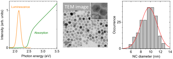
NC characterization:
The ensemble absorption spectrum was measured on a Cary 5E UV-visible spectrometer. The ensemble photoluminescence (PL) spectrum was acquired with an Edinburgh Instruments FCS900 spectrometer. Transmission electron microscopy (TEM) images were taken using a TEM JEOL 2010 with field emission electron gun. The results for CdSe/CdS NCs are shown in Figure S1. The NCs show strong PL at , with a full width at half maximum (FWHM) of . From the analysis of the TEM images, we find an statistically averaged diameter of .
S2 Synthesis of CdSe/CdSeS/ZnS nanoplatelets
Preparation of CdSe nanoplatelets
CdSe nanoplatelets (NPs) with an atomically controlled thickness of 4 monolayers were prepared as described in ref Ithurria and Dubertret (2008). In a 100 mL three neck flask 170 mg (0.3 mmol) of cadmium myristate were introduced along with 12 mg (0.15 mmol) of Se powder and 15 mL of octadecene. The solution was degassed under vacuum for 30 min at room temperature. Under Ar flow, the temperature was set at . When the temperature reached (the solution is yellow orange at this step), 40 mg (0.15 mmol) of cadmium acetate were quickly added to the solution. Finally the reaction was left for 12 min at . Oleic acid (2 mL) were then injected to quench the reaction, and the flask was cooled down to room temperature. The nanoplatelets were precipitated by adding 15 mL of hexane and 15 mL of EtOH. After centrifugation at 6000 rpm for 10 min, the clear supernatant was discarded, and the solid precipitate was re-dissolved in fresh hexane (8 mL). The cleaning procedure was repeated a second time.
Preparation of CdSe/(CdS)3/(ZnS)2 nanoplatelets
CdSe NPs (500 of the solution previously obtained were charged in a 3 mL vial with 0.5 mL of N-methylformamide (NMF) obtaining a biphasic mixture. Then 20 from a freshly solution of Na2S 0.3 M in NMF were added to the biphasic system stirring at room temperature for few minutes. The NPs were thus transferred in the polar NMF bottom phase that turned into orange. The hexane phase was discarded and NPs in NMF were washed twice with hexane to remove residual organic ligand. Then, a mixture of toluene: acetonitrile in a ratio 3:1 is added and NPs were precipitated using centrifugation. The NPs were re-dissolved in 0.5 mL of NMF and 30 of Cd(OAc)2 0.1 M in NMF were added to complete the first CdS monolayer shell deposition. After stirring of few minutes a room temperature, the NPs were precipitated as described above and re-dissolved in 0.5 mL of NMF. The procedure was repeated two more times for a total of 3 CdS layer deposition. To deposit the two final ZnS shell layers, 20 of of Na2S 0.3 M in NMF were added to NPs in NMF and NPs were precipitated using toluene:acetonitrile in a ratio 3:1. After redispersion on NPs in 0.5 mL of NMF, 30 of Zn(OAc)2 0.1 M in NMF were added and the mixture stirred for few minutes at room temperature. Then, it was precipitated as described above and the procedure was repeated once to complete the shell. The final NPs core/shell were precipitated with toluene and redispersed in 1 mL of hexane adding 100 of oleic acid and 50 of oleylamine. The excess of organic ligands was washed away by precipitation with EtOH and finally NPs were dissolved in hexane or toluene to be analyzed by transmission electron microscopy (TEM).
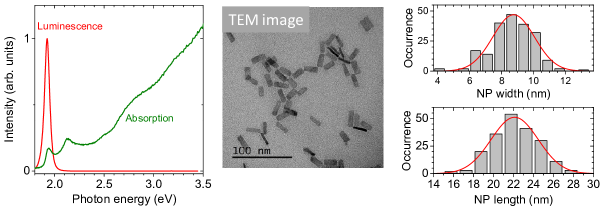
NP characterization:
Optical and TEM characterizations of CdSe/CdS/ZnS NPs used in our measurements were performed using the same instruments as for the CdSe/CdS nanocrystals. Figure S2 shows the absorption and PL spectra, as well as a typical TEM image. These NPs show strong emission at , with a FWHM of . From the analysis of the TEM images, we find an average lateral dimensions of . The average height of the NPs is estimated to be .
S3 Graphene grown by chemical vapor deposition
To investigate the distance scaling of the energy transfer rate we made use of graphene grown by low-pressure chemical vapor deposition (LPCVD) on a Cu foil (Alfa Aesar, Item No. 46986, , cut into 6 x 6 cm strips) in a hot wall furnace consisting of a 4 inch fused silica tube Li et al. (2009). Prior to CVD, the foils were cleaned using a Ni etchant for 5 min and then thoroughly rinsed with DI water. A typical growth process flow is as follows: (1) load the Cu foil, evacuate, heat to , and anneal for 20 min under a 100 sccm H2 flow (at a pressure of about ); (2) introduce 30 sccm CH4 and 30 sccm H2 for 40 min(); (3) final exposure to CH4 for 40 min, followed by a cool down of furnace to room temperature in vacuum. A poly(methyl methacrylate) (PMMA) solution (950 K, by volume dissolved in chlorobenzene) was spin-coated onto the top side of the sample followed by baking at for 5 min. The Cu under the graphene film was etched using a copper etchant solution and washed with DI water 3 times. The resulting PMMA/grapheme film is transferred onto a fused quartz substrate and the PMMA film is dissolved using acetone. In order to remove resist residues and other chemical contaminants from the graphene surface, the samples were heated at for 4 hours in a tube furnace in a Ar/H2 ( mixture composition) atmosphere.
S4 Sample characterization by Raman spectroscopy
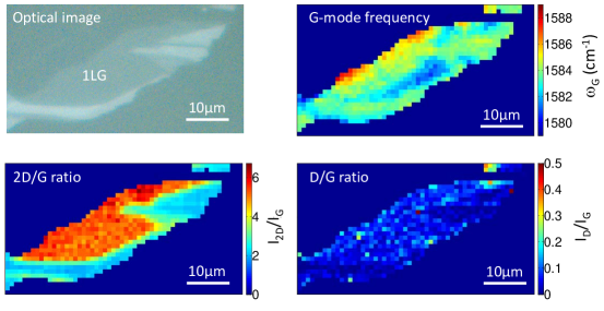
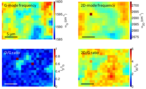
Micro-Raman measurements were performed using a home-built setup, with a laser photon energy of 2.33 eV (532 nm) and a power of a few hundred W focused onto a diffraction limited spot of diameter. Figure S3a shows Raman spectra of a mechanically exfoliated graphene monolayer before and after deposition of a thin MgO layer by means of molecular beam epitaxy Godel et al. (2013). The narrow and quasi symmetric lineshape of the 2D mode feature (frequency , FWHM ) is a fingerprint of a graphene monolayer Ferrari and Basko (2013). The bare graphene monolayer exhibits a G-mode frequency (FWHM) of () that are indicative of a slight unintentional doping, on the order of . This translates into a shift of the Fermi level of less than relative to the Dirac point Das et al. (2008).
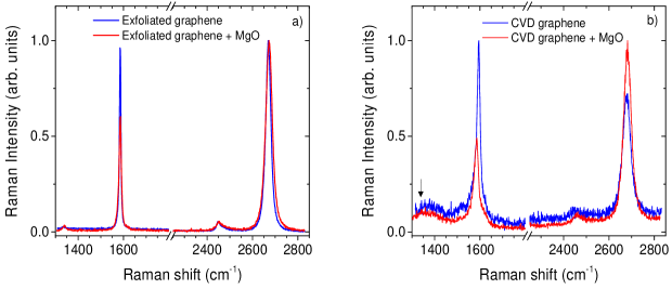
After deposition of MgO, we find very similar G and 2D mode frequencies and a slight broadening of the Raman features. The integrated intensity ratio of the defect-induced D mode and the G mode features increases moderately from up to , but remains low (see also Figure S4. We conclude that the deposition of MgO has no major impact on the doping level and is not introducing significant strain as evidenced by the very slight changes in the frequencies. Similar conclusions are reached for a CVD graphene sample transferred on fused silica (see Figure S3b and Figure S5). We observe a slightly stronger background than for measurements on mechanically exfoliated graphene, presumably arising from PMMA residues. CVD graphene also exhibits broader Raman features, with slightly more scattered frequencies (compare Figure S4 and Figure S5) than for mechanically exfoliated graphene. This likely arises from increased disorder and residual charge inhomogeneity in CVD graphene. Nevertheless, the Raman features are not significantly affected by the deposition of MgO. These results justify the suitability of CVD graphene for our measurements.
S5 Determination of the decay rates
We define the calculated luminescence decay time as the ratio between the area under the background corrected PL decay curve and its peak value. Applying the latter procedure to our instrument response function (IRF) (see Figures 2 and 3 in the main manuscript) yields a value of . Since the shortest values measured for NPs on graphene are below 1 ns, the contribution of the IRF to the PL decay has to be taken into account. For this purpose, we have computed for a set of mono-exponential decays (with a decay time ) that have been convoluted with the IRF. The resulting are plotted against in Figure S6).
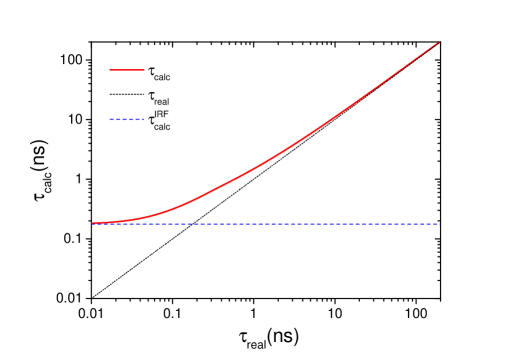
Then, for each measured PL decay, we calculate and estimate a value of , by interpolating the calibration curve shown in Figure S6. Obviously, the obtained correction factor assumes a mono-exponential decay. In practice, since is always significantly greater than , similar correction factors are obtained using other functional forms (bi-exponential decays or stretched exponential decays). We therefore chose to use the procedure described above in order to obtain a general definition of .
In Figures 4 and 5 of the main manuscript, for each thickness of the MgO spacer, we have defined the average decay rate as the inverse of the average decay time . We have verified that our conclusions are independent of the method used to define the average PL decay rate.
S6 Comparison of the distance dependent decay rates
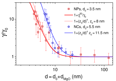
Figure S7 compares the normalized distance decay rates measured for NCs and NPs (see Figures 4 and 5 of the main manuscript) as a function of the total distance between the nanoemitters and graphene. Since the minimal distance (see main text) is smaller for NPs than for NCs, our results suggest that at a given total distance, the RET rate is larger in the case of a zero dimensional NC than for a two-dimensional NP.
References
- Yang et al. (2005) Yongan Andrew Yang, Huimeng Wu, Kathryn R. Williams, and Y. Charles Cao, “Synthesis of cdse and cdte nanocrystals without precursor injection,” Angewandte Chemie International Edition 44, 6712–6715 (2005).
- Mahler et al. (2008) Benoit Mahler, Piernicola Spinicelli, Stéphanie Buil, Xavier Quelin, Jean-Pierre Hermier, and Benoit Dubertret, “Towards non-blinking colloidal quantumdots,” Nature Materials 7, 659–664 (2008).
- Mohamed et al. (2005) Mona B. Mohamed, Dino Tonti, Awos Al-Salman, Abdelkrim Chemseddine, and Majed Chergui, “Synthesis of high quality zinc blende cdse nanocrystals,” The Journal of Physical Chemistry B 109, 10533–10537 (2005).
- Ithurria and Dubertret (2008) Sandrine Ithurria and Benoit Dubertret, “Quasi 2D colloidal CdSe platelets with thicknesses controlled at the atomic level,” Journal of the American Chemical Society 130, 16504–16505 (2008).
- Li et al. (2009) Xuesong Li, Weiwei Cai, Jinho An, Seyoung Kim, Junghyo Nah, Dongxing Yang, Richard Piner, Aruna Velamakanni, Inhwa Jung, Emanuel Tutuc, Sanjay K. Banerjee, Luigi Colombo, and Rodney S. Ruoff, “Large-area synthesis of high-quality and uniform graphene films on copper foils,” Science 324, 1312–1314 (2009).
- Godel et al. (2013) Florian Godel, Emmanuelle Pichonat, Dominique Vignaud, Hicham Majjad, Dominik Metten, Yves Henry, Stéphane Berciaud, Jean-Francois Dayen, and David Halley, “Epitaxy of MgO magnetic tunnel barriers on epitaxial graphene,” Nanotechnology 24, 475708 (2013).
- Ferrari and Basko (2013) Andrea C. Ferrari and Denis M. Basko, “Raman spectroscopy as a versatile tool for studying the properties of graphene,” Nature Nanotechnology 8, 235–246 (2013).
- Das et al. (2008) A. Das, S. Pisana, B. Chakraborty, S. Piscanec, S. K. Saha, U. V. Waghmare, K. S. Novoselov, H. R. Krishnamurthy, A. K. Geim, A. C. Ferrari, and A. K. Sood, “Monitoring dopants by raman scattering in an electrochemically top-gated graphene transistor,” Nature Nanotechnology 3, 210–215 (2008).