Circuit models and SPICE macro-models for quantum Hall effect devices
Abstract
Quantum Hall effect (QHE) devices are a pillar of modern quantum electrical metrology. Electrical networks including one or more QHE elements can be used as quantum resistance and impedance standards. The analysis of these networks allows metrologists to evaluate the effect of the inevitable parasitic parameters on their performance as standards. This paper presents a systematic analysis of the various circuit models for QHE elements proposed in the literature, and the development of a new model. This last model is particularly suited to be employed with the analogue electronic circuit simulator SPICE. The SPICE macro-model and examples of SPICE simulations, validated by comparison with the corresponding analytical solution and/or experimental data, are provided.
1 Introduction
The quantum Hall effect (QHE) has been the basis of resistance metrology for several years in DC [1, 2, 3] and more recently in the AC regime [4, 5, 6, 7]. In DC, networks of several QHE elements have been developed to realize quantum Hall array resistance standards (QHARS) [8, 9, 10, 11, 12, 13, 14, 15, 16], intrinsically-referenced voltage dividers [17] and Wheatstone bridges [18]. In AC, Schurr et al. [19] included two QHE elements in a quadrature bridge to realize the unit of capacitance.
In 1988, Ricketts and Kemeny (RK) [20] proposed a circuit model suitable for the symbolic analysis of arbitrary electrical networks containing QHE elements, in DC or AC. The predictions of the RK model were also verified experimentally [20, 21]. Other circuit models were developed in later years [22, 23, 21, 24, 25, 26, 27, 28] and a general method of analysis based on the indefinite admittance matrix has been recently proposed [29].
The circuit models proposed in the literature are better suited for the symbolic analysis of networks of QHE elements; the matrix method can be employed both for symbolic and numerical analyses, typically with the aid of a computer algebra system or a numerical computing environment. Nowadays, however, the numerical analysis of electrical circuits is commonly carried out by employing analogue electronic circuit simulation tools, like SPICE [30] and its derivatives. SPICE can perform simulations of linear and non-linear networks in time and frequency domains, and noise analysis. Hence, it could be a very useful tool for the simulation of electrical networks containing QHE elements. Unfortunately, even though the above cited circuit models can be directly coded in SPICE, several issues arise when trying to run a simulation. The aim of this work is to address these issues and to present a working SPICE macro-model for the simulation of networks of QHE elements.
In section 2, we review the existing circuit models for QHE elements and present a new one. In section 3, we discuss the issues of SPICE modelling and provide a SPICE macro-model for an 8-terminal QHE element, which is based on the new circuit model. In section 4, three simulation examples are worked out in detail: i) a DC analysis taking into account parasitic resistances; ii) an AC analysis of a network containing a QHE element and a capacitor; iii) a noise analysis. The simulation of example i) is compared with an analytical result; those of ii) and iii) are compared with analytical and experimental results. A reports the full derivation of the new circuit model.
2 Brief review of QHE circuit models
The development of circuit models for the Hall effect is not a recent topic. For models related to the classical Hall effect see, e.g.,[31, 32, 33, 34, 35]; in this section, instead, we shall briefly review the existing circuit models for ideal QHE elements.
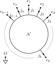
In circuit theory, an -terminal element is a black-box which can interact with its surroundings solely through conductors called terminals (figure 1). A basic assumption of circuit theory is that an -terminal element is completely characterized by its external behaviour, that is, by the set of admissible terminal voltage-current pairs (action at distance is excluded) [36, 37]. Two elements are thus equivalent from the point of view of circuit theory if they have the same external behaviour.
An electric circuit composed of several interconnected elements can be itself turned into an -terminal element by connecting terminals to selected nodes of the circuit. If a circuit, viewed as an -terminal element, is equivalent to a certain -terminal element , it is called a circuit model (or equivalent circuit) for .
According to their external behaviour, ideal QHE elements can be classified in two categories. In the following, we shall call111The terminology has been inspired by the two circuit models shown in the first row of table 1. an ideal clockwise (cw) -terminal QHE element with Hall resistance , an element whose terminal voltages and currents are related by the equations
| (1) |
with the convention , and we shall call an ideal counterclockwise (ccw) -terminal QHE element, an element whose terminal voltages and currents are related by the equations
| (2) |
with the convention . Ideal QHE elements are memoryless, passive (actually, they dissipate power) and nonreciprocal222They are memoryless because the sets of equations (1) and (2) relate terminal voltages and currents at the same time instant. For definitions of passivity and reciprocity see e.g. [38, Ch. 2]..
The sets of equations (1) and (2) are, indeed, a consequence of the QHE phenomenology, but can also be derived theoretically on the basis of the Landauer-Büttiker formalism (see, e.g., [39, Sec. 16.3] and references therein).
A real QHE device operating at appropriate values of temperature and magnetic flux density can be modelled, with a certain approximation, either as an ideal cw or an ideal ccw element depending on the orientation of the magnetic field applied to the device and on the type of the majority charge carriers. The Hall resistance is quantized, , where is the von Klitzing constant and is a positive integer called plateau index. In QHE devices realized with GaAs technology, the plateau index of interest for resistance metrology is , so . The recommended value of the von Klitzing constant is , which yields [40]. The conventional value adopted internationally for resistance metrology is , which yields . In section 4, we shall use this last value for the Hall resistance of the QHE elements in the example circuits.
| Reference | 4-terminal cw model | 4-terminal ccw model | Outline of the 6-terminal model (cw) |
|---|---|---|---|
| 1. Ricketts-Kemeny [20] |
![[Uncaptioned image]](/html/1501.03288/assets/x2.png)
|
![[Uncaptioned image]](/html/1501.03288/assets/x3.png)
|
|
| 2. Hartland et al. [22, 23] |
![[Uncaptioned image]](/html/1501.03288/assets/x5.png)
|
![[Uncaptioned image]](/html/1501.03288/assets/x6.png)
|
No generalization has been directly proposed by the authors |
| 3. Jeffery et al. [21, 24] |
![[Uncaptioned image]](/html/1501.03288/assets/x7.png)
|
![[Uncaptioned image]](/html/1501.03288/assets/x8.png)
|
|
| 4. Sosso-Capra [25, 26] |
![[Uncaptioned image]](/html/1501.03288/assets/x10.png)
|
![[Uncaptioned image]](/html/1501.03288/assets/x11.png)
|
![[Uncaptioned image]](/html/1501.03288/assets/x12.png)
|
| 5. Schurr et al. [27, 28] |
![[Uncaptioned image]](/html/1501.03288/assets/x13.png)
|
![[Uncaptioned image]](/html/1501.03288/assets/x14.png)
|
|
| 6. This work (A) |
![[Uncaptioned image]](/html/1501.03288/assets/x16.png)
|
![[Uncaptioned image]](/html/1501.03288/assets/x17.png)
|
|
Table 1 reports known circuit models listed in order of appearance in the literature: the first row reports the well-known circuit of Ricketts and Kemeny [20]; the last one, a new circuit model whose derivation is given in A. For each referenced work, the second and third columns show the circuit models corresponding to the ideal cw and ccw 4-terminal QHE elements (the cited works might not provide both); in order to see how these models can be extended to elements with more than 4 terminals, the fourth column shows the outlines of the circuit models corresponding to a cw 6-terminal element. All circuit models contain only resistors (because of memorylessness and passivity) and controlled sources (because of nonreciprocity); none of them are related to the actual device physics.
We remark that the sets of equations (1) and (2) are all that is needed to analyse circuits containing ideal QHE elements [29], and that the external behaviour of all the models listed in table 1 is exactly described by those equations. Nonetheless, a circuit model can be a useful basis for taking into account nonidealities (e.g. nonzero longitudinal resistances [24, 27], parasitic elements in AC regime [41]) or to develop a SPICE macro-model, as we shall see in the next section.
3 SPICE modelling
In SPICE a circuit is represented by a list of statements (netlist), written according to a certain specific syntax [30, 42], which describes how the elements that compose the circuit are interconnected. A SPICE macro-model (or subcircuit netlist) is a netlist with a designated name that can be treated as any other SPICE element to compose larger circuits in a hierarchical way. Circuits composed exclusively of resistors and controlled sources can be directly translated into SPICE macro-models. Given that all the models reported in table 1 are equivalent from the point of view of circuit theory, and that many more possessing this property can be conceived, how can we select one with the purpose of writing a SPICE macro-model?
In reality, SPICE modelling requires at least two additional properties, (1) and (2) below, but one more, (3), would be useful:
-
1.
No loops of voltage sources. SPICE requires a circuit that does not contain loops composed only of ideal voltage sources (independent or controlled). In fact, violating this requirement would lead to two scenarios: either Kirchhoff’s voltage law would be violated or the current crossing the loop would be indeterminate and the circuit would not have a unique solution. In both cases, SPICE would not be able to solve the circuit.
-
2.
No cut sets of current sources. This property is the dual of (1). If, in a circuit, there is a node where only current sources join, either Kirchhoff’s current law would be violated or the node potential would be indeterminate (floating node).
-
3.
Non-dissipative/generative sources. As stated in section 2, QHE elements are passive elements that dissipate power. One property that could then be required by the circuit model is that all the power is dissipated in the resistors and that the overall power absorbed or delivered by the controlled sources is zero. This property would also allow SPICE to predict the thermal noise generated by the QHE elements correctly (see A for more details on this). Even though this property is not strictly required, and even though SPICE has a few limitations in noise analysis (e.g. it is not able to analyse correlations directly and a workaround is needed [43]), it might be useful to have a circuit model which is as complete as possible.
By inspection, it is easy to verify that models 1 and 3 of table 1 violate property (1) and that model 6 violates property (2); property (1) can also be violated by model 5 if a voltage source is connected between terminals 1 and 2, or 3 and 4. In addition, it is straightforward to verify that models 2,4 and 5 violate property (3)333For instance, for model 5 (cw), the power delivered by the controlled sources is , which is generally not zero..
Models 2,4 and 5 cannot be easily modified to satisfy property (3) and will not be considered further. Models 1 and 3 can be modified to satisfy property (1) either by adding a small series resistance to the loop of voltage sources [44] or by removing one of the controlled sources in the loop (this does not alter the model’s behaviour). However, none of the above two remedies is completely satisfactory: the former because the effect of the additional resistance on the simulation accuracy cannot be easily predicted in the case of many interconnected QHE elements; the latter because it destroys the symmetry of the model, making it more difficult to develop possible refinements to take account of nonidealities. For model 6, it is worth noting that the potential of the floating node can be fixed arbitrarily without altering the model’s behaviour; this allows the satisfaction of property (2) without the need for additional elements and without destroying the circuit symmetry. Therefore, model 6 was selected to implement a SPICE macro-model.
Listings 1 and 2 report, respectively, the SPICE macro-models for ideal cw and ccw 8-terminal QHE elements444These macro-models should work out of the box, or with just slight modifications, with any modern SPICE simulator that accepts subcircuits with parameters. In this work, we have chiefly used LTspice IV from Linear Technology Corporation [45], but tests have been carried out also with the open source simulator Ngspice [46], with PSpice A/D from Cadence Design Systems and with TINA-TI from Texas Instruments. The authors can provide advice on adapting the circuit models and the simulations here described to other SPICE-based analogue circuit simulators.. These macro-models are a direct translation of the general circuit models derived in A. The actual number of terminals is nine: the ninth terminal, labelled C, corresponds to the node joining the controlled current sources and has to be connected to an arbitrary potential (e.g. ground). The default value of is , but other values can be assigned when calling the macro-model (see next section for an example).
4 Examples
4.1 Double-series interconnection of two QHE elements
Several QHE elements can be interconnected to obtain multiples, submultiples or fractions of the Hall resistance. Multiple-series, parallel[47] and bridge connections [48] can be employed to reject the effect of the inevitable contact and wiring resistances. In this section, SPICE is used to analyse, in the DC regime, the effect of the parasitic resistances in a double-series connection; the result of the SPICE analysis is then compared with an analytical solution obtained with the technique described in [29].
Figure 2 shows the complete circuit diagram for the analysis of the double-series connection. For ease of analysis, only two parasitic resistances, and (), are taken into account. The resistance of the double-series is calculated between the terminal 1a and ground, , where can be chosen of to simplify the calculation. The effect of the parasitic resistances can be quantified by the relative discrepancy
| (3) |
where is the resistance of the double-series when . At the third order in and , the analytical solution yields555The authors can provide the Mathematica® notebook used to obtain the analytical solution.
| (4) |
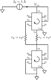
The SPICE netlist666Modern SPICE simulators come with handy graphical schematic editors which alleviate the chore of writing netlists. Here, however, we have preferred to provide netlists, using basic elements and directives, which can be easily converted from one SPICE dialect to another (the dialect employed here is mainly that of LTspice IV). which corresponds to the circuit of figure 2 is reported in listing 3, with example parasitic resistances and , where we have introduced a scaling parameter to check the round-off errors due to floating point arithmetic and numerical algorithms. From (3), is expected to scale as .
Table 2 reports a comparison, for different values of , between the values of obtained from (3) and those of obtained from the SPICE simulation of listing 3. The third column of table 2 can be considered representative of the results obtainable with common SPICE simulators: as can be seen from the reported results, when falls below , diverges from . The last column (alt) reports, instead, the results obtained with the LTspice IV’s alternate solver, which, according to the LTspice IV manual, has reduced round-off errors. In any case, whatever the simulator employed in this kind of analysis, we suggest to write all parasitic resistances as functions of a scaling parameter to keep under control round-off errors.
| (alt) | |||
|---|---|---|---|
4.2 QHE gyrator
QHE elements, like their classical counterparts, can be employed as gyrators [49, 50]. At the angular frequency , the circuit of figure 3, which includes the load capacitor with negative reactance , realizes between terminal 1 and ground an impedance having positive reactance, that is, for any . Therefore, at any given frequency, the circuit of figure 3 behaves like an two-terminal element (the values of and are frequency-dependent).
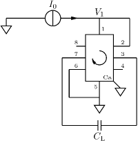
Network analysis yields
| (5) |
for which .
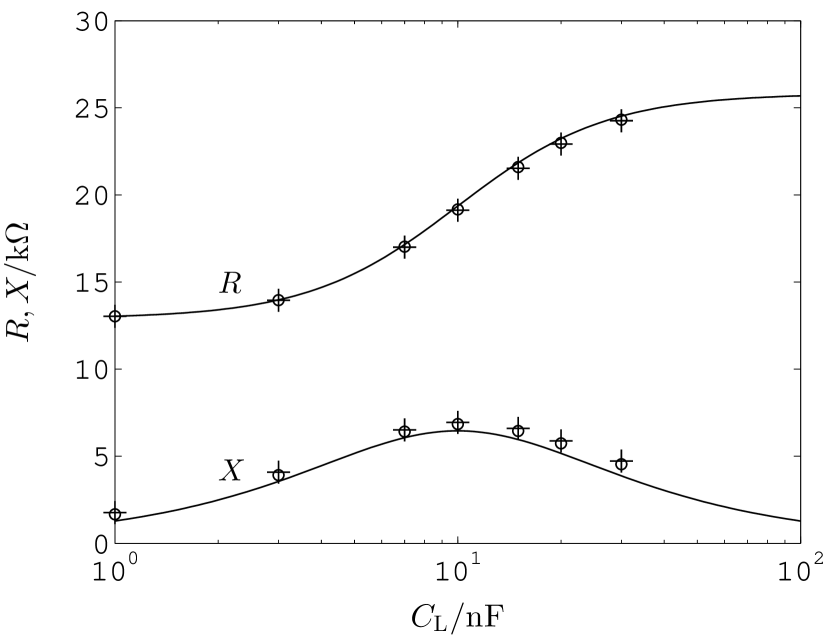
The behaviour of such an unconventional QHE circuit was checked experimentally with an 8-terminal GaAs-AlGaAs Hall bar working at the temperature and plateau index . Terminals 3 and 7 were connected to a variable capacitance box; terminals pairs and were connected in double-series configuration to an LCR meter (Agilent mod. 4284A) which performed the impedance measurements. The measurement frequency was chosen at , so that the reactance of a capacitor is .
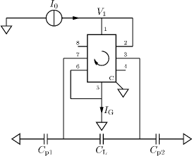
However, the above described experimental set-up is not accurately modelled by the circuit of figure 3 and by the corresponding equation (5), because in figure 3 the cable capacitances and the real operation of the LCR meter are not taken into account (see [7] for an example about the effect of the cable capacitances in AC QHE measurements). The experimental set-up is instead better modelled by the circuit of figure 4, where and represent the cable capacitances, and where the transimpedance represents the impedance actually measured by the LCR meter, that is, the ratio of the meter’s high-side voltage to the meter’s low-side current.
Even though the circuit of figure 4 can be solved analytically, this kind of analysis is not straightforward, and SPICE simulation can provide a quicker response. Listing 4 reports the SPICE netlist for the AC analysis of the circuit of figure 4, for different values of at the fixed frequency of . The given values for are those used in the experiment: . The values of the parasitic capacitances reported in the listing, , are just rough estimates and not the result of a measurement.
Results are reported in figure 5, where the measured values of and at the frequency of are compared with the values obtained from the SPICE simulation of listing 4 and with those obtained from (5). The agreement between the measured values and those obtained from the SPICE simulation is within . Further model refinements can be easily implemented in the SPICE simulation.
4.3 Noise analysis
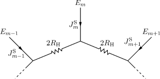
Noise is a fundamental limit to the resolution of a measuring system. Noise analysis is therefore a useful tool to predict the resolution achievable in a measurement. SPICE has built-in noise models for resistors and semiconductor devices which allow a complete noise analysis of circuits, taking into account all the main noise sources. In the case of circuits containing QHE elements, the noise analysis can include the thermal noise generated by these elements and the noise generated by possible auxiliary elements, such as voltage or current sources, detectors etc.
In this section we present the noise analysis of the circuit of figure 6, for which the thermal noise properties have been investigated both theoretically and experimentally in [51]. The one-sided cross-spectral density function between the voltages and due to thermal noise is [51], where is the Boltzmann’s constant and is the thermodynamic temperature of the QHE element.
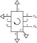
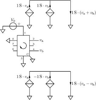
Figure 7 shows the circuit needed to evaluate with SPICE. Since SPICE cannot evaluate directly cross-spectral density functions, but only (auto-) spectral density functions, a trick should be employed [43]. Four voltage controlled current sources, with transconductances of , generate two currents, one proportional to the sum of and , the other proportional to their difference; it can be shown that
| (6) |
where is the spectral density function of and is the spectral density function of . Both and can be directly evaluated by SPICE. The additional, noiseless, voltage source is actually ineffective in this analysis, but it is required by SPICE to have a fictitious input.
Listing 5 reports the SPICE netlist for the noise analysis described above. The subcircuit probe_correlation is used to calculate the sum and the difference of and in two successive steps: when the parameter gb is set to 1 the output node (OUT) of probe_correlation yields the sum of the two voltages; when gb is set to -1, the difference is instead obtained. The simulation temperature is set to . The calculation of or of the ratio can be done automatically by the SPICE graphical post-processor, but we shall not dwell on the details here. The result obtained from the simulation coincides with the theoretical one.
5 Conclusions
In this paper we reviewed the modelling of the ideal quantum Hall effect element as a -terminal electrical network. The unique set of network equations can be represented with different equivalent circuit models published in literature. An analysis of these models shows that they are unsuitable to be directly coded in circuit simulation software such as SPICE, because they generate singular representations or because of errors in the noise simulation. A new QHE circuit model, specifically designed to be implemented in SPICE, is proposed. This paper provides several examples of electrical circuits including QHE elements, of their coding in SPICE and hints for proper simulation runs. For each case, the simulation outcome is compared with the results from analytical modelling and also, in two cases, with experimental data.
Acknowledgments
The authors are grateful to Franz Josef Ahlers and Jürgen Schurr from the Physikalisch-Technische Bundesanstalt (PTB), Braunschweig (Germany), for their collaboration in the experiment described in section 4.2, which was carried out at the Electrical Quantum Metrology Department of the PTB.
The authors would also like to thank Helmut Sennewald and the LTspice IV users’ group [52] for useful suggestions on the usage of LTspice IV.
Appendix A Yet another model
A.1 Model derivation
In this section we derive model 6 of table 1 for an ideal -terminal QHE element on the basis of the analysis method described in [29] and briefly reviewed below. In the derivation, sinusoidal regime is assumed: voltages and currents are to be understood as voltage and current phasors and are denoted with capital letters. Labelling of terminals and reference directions are again that of figure 1.
The sets of equations (1) and (2) can be rewritten in matrix form as [29]
| (7) |
where (the superscript T denotes transposition) and are column vectors, and where the indefinite admittance matrix (see [53] for a definition) is either
| (8) |
in the case of an ideal cw -terminal element, or
| (9) |
in the case of an ideal ccw -terminal element.
The two above matrices are real matrices. A basic theorem of algebra [54, Ch. 1] states that every matrix can be decomposed into the sum of a symmetric part and an antisymmetric one:
| (10) |
with
| (11) |
Since, by definition, , the matrix is associated to a reciprocal network [55, Ch. 16]; in addition, this associated network can be realized with just resistors because is also real. The antisymmetric part is instead associated to a nonreciprocal network that can be realized with voltage controlled current sources. For the matrices in (8) and (9) the symmetric and antisymmetric parts are
| (17) | |||||
| (18) |
and
| (24) | |||||
From (7), taking into account (10), we obtain that the terminal currents can be decomposed into the sum of two contributions, one associated to and one to :
| (25) |
with
| (26) |
This means that and can be considered associated to two electrical networks connected in parallel.
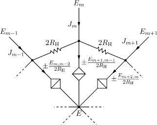
Let : from (26) and (17) the current at the th terminal is (; and )
| (27) | |||||
| (28) |
The last equation above corresponds to a network where each terminal is connected to its adjacent terminals through a resistor with resistance , as shown in figure 8. This can also be obtained directly from the properties of the indefinite admittance matrices [56, Ch. 2, Sec. 2.2].
Now, let : from (26), (18) and (24), the current at the th terminal is
| (29) |
where the plus sign holds for a cw element and the minus for a ccw one. This equation can be obtained with a voltage controlled current source, driven by the voltage difference , which draws from the th terminal the current injecting it into an additional internal node (figure 9).
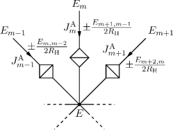
Finally, combining in parallel the two networks, one obtains the circuit model of figure 10. This circuit model obviously satisfies property (1); property (2) can be satisfied by fixing the potential of the central node of figure 10 to an arbitrary value.
A.2 Power
To prove that the circuit model of figure 10 satisfies property (3), let us recall that, in sinusoidal regime, the average power entering an -terminal element is given by [53, 55]
| (30) | |||||
| (31) |
where the operator denotes the real part and the asterisk denotes the conjugate transpose. Substituting (7) in (31), and taking into account that is real, yields
| (32) | |||||
| (33) | |||||
| (34) |
Equation (34) says that the power dissipated in the ideal QHE element is related only to the symmetric part of the corresponding indefinite admittance matrix. Thus, no power is delivered or absorbed by the circuit associated with the antisymmetric part, and property (3) is satisfied.
A.3 Noise modelling
When SPICE performs the noise analysis of a circuit, it automatically assigns noise sources to certain circuit elements, in accordance with known noise models. The insertion of arbitrary noise sources is not permitted. In the case of the macro-models of listings 1 and 2, SPICE will assign noise sources to the resistors only: the controlled sources are considered noiseless. To each resistor, SPICE assign a noise source which generates the corresponding thermal (equilibrium) noise at the simulation temperature (specified by the SPICE parameter TNOM, by default). Therefore, to prove that the satisfaction of property (3) allows SPICE to predict the equilibrium noise generated by the QHE elements correctly, we need only to prove that the equilibrium noise of a QHE element coincides with that of the resistive network associated with .
The equilibrium noise properties of a general passive multiterminal network were derived by Twiss [57] from thermodynamic considerations. Later, Büttiker derived an equivalent result for multiterminal conductors from a quantum scattering theory [58, 59]777The two approaches are complementary: the derivation of Twiss can be considered analogous to that of Nyquist [60] for the Johnson-Nyquist noise generated by a resistor; the derivation of Büttiker can be considered analogous to that of Landauer [61].. These results were verified experimentally by the authors in [51].
For the present purposes, the result given by Twiss is in a more convenient form. This result can be stated as follows [57]: consider a passive -terminal element and assume that all the terminals are grounded and one, say terminal without loss of generality, is considered as reference; then, the one-sided cross-spectral density function [62] between the noise currents and at the terminals and is given by
| (35) |
where is the Boltzmann’s constant, is the thermodynamic temperature and is the short-circuit admittance matrix obtained by considering the -terminal element as an -port with ports defined between the terminals and the reference node .
The short-circuit admittance matrix can be obtained by the indefinite admittance matrix associated to the -terminal element by deleting the th row and column [53]; then, for and ideal QHE element, and
| (36) | |||||
| (37) | |||||
| (38) | |||||
| (39) | |||||
| (40) |
Hence, and taking into account that the reference node is arbitrary, the equilibrium noise of a QHE element coincides with that of the resistive network associated with .
References
References
- [1] Delahaye F and Jeckelmann B 2003 Metrologia 40 217
- [2] Jeckelmann B and Jeanneret B 2003 Meas. Sci. Technol. 14 1229
- [3] Poirier W, Schopfer F, Guignard J, Thévenot O and Gournay P 2011 C. R. Phys. 12 347–368
- [4] Overney F, Jeanneret B, Jeckelmann B, Wood B M and Schurr J 2006 Metrologia 43 409
- [5] Schurr J, Ahlers F J, Hein G and Pierz K 2007 Metrologia 44 15–23
- [6] Ahlers F J, Jeanneret B, Overney F, Schurr J and Wood B M 2009 Metrologia 46 R1–R12
- [7] Hernandez C, Consejo C, Degiovanni P and Chaubet C 2014 J. Appl. Phys. 115 123710
- [8] Piquemal F P M, Blanchet J, Gèneves G and André J P 1999 IEEE Trans. Instr. Meas. 48 296–300
- [9] Poirier W, Bounouh A, Hayashi H, Fhima H, Piquemal F, Gèneves G and André J P 2002 J. Appl. Phys. 92 2844–2854
- [10] Bounouh A, Poirier W, Piquemal F, Gèneves G and André J P 2003 IEEE Trans. Instr. Meas. 52 555–558
- [11] Poirier W, Bounouh A, Piquemal F and André J P 2004 Metrologia 41 285
- [12] Hein G, Schumacher B and Ahlers F J 2004 Preparation of quantum Hall effect device arrays 2004 Conference on Precision Electromagnetic Measurements Digest (London, UK) pp 273–274
- [13] Oe T, Kaneko N, Urano C, Itatani T, Ishii H and Kiryu S 2008 Development of quantum Hall array resistance standards at NMIJ Precision Electromagnetic Measurements Digest, 2008. CPEM 2008. Conf. on (Broomfield, CO, USA) pp 20–21
- [14] Oe T, Matsuhiro K, Itatani T, Gorwadkar S, Kiryu S and Kaneko N 2011 IEEE Trans. Instr. Meas. 60 2590–2595
- [15] Woszczyna M, Friedemann M, Dziomba T, Weimann T and Ahlers F J 2011 Appl. Phys. Lett 99 022112 (pages 3)
- [16] Oe T, Matsuhiro K, Itatani T, Gorwadkar S, Kiryu S and Kaneko N 2013 IEEE Trans. Instr. Meas. 62 1755–1759
- [17] Domae A, Oe T, Matsuhiro K, Kiryu S and Kaneko N 2012 Meas. Sci. Technol. 23 124008
- [18] Schopfer F and Poirier W 2007 J. Appl. Phys. 102 054903
- [19] Schurr J, Bürkel V and Kibble B P 2009 Metrologia 46 619
- [20] Ricketts B W and Kemeny P C 1988 J. Phys. D: Appl. Phys. 21 483
- [21] Jeffery A, Elmquist R and Cage M 1995 J. Res. Natl. Inst. Stan. 100 677–685
- [22] Hartland A, Kibble B, Rodgers P and Bohacek J 1995 IEEE Trans. Instr. Meas. 44 245 –248
- [23] Chua S W, Hartland A and Kibble B 1999 IEEE Trans. Instr. Meas. 48 309 –313
- [24] Cage M, Jeffery A, Elmquist R and Lee K 1998 J. Res. Natl. Inst. Stan. 103 561–592
- [25] Sosso A and Capra P P 1999 Rev. Sci. Instrum. 70 2082–2086
- [26] Sosso A 2001 IEEE Trans. Instr. Meas. 50 223–226
- [27] Schurr J, Ahlers F J, Hein G, Melcher J, Pierz K, Overney F and Wood B M 2006 Metrologia 43 163 URL http://stacks.iop.org/0026-1394/43/i=1/a=021
- [28] Schurr J, Ahlers F and Pierz K 2014 Metrologia 51 235–242
- [29] Ortolano M and Callegaro L 2012 Metrologia 49 1
- [30] The SPICE page Online URL http://bwrcs.eecs.berkeley.edu/Classes/IcBook/SPICE/
- [31] Garg J M and Carlin H J 1965 IEEE Trans. Circuit Theory 59–73
- [32] Arnold E 1982 Surf. Sci. 113 239–243 ISSN 0039-6028 URL http://www.sciencedirect.com/science/article/pii/0039602882905921
- [33] Popović R S 1985 Solid-St. Electron. 28 711–716 ISSN 0038-1101 URL http://www.sciencedirect.com/science/article/pii/0038110185900218
- [34] Salim A, Manku T, Nathan A and Kung W 1992 Modeling of magnetic-field sensitive devices using circuit simulation tools Technical Digest of the 5th IEEE Solid-State Sensor and Actuator Workshop pp 94–97
- [35] Salim A, Manku T and Nathan A 1995 IEEE Trans. Comput.-Aided Design Integr. Circuits Syst. 14 464–469 ISSN 0278-0070
- [36] Chua L O 1980 IEEE Tran. Circuits Syst. 27 1014–1044
- [37] Willems J C 2010 IEEE Circuits Syst. Mag. 10 8–16
- [38] Belevitch V 1968 Classical network theory (San Francisco, CA, USA: Holden-Day)
- [39] Ihn T 2010 Semiconductor Nanostructures: Quantum States and Electronic Transport (Oxford University Press)
- [40] Mohr P J, Taylor B N and Newell D B 2012 Rev. Mod. Phys. 84 1527–1605
- [41] Cage M E, Jeffery A and Matthews J 1999 J. Res. Natl. Inst. Stan. 104 529–556
- [42] Steer M B 2007 SPICE: User’s guide and reference Online URL http://www.freeda.org/doc/SPICE/spice.pdf
- [43] McAndrew C, Coram G, Blaum A and Pilloud O 2005 Correlated noise modeling and simulation Technical Proceedings of the 2005 Workshop on Compact Modeling (Anaheim, CA, US) pp 40–45
- [44] Rashid M H and Rashid H M 2006 SPICE for Power Electronics and Electric Power 2nd ed (Boca Raton, FL, USA: CRC Press)
- [45] Linear Technology LTspice IV URL http://www.linear.com/designtools/software/
- [46] Ngspice home page URL http://ngspice.sourceforge.net/
- [47] Delahaye F 1993 J. Appl. Phys. 73 7914–7920
- [48] Ortolano M, Abrate M and Callegaro L 2015 Metrologia 52 31
- [49] Tellegen B D H 1948 Philips Res. Rept. 3 81–101
- [50] Viola G and DiVincenzo D P 2014 Phys. Rev. X 4 021019
- [51] Callegaro L, Ortolano M and Schurr J 2013 Europhys. Lett. 101 50003
- [52] LTspice IV users’ group URL http://groups.yahoo.com/group/LTspice
- [53] Shekel J 1954 Wireless Engineer 31 6–10
- [54] Roman S 2010 Advanced Linear Algebra 3rd ed (Springer)
- [55] Desoer C A and Kuh E S 1969 Basic circuit theory (Singapore: McGraw-Hill, Inc.)
- [56] Chen W 1991 Active network analysis (Singapore: World Scientific Publishing Co.)
- [57] Twiss R Q 1955 J. Appl. Phys. 26 599–602
- [58] Büttiker M 1990 Phys. Rev. Lett. 65(23) 2901–2904 URL http://link.aps.org/doi/10.1103/PhysRevLett.65.2901
- [59] Büttiker M 1992 Phys. Rev. B 46(19) 12485–12507 URL http://link.aps.org/doi/10.1103/PhysRevB.46.12485
- [60] Nyquist H 1928 Phys. Rev. 32(1) 110–113
- [61] Landauer R 1989 Physica D 38 226–229
- [62] Priestley M B 1981 Spectral analysis and time series vol 2 (Academic Press)