Controlling the Schottky barrier at MoS2metal contacts by inserting a BN monolayer
Abstract
Making a metal contact to the two-dimensional semiconductor MoS2 without creating a Schottky barrier is a challenge. Using density functional calculations we show that, although the Schottky barrier for electrons obeys the Schottky-Mott rule for high work function ( eV) metals, the Fermi level is pinned at 0.1-0.3 eV below the conduction band edge of MoS2 for low work function metals, due to the metal-MoS2 interaction. Inserting a boron nitride (BN) monolayer between the metal and the MoS2 disrupts this interaction, and restores the MoS2 electronic structure. Moreover, a BN layer decreases the metal work function of Co and Ni by eV, and enables a line-up of the Fermi level with the MoS2 conduction band. Surface modification by adsorbing a single BN layer is a practical method to attain vanishing Schottky barrier heights.
pacs:
73.30.+y, 73.20.At, 79.60.JvIntroduction. Single layers of transition metal dichalcogenides (TMDs) such as molybdenite, MoS2, can be exfoliated through micromechanical cleavage, similar to graphene.Geim and Grigorieva (2013) In contrast to graphene however, a MoS2 monolayer is a semiconductor with a sizable band gap of 1.8 eV,Mak et al. (2010) which has triggered a large interest in TMD semiconductor devices.Radisavljevic et al. (2011); Wang et al. (2012a, b) Contacting MoS2 to metal electrodes remains a problem, as it tends to produce unexpectedly high contact barriers and resistances. Early photoemission experiments claimed that the Schottky barriers at MoS2metal interfaces obey the ideal Schottky-Mott rule,Lince et al. (1987) suggesting the possibility to control the Schottky barrier height (SBH). In particular, the SBH for electrons might be reduced to zero using a metal with a sufficiently low work function. However, the more recent device experiments do not give zero SBHs, neither for metals with high work functions, nor for metals with low work functions.Liu et al. (2012); Das et al. (2013); Chen et al. (2013a); Fontana et al. (2013); Kaushik et al. (2014); Kang et al. (2014a)
SBHs of metal contacts with conventional semiconductors such as Si often only weakly depend on the metal species, and the Fermi level is pinned inside the semiconductor band gap.Tung (2014) Common models used to explain Fermi level pinning rely upon having a strong (chemical) interaction at the metal-semiconductor interface that yields a large density of interface states with energies in the semiconductor band gap. Unlike Si, MoS2 has no dangling bonds at its surface. Its interaction with metal surfaces should therefore be relatively weak, which makes it rather unlikely that midgap interface states are formed at a high density. Indeed a recent density functional theory (DFT) study claims there is only a weak Fermi level pinning at MoS2metal interfaces.Gong et al. (2014) That still leaves the prospect of a zero SBH using a metal that has a sufficiently low work function.
In this paper we study the Schottky barriers at MoS2metal interfaces by DFT calculations with the objective of designing a contact with zero SBH. We start from a series of metals covering a wide range of work functions (3.8-5.8 eV). Unlike previous studies we do not so much focus on the chemical interactions with specific metals,Popov et al. (2012); Chen et al. (2013b); Kang et al. (2014b) but on establishing general rules for the SBHs. We show that for clean MoS2metal interfaces with high work function metals the Fermi level is not pinned in the MoS2 band gap, and the SBH shows Schottky-Mott behavior.Tung (2014) This breaks down for low work function metals, and the Fermi level gets pinned just below the MoS2 conduction band, leading to a finite SBH in the range 0.1-0.3 eV. The metal-MoS2 interaction at the interface perturbs the electronic structure of MoS2, its conduction bands in particular, creating a density of interface states just below the conduction band that pins the Fermi level.
We “unpin” the Fermi level by inserting a h-BN monolayer between the metal surface and MoS2. It breaks the direct metal-MoS2 interaction and destroys the interface states. Like graphene, MoS2 is physisorbed on the h-BN-covered substrate,Bokdam et al. (2011); Gillen et al. (2014) which leaves its electronic structure nearly unperturbed. Moreover, adsorption of h-BN on a metal surface commonly decreases the work function considerably. It turns high work function metals such as Co and Ni into low work function substrates. The combined effects of breaking the metal-MoS2 interaction and lowering the metal work function yields zero SBHs for contacts between h-BN-covered Co or Ni and MoS2.
Computational details. We use projector augmented waves (PAW) as implemented in the VASP code.Kresse and Hafner (1993); Blöchl (1994); Kresse and Furthmüller (1996); Kresse and Joubert (1999) The MoS2metal interface is modeled by a slab of four layers of metal atoms with a monolayer MoS2 adsorbed on one side. We optimize all atomic positions, keeping the layer of metal atoms furthest removed from the adsorbant in its bulk geometry. We force the metal lattice to be commensurable to the MoS2 lattice, choosing in-plane supercells with a mismatch between the MoS2 and the metal lattices of less than 1%. The metal-adsorbant binding distance is important for obtaining an accurate interface potential profile, and in some cases this distance depends sensitively on the DFT functional.Bokdam et al. (2014a) The PBE generalized gradient approximationPerdew et al. (1996) and the optB88-vdW-DF van der Waals density functional (vdW-DF)Dion et al. (2004); Klimeš et al. (2011) give MoS2Ag, Au, Pd and Pt(111) binding distances within 0.1 Å of one another and interface potential steps within 0.05 eV. The local density approximation (LDA)Perdew and Zunger (1981) yields on average Å shorter binding distances and eV larger potential steps. We use PBE in the following to avoid the risk of overbinding commonly found with LDA. Whereas the interface potential step does not depend too critically on the DFT functional, the work function of a clean metal surface can be more sensitive,Bokdam et al. (2014b); Gong et al. (2014) which is then reflected in the calculated SBHs, see Eq. (1).
MoS2metal interfaces. The SBH for electrons can be written as
| (1) |
with the work function of the clean metal surface, the electron affinity of MoS2, and the potential step formed at the MoS2metal interface, see Fig. 1. The potential step can be calculated without resorting to the details of the potential profile across the interface, or its electronic structure, because , where is the work function of the metal surface covered with MoS2. The results are shown in Fig. 1(a). The SBH is then obtained from Eq. (1), using the calculated eV, cf. Fig. 1(b).
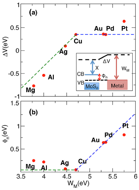
Two regimes can be distinguished in Fig. 1(a). Metals with eV yield a similar , whereas strongly depends on for eV. The cross-over between the two regimes occurs for Cu, where and the SBH is minimal, see Fig. 1(b). The results for the high work function regime are consistent with the common observation that physisorption results in a net decrease of the work function, i.e., a positive . This has been explained in terms of the Pauli exchange repulsion between the electrons of the metal and those of the overlayer yielding a net pushback of electrons into the metal.Bokdam et al. (2014a) The effect is fairly moderate for MoS2, resulting in eV for the high work function metals, and a size that does not depend critically on the details of the metal or the interface structure.
With a constant the SBH simply follows the work function, i.e., the slope , which is the Schottky-Mott rule. This rule is typically found in the absence of any interface states with energies in the semiconductor band gap, which is consistent with the MoS2metal interaction being weak. If ideal Schottky-Mott behavior would persist for the low work function metals, the SBH would vanish for . Clearly this is not the case in Fig. 1(b). The SBH has a minimum at Cu, but it increases again for the low work function metals.
We analyze this behavior for Mg, being the metal with the lowest work function in this study. The band structure of the MoS2Mg(0001) interface is shown in Fig. 2(a). At the optimized equilibrium distance Å, the MoS2 bands are significantly perturbed by the interaction with the substrate. This perturbation can be visualized by comparing the density of states (DoS) of MoS2Mg to that of free-standing MoS2, see Fig. 2(e). The MoS2Mg interaction leads to interface states in the MoS2 band gap that are energetically close to the bottom of the MoS2 conduction band. This is seen most clearly in the difference DoS, i.e. , represented by the green curve in Fig. 2(e), where are the DoSs of the interface, the free-standing adsorbate, and the clean metal substrate, respectively.
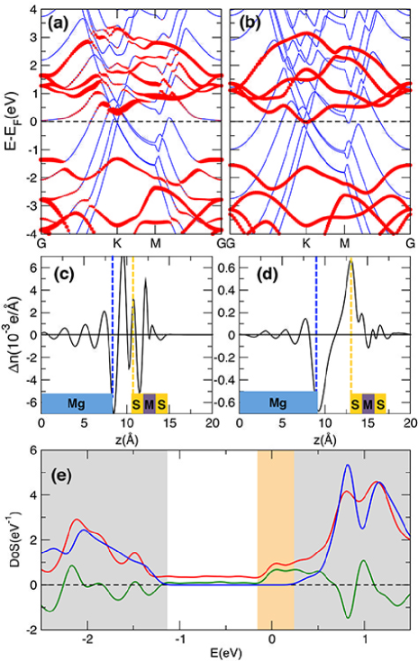
The is negligible for energies inside the MoS2 band gap, except for a region eV below the conduction band edge (shaded orange in Fig. 2(e)). The negative sign of the calculated potential step at the MoS2Mg interface, eV, shows that electronic charge is transferred from the Mg substrate to the MoS2 overlayer. These electrons populate the interface states, thereby pinning the Fermi level in the band gap. For high work function metals the Fermi level is well within the MoS2 gap, where the density of interface states is negligible. The corresponding SBHs then obey the Schottky-Mott rule. It is only for low work function metals, when the Fermi level approaches the bottom of the MoS2 conduction band, that interface states become noticeable and pin the Fermi level.
One can destroy the interface states by breaking the MoS2Mg interaction. This is demonstrated by Fig. 2(b), which gives the band structure of MoS2Mg(0001) with the adsorbant placed at an artificially large distance Å from the metal surface. The MoS2 bands are unperturbed, as there is no chemical interaction with the substrate at this distance. The Fermi level is in the MoS2 conduction band, which is not surprising as the work function of Mg(0001), eV is much smaller than the MoS2 electron affinity eV. The calculated interface potential step, eV, indeed corresponds to , as it should for electron transfer from Mg to MoS2 to equilibrate the Fermi level. It results in a zero SBH, according to Eq. (1).
This interpretation is confirmed by the electron density difference , where are the plane-averaged electron densities of the interface, the free-standing adsorbate, and the clean metal substrate, respectively. At an MoS2Mg distance Å, shows an accumulation of electrons at the position of MoS2, and an electron depletion at the Mg surface, see Fig. 2(d), consistent with an electron transfer from Mg to MoS2, which creates an interface dipole and potential step to equilibrate the Fermi level. At the equilibrium MoS2Mg distance, shows a much more complicated pattern, see Fig. 2(c), which is consistent with an interface interaction that alters the electronic structure.
MoS2h-BNmetal interfaces. A Schottky barrier at a MoS2metal contact is unavoidable, as the interface interaction leads to states that pin the Fermi level below the conduction band. Breaking this interaction by introducing a vacuum spacing at the interface, is not a practical way to make a metal-semiconductor contact. However, inserting an inert layer between the metal and MoS2 can be. This layer has to be sufficiently thin as not to form a high barrier for electron transport. A monolayer of h-BN is ideally suited. A single layer of h-BN can be deposited or grown on a range of metal substrates, and it is stable under ambient conditions. Substrates consisting of a transition metal (111) surface covered by a h-BN monolayer, are widely available. Sandwiching a monolayer of h-BN between two metal electrodes gives metallic conduction,Yazyev and Pasquarello (2009) which indicates that the layer is transparent to electrons.
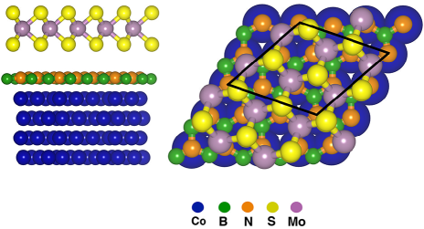
We build MoS2h-BNmetal structures by putting a MoS2 cell on top of a h-BNCo or Ni cell, see Fig. 3, with the h-BN layer in a registry with the underlying metal surface, as in Refs. Bokdam et al., 2014b, a. As before, we fix the lattice constant of MoS2, and adapt the lattices of h-BN and the metal(111) substrates accordingly, which requires a 4% squeeze of the h-BN lattice. A h-BN monolayer is chemisorbed on Co and Ni(111) surfaces, but MoS2 and h-BN are bonded by a weak, van der Waals, interaction. Such interactions are not represented in the PBE functional, so we use the optB88-vdW-DF van der Waals density functional here.
Adsorption of h-BN has a dramatic effect on the work function; it reduces the work functions of Co and Ni(111) by 1.9 eV and 1.8 eV, respectively. These reductions result from large interface dipoles that are formed at the h-BNmetal interfaces, where Pauli exchange repulsion between the electrons at the interface gives an important contribution.Bokdam et al. (2014a) Adsorbants in the form of self-assembled monolayers (SAMs) are commonly proposed in order to modify substrate work functions. However, SAMs often suffer from disorder, which diminishes their effect. Adsorption of h-BN leads to a well-defined structure that is much less susceptible to disorder, and gives a sizable work function lowering. Moreover h-BN presents a surface that not only is chemically relatively inert, but also does not change its structure upon adsorbing further layers.
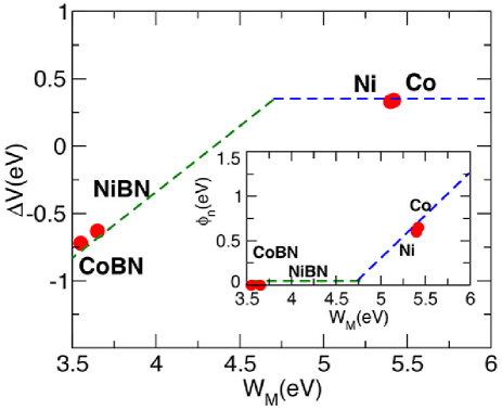
The implications of work function lowering by h-BN adsorption are clearly demonstrated in Fig. 4. Direct adsorption of MoS2 on Co and Ni(111) gives a behavior that is typical for high work function metals. The potential step at the MoS2metal interface is eV, and the SBHs follow the Schottky-Mott rule. In contrast, adsorption of MoS2 on h-BNCo and Ni(111) substrates gives a negative , and it gives a zero SBH. Inserting a h-BN layer has not only effectively decreased the substrate work function, but it has also weakened the MoS2substrate interaction that yielded Fermi level pinning and nonzero SBHs for clean low work function metal substrates.
The difference between adsorbing MoS2 directly onto a clean Co surface and onto a h-BN covered Co surface is observed in the corresponding electronic structures shown in Fig. 5. Direct adsorption onto Co(111) perturbs the MoS2 bands considerably, due to the interaction at the interface, as shown in Fig. 5(a). In contrast, adsorbing MoS2 onto a h-BNCo(111) substrate hardly perturbs the MoS2 bands at all, as demonstrated by Fig. 5(b), which is a clear indication that the interaction between h-BN and MoS2 is weak.
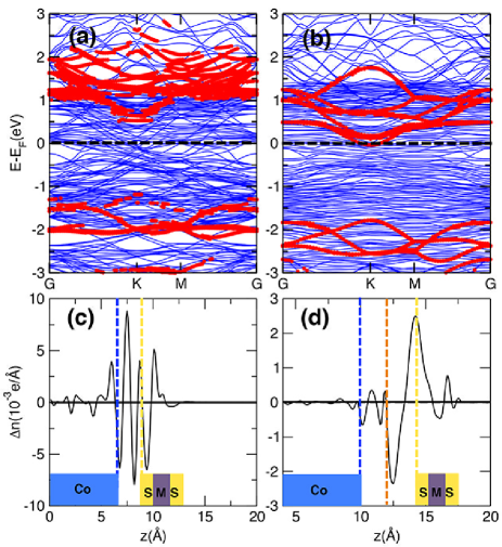
Adsorbing MoS2 directly onto Co leads to the Fermi level being well within the MoS2 band gap, which is not surprising as Co is a high work function metal. In contrast, adsorbing MoS2 onto a h-BNCo substrate yields a Fermi level that is pinned at the bottom of the MoS2 conduction band. The electron density differences shown in Fig. 5(c) and 5(d) substantiate this picture. Figure 5(c) shows the complicated pattern that is typically associated with a direct MoS2metal interaction, compare to Fig. 2(c). for MoS2 on a h-BNCo shows an accumulation of electrons at the position of MoS2, and an electron depletion at the position of the h-BN, which reflects an electron transfer from the substrate to MoS2 to equilibrate the Fermi level, compare Figs 5(d) and 2(d).
Conclusions. We have shown that contacting MoS2 with low work function metals leads to Fermi level pinning at 0.1-0.3 eV below the conduction band edge. This behavior results from the interaction at the interface between the metal and the MoS2, creating a considerable density of interface states just below the MoS2 conduction band. Inserting a boron nitride (BN) monolayer between the metal and the MoS2 destroys these interface states, and recovers the unperturbed MoS2 band structure. In addition, absorbing h-BN on Co(111) or Ni(111) decreases the metal work function by close to 2 eV. We predict that contacting MoS2 with h-BNCo or Ni(111) does not give a Schottky barrier.
Acknowledgement. We thank Menno Bokdam for useful discussions. This work is part of the research program of the Foundation for Fundamental Research on Matter (FOM), which is part of the Netherlands Organisation for Scientific Research (NWO). The use of supercomputer facilities was sponsored by the Physical Sciences Division (EW) of NWO.
References
- Geim and Grigorieva (2013) A. K. Geim and I. V. Grigorieva, Nature 499, 419 (2013).
- Mak et al. (2010) K. F. Mak, C. Lee, J. Hone, J. Shan, and T. F. Heinz, Phys. Rev. Lett. 105, 136805 (2010).
- Radisavljevic et al. (2011) B. Radisavljevic, A. Radenovic, J. Brivio, V. Giacometti, and A. Kis, Nat. Nanotechnol. 6, 147 (2011).
- Wang et al. (2012a) Q. H. Wang, K. Kalantar-Zadeh, A. Kis, J. N. Coleman, and M. S. Strano, Nat. Nanotechnol. 7, 699 (2012a).
- Wang et al. (2012b) H. Wang, L. Yu, Y.-H. Lee, Y. Shi, A. Hsu, M. L. Chin, L.-J. Li, M. Dubey, J. Kong, and T. Palacios, Nano Lett. 12, 4674 (2012b).
- Lince et al. (1987) J. R. Lince, D. J. Carré, and P. D. Fleischauer, Phys. Rev. B 36, 1647 (1987).
- Liu et al. (2012) H. Liu, A. T. Neal, and P. D. Ye, ACS Nano 10, 8563 (2012).
- Das et al. (2013) S. Das, H.-Y. Chen, A. V. Penumatcha, and J. Appenzeller, Nano Lett. 13, 100 (2013).
- Chen et al. (2013a) J.-R. Chen, P. M. Odenthal, A. G. Swartz, G. C. Floyd, K. Y. L. Hua Wen, and R. K. Kawakami, Nano Lett. 13, 3106 (2013a).
- Fontana et al. (2013) M. Fontana, T. Deppe, A. K. Boyd, M. Rinzan, A. Y. Liu, M. Paranjape, and P. Barbara, Sci. Rep. 3, 1634 (2013).
- Kaushik et al. (2014) N. Kaushik, A. Nipane, F. Basheer, S. Dubey, S. Grover, M. M. Deshmukh, and S. Lodha, Appl. Phys. Lett. 105, 113505 (2014).
- Kang et al. (2014a) J. Kang, W. Liu, and K. Banerjee, Appl. Phys. Lett. 104, 093106 (2014a).
- Tung (2014) R. T. Tung, Appl. Phys. Rep. 1, 011304 (2014).
- Gong et al. (2014) C. Gong, L. Colombo, R. M. Wallace, and K. Cho, Nano Lett. 14, 1714 (2014).
- Popov et al. (2012) I. Popov, G. Seifert, and D. Tománek, Phys. Rev. Lett. 108, 156802 (2012).
- Chen et al. (2013b) W. Chen, E. J. G. Santos, W. Zhu, E. Kaxiras, and Z. Zhang, Nano Lett. 13, 509 (2013b).
- Kang et al. (2014b) J. Kang, W. Liu, D. Sarkar, D. Jena, and K. Banerjee, Phys. Rev. X 4, 031005 (2014b).
- Bokdam et al. (2011) M. Bokdam, P. A. Khomyakov, G. Brocks, Z. Zhong, and P. J. Kelly, Nano Lett. 11, 4631 (2011).
- Gillen et al. (2014) R. Gillen, J. Robertson, and J. Maultzsch, Phys. Rev. B 90, 075437 (2014).
- Kresse and Hafner (1993) G. Kresse and J. Hafner, Phys. Rev. B 47, 558 (1993).
- Blöchl (1994) P. E. Blöchl, Phys. Rev. B 50, 17953 (1994).
- Kresse and Furthmüller (1996) G. Kresse and J. Furthmüller, Phys. Rev. B 54, 11169 (1996).
- Kresse and Joubert (1999) G. Kresse and D. Joubert, Phys. Rev. B 59, 1758 (1999).
- Bokdam et al. (2014a) M. Bokdam, G. Brocks, and P. J. Kelly, Phys. Rev. B 90, 201411(R) (2014a).
- Perdew et al. (1996) J. P. Perdew, K. Burke, and M. Ernzerhof, Phys. Rev. Lett. 77, 3865 (1996).
- Dion et al. (2004) M. Dion, H. Rydberg, E. Schröder, D. C. Langreth, and B. I. Lundqvist, Phys. Rev. Lett. 92, 246401 (2004).
- Klimeš et al. (2011) J. Klimeš, D. R. Bowler, and A. Michaelides, Phys. Rev. B 83, 195131 (2011).
- Perdew and Zunger (1981) J. P. Perdew and A. Zunger, Phys. Rev. B 23, 5048 (1981).
- Bokdam et al. (2014b) M. Bokdam, G. Brocks, M. I. Katsnelson, and P. J. Kelly, Phys. Rev. B 90, 085415 (2014b).
- Yazyev and Pasquarello (2009) O. Yazyev and A. Pasquarello, Phys. Rev. B 80, 035408 (2009).