Enhanced superconductivity at the interface of W/Sr2RuO4 point contact
Abstract
Differential resistance measurements are conducted for point contacts (PCs) between tungsten tip approaching along the axis direction and the plane of Sr2RuO4 single crystal. Three key features are found. Firstly, within 0.2 mV there is a dome like conductance enhancement due to Andreev reflection at the normal-superconducting interface. By pushing the W tip further, the conductance enhancement increases from 3% to more than 20%, much larger than that was previously reported, probably due to the pressure exerted by the tip. Secondly, there are also superconducting like features at bias higher than 0.2 mV which persists up to 6.2 K, resembling the enhanced superconductivity under uniaxial pressure for bulk Sr2RuO4 crystals but more pronounced here. Third, the logarithmic background can be fitted with the Altshuler-Aronov theory of tunneling into quasi two dimensional electron system, consistent with the highly anisotropic electronic system in Sr2RuO4.
The layered perovskite ruthenate Sr2RuO4 (SRO) has shown evidence for spin-triplet, odd-parity superconductivity (SC) which may be useful for topological quantum computation. Maeno et al. (1994); Mackenzie and Maeno (2003); Maeno et al. (2012) The possible chiral orbital order parameter for the two-dimensional SC is as suggested by the time-reversal symmetry breaking experiments. Luke et al. (1998); Xia et al. (2006) Such chiral order is expected to generate edge currents, but the expected magnetic field due to edge currents has not been directly observed with local field imaging, Kirtley et al. (2007); Hicks et al. (2010); Curran et al. (2014) though there is indirect evidence of edge currents revealed by in-plane tunneling spectroscopy Kashiwaya et al. (2011, 2014) and point contact spectroscopy (PCS), Laube et al. (2000)both with assumptions to fit the conductance spectra.
The surface properties of SRO is very critical for field imaging with scanning quantum interference devices, as well as for the tunneling and point contact spectroscopy. It is known that the SRO surface can undergo reconstruction and the intrinsic SC may not be probed, Upward et al. (2002); Firmo et al. (2013) and it may even show ferromagnetism (FM) due to lattice distortion. Matzdorf et al. (2000) Very careful in situ preparation of devices is required for making good tunnel junctions using microfabrication techniques. Kashiwaya et al. (2011) Recently there is also theory proposal that surface disorder indeed can destroy the spontaneous currents. Lederer et al. (2014)
One way to overcome the surface problem is to use a hard tip for the point contact (PC) measurement. If the tip is hard enough, it may pierce through the surface dead layer and probe the SC underneath. Gonnelli et al. (2002) In fact, for this reason tungsten tip has been used for PCS of heavy fermion superconductors. Gloos et al. (1996) A consequence of using a hard tip is that the tip will exert some pressure on the surface which may affect the SC, Daghero and Gonnelli (2010) possibly due to local distortion of lattice. Gloos et al. (1995); Miyoshi et al. (2005) It is known that for SRO a very low uniaxial pressure of 0.2 GPa along the axis can enhance the superconducting transition temperature () of pure SRO from 1.5 K up to 3.2 K, Kittaka et al. (2010, 2009) and recently in-plane strain (0.23%) along direction is also shown to enhance from 1.3 K up to 1.9 K. Hicks et al. (2014) The pressure in abovementioned measurements were applied to bulk samples, while for PCS the pressure is exerted locally. In the latter case it may be less affected by the inhomogenity of the applied pressure and the sample is less tend to developing cracks, thus locally higher pressure may be reached though absolute pressure is not known. Here we report greatly enhanced SC observed at the interface of the point contact junction between a tungsten tip approaching along the axis direction and the plane surface of a SRO single crystal.
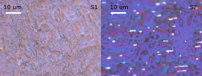
SRO single crystals are grown by floating zone methods and are from two different batches, details of sample preparation can be found in previous reports. Mao et al. (2000) Sample S1 is from the first batch and is easier to cleave and shows no Ru inclusions. Sample S2 is from the second batch, too hard to cleave, and contains a lot of Ru inclusions (for optical images see Appendix C). Only on the cleaved surface of S1 do we observe SC feature. Tungsten wire of 0.25 mm diameter is etched to form the tip, and then fixed pointing to the plane of the SRO sample. A Si chip with the sample and thermometer glued on top is mounted on an attoCube nanopositioner stack. Since the tip and sample are both fixed to the copper housing, relative displacement between the tip and sample is suppressed, which ensures a stable contact and reproducible PCS. The housing is suspended with springs at the bottom of a insertable probe for a Leiden dilution fridge. With such customization the sample position is not at the field center of the magnet, and the field value is estimated with the tabled values from the magnet manufacturer. Differential resistance () is measured with standard lock-in technique.
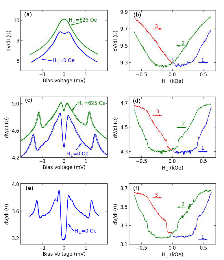
At the same location, by pushing the tungsten tip towards the SRO surface (more precisely it is the SRO moving towards the tip), the PC resistance is reduced and the pressure is increased. The zero bias and zero field resistance () is: 9.3, 4.3, 3.2 respectively (see Appendix A for a discussion of PC resistance). The bias dependence of is shown in Figs. 1a, 1c, and 1e, at nominal temperature 0.35 K. SC is clearly shown by the resistance dip within 0.2 mV without any applied field. With a 625 Oe magnetic field applied along the axis (H⟂), SC is almost fully suppressed for the 9.3 PC as shown by the recover of the resistance peak at zero bias. However, for the 4.3 PC there is still a small dip, suggesting that SC is not fully suppressed, i.e., SC is enhanced with increased pressure.
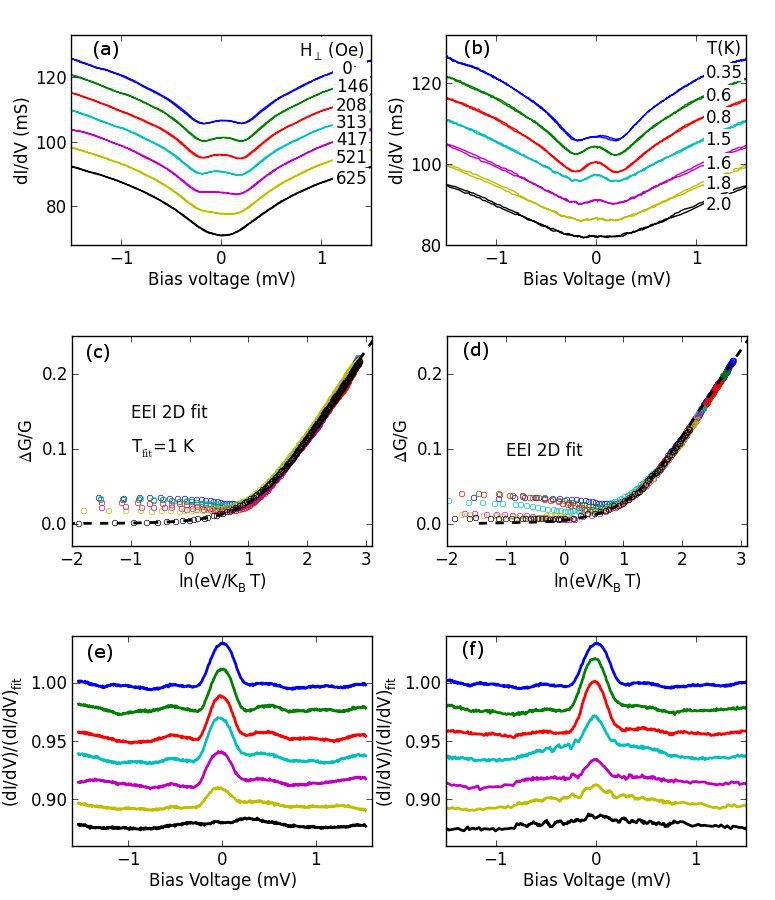
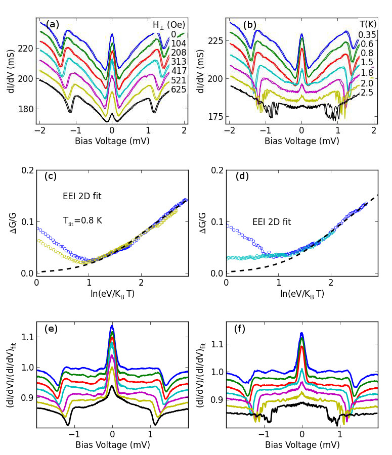
Enhancement of SC is further confirmed by the temperature dependence of at zero field as shown in Fig. 2b and Fig. 3b, where is increased from the bulk value of 1.5 k to about 2 K and 2.5 K for the 9.3 and 4.3 PC respectively. This enhanced Tc is consistent with previous susceptibility measurements on bulk SRO sample under uniaxial pressure, where the mechanism of enhancement was ascribed to anisotropic lattice distortion, Kittaka et al. (2009, 2010); Taniguchi et al. (2012) similar to that found in the eutectic 3K phase. Ying et al. (2009, 2013) In Figs. 2 and 3, for easy comparison with theoretical description, is converted to .
The magnetoresistance (MR) is shown in Figs. 1b, 1d, and 1f for the three PCs. The resistance starts to increase quickly at around 400 Oe, and there is clearly a hysteresis with steps which gets sharper and more pronounced for higher PC pressure. MR hysteresis is usually observed for ferromagnetic samples, and the observation of both SC and MR hysteresis was linked to the coexistence of SC and ferromagnetism (FM) for SC at the oxides interface. Dikin et al. (2011) If indeed a FM-like internal field exists, could it be related to the long sought-after time-reversal symmetry-breaking fields? Kirtley et al. (2007); Hicks et al. (2010); Curran et al. (2014)
First the possibility of conventional vortex pinning needs be considered. The field value above which starts to increase quickly is around 400 Oe, in the same order of magnitude with the upper critical field about 710 Oe for pure SRO crystal, but much larger than the critical field about 70 Oe (by specific heat measurements). Deguchi et al. (2004) Sharp increase of resistance may indicate that vortices enter the PC interface and SC is suppressed. However, it is not clear whether such strong pinning could be reduced by PC. The average distance between vortices is , about 0.3 m for 400 Oe, so the diameter of the PC should be much larger to include multiple vortices, which is inconsistent with conventional understanding of the PC. Moreover, it is difficult to explain why the step-like features become sharper with higher pressure. Besides the external pinning due to defects, the intrinsic pinning due to chiral domain wall Dumont and Mota (2002) seems also unlikely to reach 400 Oe. One variation of vortex pinning is chiral domain wall motion, where with ramping field the DW wall moves and the edge current can affect the transport of the PC, Kambara et al. (2008) which seems reasonable.
Surface FM also needs to be considered since among other layered perovskite ruthenates in the series , SrRuO3 is a ferromagnetic metal with Tc=160 K, and Sr3Ru2O7 is at the boarder of FM and shows pressure-induced FM. Ikeda et al. (2000) Thus it is natural to expect that FM could be induced for SRO, or there might be some eutectic phase Mao et al. (2000) on the surface which leads to FM. Previously, experimental attempts to measure the bulk magnetic susceptibility of SRO with uniaxial pressure were not successful, since above 0.4 Gpa SRO sample tends to crush, Ikeda et al. (2004) while no drastic change of the temperature dependence of susceptibility was observed. On the other hand, doping the Sr with Ca does show a ground state of static magnetic order due to rotation of octahedra. Carlo et al. (2012); Ortmann et al. (2013) Thus it is possible that the pressure under the tip may be higher than 0.4 GPa Gonnelli et al. (2002) and its influence is comparable with that by doping. However, this is inconsistent with the fact that the hysteresis diminishes together with SC at higher temperatures, which also indicates that the hysteresis is not due to eutectic phase impurities.
Both field and temperature dependences of resemble those found for in-plane Au/SRO tunneling junctions in Ref. [Kashiwaya et al., 2011], as shown by detailed field and temperature dependences in Fig. 2 and Fig. 3, for the 9.3 and 4.3 PC respectively. However, in Ref. [Kashiwaya et al., 2011] the gap is about 0.7 mV instead of 0.2 mV, and the conductance enhancement of the dome like feature is less than 1% (see see Appendix D for similar PC spectra with a Au tip). The dome like feature may be fitted considering chiral p-wave symmetry Kashiwaya et al. (2011), but here we focus on experimental findings and methodology while leave the fittings in the future.
The broad background resistance hump as shown by at 625 Oe in Fig. 4(a) (same as in Fig. 1a) is generally called zero-bias anomaly (ZBA), which is frequently observed in tunnel junctions Kashiwaya et al. (2011) as well as PCs. Gloos (2009); Gloos and Tuuli (2012) The possible origins for ZBA in PCs include “extrinsic” magnetic impurities, two-level systems, Kondo scattering due to spontaneous electron spin polarization etc, as well as “intrinsic” density of states (DOS) effect, as shown for chromium where DOS is reduced due to the spin density wave gap, Meekes (1988) and more recently for iron pnictides where DOS is enhanced due to strong electron correlations. Arham et al. (2012) Here ZBA apparently coexists with SC in SRO, which is very sensitive to impurities, thus the origin of ZBA is more likely due to some “intrinsic” origin.
The background ZBA can be normalized when the bias dependence is replotted using . In Figs. 2(c) and 2(d), the normalized change of conductance shows a linear dependence for , similar to what was observed in tunneling measurements for disordered metal films, Gershenzon et al. (1986) and also for layered cuprates and manganites. Abrikosov (2000); Mazur et al. (2007) In the tunneling case, the reduction of DOS is due to electron-electron interaction (EEI). As proposed by Altshuler and Aronov, Al’tshuler and Aronov (1979); *Altshuler1980; *Altshuler1985 for low dimensional systems the exchange interaction between electrons can cause quantum corrections to the conductivity as well as DOS, which depends on the dimensionality of the systems. For , the DOS correction in 2D (see Appendix B for details). When the full formula is used, we get good fits in the full bias range as shown by the dashed lines in Figs. 2(c) and 2(d) (also in Figs. 1a and b). We note that in order for all normalized curves to collapse onto a single curve, enhanced temperature () needs to be assumed for measured at lower temperatures. This may indicate there is local heating in the small PC region, possibly due to inadequate filtering of the external microwave noise. Liu et al. (2014)
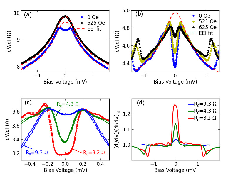
The fitted ZBA can be considered as the normal state background and divided from the normalized conductance, Kashiwaya et al. (2011) the resulted curves are shown in Figs. 2(e) and 2(f), with the dome like conductance enhancement well demonstrated. Another feature of the PC spectra is a small periodic “wiggling” outside 0.2 mV, which also diminishes with increasing field and temperature, suggesting that it is probably due to interference of quasiparticles at the NS interface. Similar feature was also observed for multiple band superconductor MgB2 Gonnelli et al. (2002); Daghero and Gonnelli (2010) but detailed analyses are lacking. The ZBA background becomes less pronounced when the PC resistance is reduced from 9.3 to 4.3 , as shown in Figs. 3c and d, while the conductance enhancement gets larger. This is better illustrated by the normalized enhancement (Fig. 4d), and by direct comparison of the zero field (Fig. 4c).
What parameters may change when the PC resistance is reduced from 9.3 to 4.3 ? In the standard theory for PCS (see Appendix A for details), the PC resistance
| (1) |
where is the Sharvin resistance corresponding to the ballistic limit, and is the Maxwell resistance corresponding to the diffusive limit and related to the resistivity. For the simplest metallic PC, is considered to be energy independent as the energy dependence of velocity cancels that of the DOS. This can be changed when complicated Fremi surface is involved and the effective DOS may be probed by . Meekes (1988); Arham et al. (2012) Here for single crystal SRO the mean free path is large, and if the interface is clean and barrier-free, the PC should be close to the ballistic limit. As and , where is the diameter of PC, and if the anisotropic electronic state in SRO is not considered, the reduction of resistance from 9.3 to 4.3 would lead to an increase of by roughly =1.47 times in the ballistic limit (twice increase of the area); or by 2 times in the thermal limit(quadruple increase of the area).
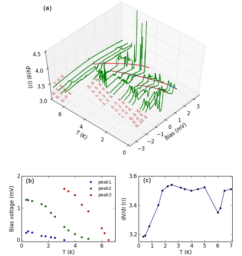
With the increase of contact area, the PC may show a larger critical current () if the critical current density is constant and is only determined by the PC itself. As the additional dips shown in Fig. 3 is ascribed to the critical current effect Sheet et al. (2004), can be estimate from the dip position. At 1.6 K the dip position is about 1.2 and 2.3 mV for the 4.3 and 9.3 PCs, so the calculated is around 0.28 and 0.25 mA respectively, inconsistent with the expected 2-4 times increase of if is proportional to the contact area. This may suggest that is determined by a fixed region, e.g., chiral domains under the PC, instead of by the area of the PC itself. Thus, with increasing bias the region of SRO under the PC reaches its , and shows a finite increase due to , as described in Eq.(1).
When the PC resistance is reduced further to 3.2 , even larger conductance enhancement is observed as shown in Fig. 1e and Fig. 4. After normalization by the background, the conductance enhancement at zero bias is about 3% for the 9.3 PC, 14% for the 4.3 PC, and 22% for the 3.2 PC (Fig. 4d). The original curves without normalization and the EEI fits are also shown in Figs. 4a and b, and the fits can very well reproduce the curves when an effective temperature is taken into account. Zoom-in the zero bias regime, the absolute amplitude of the dip and of the “wiggling” part outside of the dip are clearly shown in Fig. 4c. For all three PCs, the dip evolves to ZBA at around 0.2 mV (Fig. 4c), which is consistent with the gap value of SRO from the weak-coupling theory () with K. This value is much smaller compared with previous PCS and plane tunneling results where 0.7-0.9 mV were obtained, Laube et al. (2000); Kashiwaya et al. (2011) and also smaller compared with scanning tunnel spectroscopy (STS) measurements where 0.3-0.5 mV were reported. Upward et al. (2002); Firmo et al. (2013)
For the 3.2 PC, the surprising feature that the critical current effect persists to much higher temperatures is better illustrated in Fig. 5. In Fig. 5a, besides the first peak at around 0.2 mV, there are two additional peaks, one persists up to about 5 K, while the other persists up to about 6.2 K. These two peaks are likely to be SC features as the measured MR up to around 625 Oe also shows hysteresis, which decreases with increasing temperature and diminishes along with the resistance dip near zero bias. At 8 K, the within 1.5 mV, and the MR of the zero bias within 625 Oe, becomes practically flat and changes less than 0.03 . The temperature dependence of the position of peaks is plotted in Fig. 5b, and the zero bias from the spectra in Fig. 5a is plotted in Fig. 5c. There are clearly two resistance drops at around 4 and 6 K, and we note a similar but smaller drop around 4 k was also observed in Ref. [Kashiwaya et al., 2011]. Since the bulk 1.5 K for S1, and even for the 3-K phase 3 K, thus the greatly enhanced could be only due to the W/SRO PC.
In summary, an ultralow temperature point contact setup using nanopositioners was used to measure differential resistance of W/SRO point contact junctions. We find: 1) a superconducting gap around 0.2 mV and a dome like shape of conductance enhancement, consistent with chiral p-wave symmetry; 2) SC-like features persisting up to 6.2 K, much higher than the bulk Tc of SRO, presumably due to the pressure exerted by the W tip and a mechanism similar to that of the 3K-phase; 3) a broad resistance hump coexisting with superconductivity, which is ascribed to density of states effect due to 2D electron-electron interaction, consistent with the highly anisotropic electronic system of SRO. We believe PCS may provide useful information beyond the surface problem for SRO.
We thank Hu JIN for contribution in the earlier stage of this project, Liang LIU for various help with experiments and data analysis, Xin LU for helpful discussions on point contact measurements, and Fa WANG for discussions on correlated systems respectively. Work at Peking University is supported by National Basic Research Program of China (973 Program) through Grant No. 2011CBA00106 and No. 2012CB927400. The work at Tulane is supported by the DOE under grant DE-SC0012432.
Appendix A Basics of point contact resistance
There are many reviews on point contact spectroscopy Duif et al. (1989) and particular on unconventional heavy fermion systems. Naidyuk and Yanson (1998); Park and Greene (2009) Here we introduce the basics of the PC resistance following Ref. Naidyuk and Yanson, 1998.
In the simple theoretical model, PC is formed with an orifice with diameter between two bulk metallic electrodes. Depending on the relative ratio between and different mean free path , PC can be categorized into three regimes: ballistic (), diffusive (), and thermal (). In the ballistic regime, the Fermi surface in the two electrodes has a difference of , similar to the tunneling junction case; while in the thermal regime, the Fermi surface evolves smoothly within the PC and there is a well defined equilibrium temperature profile. Pothier et al. (1997)
The current density in the orifice along its normal direction (-axis) is
| (2) |
where is the electron velocity, and is the Fermi-Dirac distribution function. For a voltage biased ballistic PC, considering the energy difference ,
| (3) |
where is the electronic DOS. In the simplified case, is inversely proportional to , thus there is no non-linearity caused by energy dependence of DOS. The resulted Ohmic resistance is
| (4) |
where is the bulk resistivity, the elastic mean free path, k the quantum resistance. With the assumption that the Drude picture holds, is a constant for a particular metal (Note that the quantities and were used in the original derivation). Thus, in the ballistic regime the diameter of the orifice can be estimated using the zero bias resistance . To get a rough number, in the case of copper and other simple metals, nm.
At finite bias, the electron can also be backscattered by phonons, magnons etc, at characteristic bias energy. So - curve of the ballistic PC can be nonlinear and second derivative is often used to identify phonon and magnon spectra. More generally, for correlated materials with complex Fermi surface, is no longer inversely proportional to , - curve is nonlinear and may reflect the change of DOS. Meekes (1988); Arham et al. (2012)
For PC in the diffusive or thermal regime, electrons in the PC are scattered by impurities or defects, whose contribution to can be estimated from the bulk resistivity, and the orifice just provides a geometric limitation. In the limit , the Maxwell resistance is
| (5) |
As it depends on instead of , it dominates over when is large. And when inelastic scattering happens inside the PC, the equilibrium temperature in the PC can be elevated following
| (6) |
where is the Lorentz number. For a rough estimation, when , assume a standard V2K-2, then , or (K) 3.2 (mV). That explains for a thermal PC similar feature can be found in and in . For the gap energy around 0.2 mV in this work, in the thermal limit a rough estimation of at 0.2 mV is 0.64 K, which is below the of SRO, so the bias will not drive the PC out of the SC state even in the thermal limit.
In the intermediate regime, Wexler derived an interpolation formula
| (7) |
For a heterocontact between two different electrodes (1 and 2), the resistance has contribution from both sides. For geometrically symmetric PC with almost equal ,
| (8) |
Since the resistivity of simple metal tip like tungsten is usually much smaller than that of the correlated electron systems (in normal state), we may just keep the resistivity term of the correlated systems being probed. The assumption of equal is very rough, the difference between of tungsten and SRO is shown in Table 1. Here of tungsten is roughly estimated by assuming two valence electrons and simple spherical Fermi surface.
| Fermi sheet | Tungsten | |||
|---|---|---|---|---|
| () | 0.304 | 0.622 | 0.753 | 1.55 |
| () | ||||
| () | 3.3 | 7.0 | 16 | 1 |
For a heterocontact between a normal metal and a superconductor, Blonder-Tinkham-Klapwijk (BTK) model Blonder et al. (1982) is widely used to explain the conductance enhancement within the gap energy and a tunnel barrier parameter is used to characterize the interface. Whether the Fermi velocity mismatch can be represented with an effective parameter is not yet clear. Park and Greene (2009) Note that in BTK model the scattering in the metals and the interface is not considered, even for finite . So its transparent interface limit () corresponds to the ballistic limit of the PC model, i.e., the point contact Andreev reflection spectroscopy can only be applied to ballistic contacts. Since the BTK model can be used for various interface transparencies, it has wider application than the simple point contact model. To take into account additional scattering at or near the interface, i.e., , a normal resistor in series Sheet et al. (2004) or a normal current in parallel Miyoshi et al. (2005); Peng et al. (2013) can be added. Thus even in the so-called thermal regime, the gap value can be roughly estimated with consideration of a combination of the BTK model and PC model. Sheet et al. (2004)
In some cases it is believed that although the footprint of the PC can be tens of microns, much larger than , but still ballistic limit can be applied because there are multiple smaller PC junctions randomly distributed across the contact area, Bugoslavsky et al. (2005); Peng et al. (2013) and the BTK model can be used directly. Although conceptually this is different from the picture that there is an interface barrier which contributes to the PC resistance like a real tunneling junction, but in both cases ballistic limit can be applied as is smaller than .
When the SC has unconventional pairing symmetries, generalized BTK model is developed to fit the data by taking into account various parameters including order parameter symmetry, incidence angle, Fermi surface mismatch, life time broadening due to inter or intra band scattering etc. PCS for unconventional SC has been reviewed in Ref. Gloos et al., 1996; Park and Greene, 2009; Daghero and Gonnelli, 2010; Daghero et al., 2013. It is still not clear whether the order parameter symmetry can be verified strictly from the shape of the point contact Andreev reflection spectra. Gloos et al. (1996); Park and Greene (2009) In this work we mainly report the temperature and field dependence of the PC spectra rather than quantitatively fit the data with the generalized BTK model. Kashiwaya et al. (2011, 2014)
Appendix B Fitting with electron-electron interaction
The difference between PCS and planar tunneling is whether the in-plane momentum is conserved. Since there is no well-known theory for incorporation of quantum correction of DOS into PCS, here we use the theory for the planar tunneling junctions.
Correction to tunneling conductance by electron-electron interaction (EEI) is quantitatively described by the Altshuler-Aronov (AA) theory, Altshuler and Aronov (1985); Gershenzon et al. (1986) in the 2D limit,
| (9) |
where is the resistance per square of the metal film, the thickness of the insulating barrier, the diffusion constant, and a integral for 2D as defined in Ref. [Gershenzon et al., 1986]. The integral is
| (10) | ||||
where and .
The prefactor before the bracket in Eq. (9) can be lumped into one parameter and it is the only fitting parameter. When but still within the 2D limit, Eq. (9) approaches and is just the slope shown in Fig. 2. Since , the thickness of the metal film, the resistivity , the slope , where is a constant.
For the 3D limit,
| (11) |
which shows a linear dependence on when .
Appendix C Optical images of the SRO surface
Optical images for SRO samples S1 and S2 are shown in Fig. 6 for comparison. Dense Ru inclusions of width about 1 m and length a few m are clearly seen in the micro image for S2, which is also harder to cleave than S1. This is consistent to the observation of Lichtenberg in Ref. Lichtenberg, 2002 that SRO with Ru vacancies is much easier to cleave and the surface dead layer probably is also easier to pierce through. We note that although here the surface was polished by sandpaper to improve image quality, the Ru inclusions can easily be observed on the surface of S2 without any treatment.
Appendix D Reproducibility
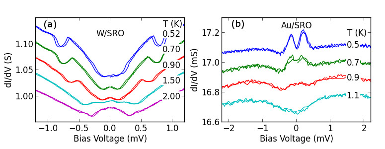
PC spectra for more than 10 locations were measured in several runs. In each run a few locations are tried to search for SC-like features. With increasing force the tip eventually became blunted and bent, and small cracks can also develop on the surface of the SRO. A set of PC spectra similar to that in Fig. 3 is shown in Fig. 7a, for a W/SRO PC on S1 but obtained in another run. Besides W tip, Au tip (0.5 mm dia.) was also tried on S1 and the PC spectra are shown in Fig. 7b. For the Au/SRO PC, gap value around 0.5 mV is observed, the conductance enhancement is only about 1%, and instead of the dome like conductance peak, a split peak is observed, similar to that was reported in Ref. [Kashiwaya et al., 2011].
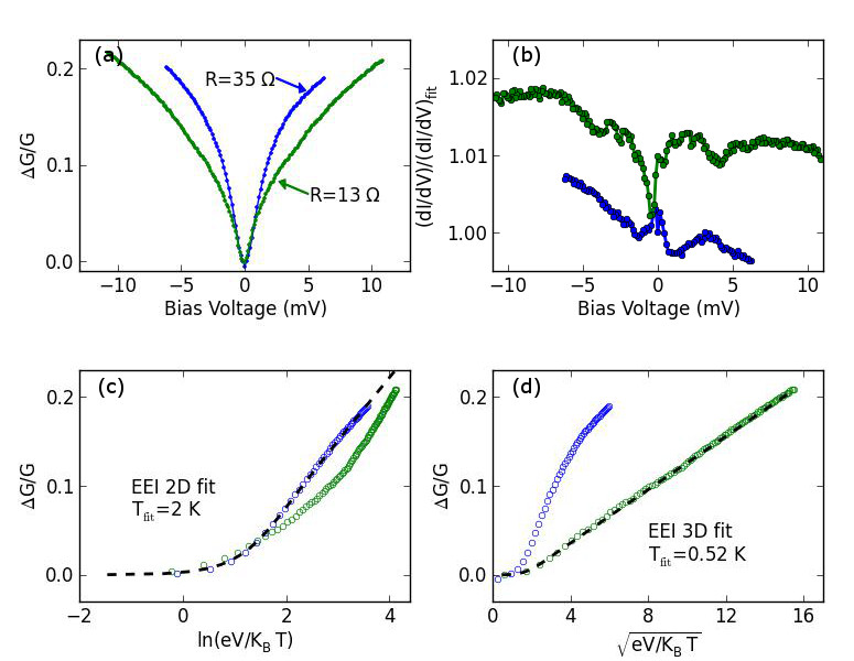
ZBA is less obvious for Au/SRO PCs. For W/SRO PCs, ZBA is frequently observed, which could be due to a thin oxide layer or a defective layer on the surface as observed in other PC measurements. Sasaki et al. (2011); Peng et al. (2013) For those PC spectra showing clear ZBA, there are two typical types as shown in Fig. 8. One type is similar to that in Fig. 2 with a logarithmic dependence consistent with 2D EEI, and SC feature sometimes coexists with ZBA; the other type has a dependence which is consistent with 3D EEI, no SC feature is observed with this type of ZBA. For the 2D EEI type, e.g., for a 35 PC on S2 as shown in Fig. 8, the slope 0.07 is close to the slope 0.11 for S1 in Fig. 2, and 0.08 in Fig. 3, indicating similar 2D EEI is probed, though here = 2 K is higher than the bath temperature about 0.52 K, which is probably the reason that SC feature is not observed.
References
- Maeno et al. (1994) Y. Maeno, H. Hashimoto, K. Yoshida, S. Nishizaki, T. Fujita, J. G. Bednorz, and F. Lichtenberg, Nature 372, 532 (1994).
- Mackenzie and Maeno (2003) A. P. Mackenzie and Y. Maeno, Rev. Mod. Phys. 75, 657 (2003).
- Maeno et al. (2012) Y. Maeno, S. Kittaka, T. Nomura, S. Yonezawa, and K. Ishida, Journal of the Physical Society of Japan 81, 011009 (2012), http://journals.jps.jp/doi/pdf/10.1143/JPSJ.81.011009 .
- Luke et al. (1998) G. M. Luke, Y. Fudamoto, K. M. Kojima, M. I. Larkin, J. Merrin, B. Nachumi, Y. J. Uemura, Y. Maeno, Z. Q. Mao, Y. Mori, H. Nakamura, and M. Sigrist, Nature 394, 558 (1998), cond-mat/9808159 .
- Xia et al. (2006) J. Xia, Y. Maeno, P. T. Beyersdorf, M. M. Fejer, and A. Kapitulnik, Phys. Rev. Lett. 97, 167002 (2006).
- Kirtley et al. (2007) J. R. Kirtley, C. Kallin, C. W. Hicks, E.-A. Kim, Y. Liu, K. A. Moler, Y. Maeno, and K. D. Nelson, Phys. Rev. B 76, 014526 (2007).
- Hicks et al. (2010) C. W. Hicks, J. R. Kirtley, T. M. Lippman, N. C. Koshnick, M. E. Huber, Y. Maeno, W. M. Yuhasz, M. B. Maple, and K. A. Moler, Phys. Rev. B 81, 214501 (2010).
- Curran et al. (2014) P. J. Curran, S. J. Bending, W. M. Desoky, A. S. Gibbs, S. L. Lee, and A. P. Mackenzie, Phys. Rev. B 89, 144504 (2014).
- Kashiwaya et al. (2011) S. Kashiwaya, H. Kashiwaya, H. Kambara, T. Furuta, H. Yaguchi, Y. Tanaka, and Y. Maeno, Phys. Rev. Lett. 107, 077003 (2011).
- Kashiwaya et al. (2014) S. Kashiwaya, H. Kashiwaya, K. Saitoh, Y. Mawatari, and Y. Tanaka, Physica E: Low-dimensional Systems and Nanostructures 55, 25 (2014), topological Objects.
- Laube et al. (2000) F. Laube, G. Goll, H. v. Löhneysen, M. Fogelström, and F. Lichtenberg, Phys. Rev. Lett. 84, 1595 (2000).
- Upward et al. (2002) M. D. Upward, L. P. Kouwenhoven, A. F. Morpurgo, N. Kikugawa, Z. Q. Mao, and Y. Maeno, Phys. Rev. B 65, 220512 (2002).
- Firmo et al. (2013) I. A. Firmo, S. Lederer, C. Lupien, A. P. Mackenzie, J. C. Davis, and S. A. Kivelson, Phys. Rev. B 88, 134521 (2013).
- Matzdorf et al. (2000) R. Matzdorf, Z. Fang, Ismail, J. Zhang, T. Kimura, Y. Tokura, K. Terakura, and E. W. Plummer, Science 289, 746 (2000), http://www.sciencemag.org/content/289/5480/746.full.pdf .
- Lederer et al. (2014) S. Lederer, W. Huang, E. Taylor, S. Raghu, and C. Kallin, Phys. Rev. B 90, 134521 (2014).
- Gonnelli et al. (2002) R. S. Gonnelli, A. Calzolari, D. Daghero, G. A. Ummarino, V. A. Stepanov, P. Fino, G. Giunchi, S. Ceresara, and G. Ripamonti, Journal of Physics and Chemistry of Solids 63, 2319 (2002), cond-mat/0107239 .
- Gloos et al. (1996) K. Gloos, F. Anders, B. Buschinger, C. Geibel, K. Heuser, F. Jährling, J. Kim, R. Klemens, R. Müller-Reisener, C. Schank, and G. Stewart, Journal of Low Temperature Physics 105, 37 (1996).
- Daghero and Gonnelli (2010) D. Daghero and R. S. Gonnelli, Superconductor Science and Technology 23, 043001 (2010).
- Gloos et al. (1995) K. Gloos, F. Martin, C. Schank, C. Geibel, and F. Steglich, Physica B: Condensed Matter 206-207, 279 (1995), proceedings of the International Conference on Strongly Correlated Electron Systems.
- Miyoshi et al. (2005) Y. Miyoshi, Y. Bugoslavsky, and L. F. Cohen, Phys. Rev. B 72, 012502 (2005).
- Kittaka et al. (2010) S. Kittaka, H. Taniguchi, S. Yonezawa, H. Yaguchi, and Y. Maeno, Phys. Rev. B 81, 180510 (2010).
- Kittaka et al. (2009) S. Kittaka, H. Yaguchi, and Y. Maeno, Journal of the Physical Society of Japan 78, 103705 (2009), http://journals.jps.jp/doi/pdf/10.1143/JPSJ.78.103705 .
- Hicks et al. (2014) C. W. Hicks, D. O. Brodsky, E. A. Yelland, A. S. Gibbs, J. A. N. Bruin, M. E. Barber, S. D. Edkins, K. Nishimura, S. Yonezawa, Y. Maeno, and A. P. Mackenzie, Science 344, 283 (2014), http://www.sciencemag.org/content/344/6181/283.full.pdf .
- Mao et al. (2000) Z. Mao, Y. Maenoab, and H. Fukazawa, Materials Research Bulletin 35, 1813 (2000).
- Taniguchi et al. (2012) H. Taniguchi, S. Kittaka, S. Yonezawa, H. Yaguchi, and Y. Maeno, Journal of Physics: Conference Series 391, 012108 (2012).
- Ying et al. (2009) Y. A. Ying, Y. Xin, B. W. Clouser, E. Hao, N. E. Staley, R. J. Myers, L. F. Allard, D. Fobes, T. Liu, Z. Q. Mao, and Y. Liu, Phys. Rev. Lett. 103, 247004 (2009).
- Ying et al. (2013) Y. A. Ying, N. E. Staley, Y. Xin, K. Sun, X. Cai, D. Fobes, T. J. Liu, Z. Q. Mao, and Y. Liu, Nature Communications 4, 2596 (2013), 10.1038/ncomms3596.
- Dikin et al. (2011) D. A. Dikin, M. Mehta, C. W. Bark, C. M. Folkman, C. B. Eom, and V. Chandrasekhar, Phys. Rev. Lett. 107, 056802 (2011).
- Deguchi et al. (2004) K. Deguchi, Z. Q. Mao, and Y. Maeno, Journal of the Physical Society of Japan 73, 1313 (2004).
- Dumont and Mota (2002) E. Dumont and A. C. Mota, Phys. Rev. B 65, 144519 (2002).
- Kambara et al. (2008) H. Kambara, S. Kashiwaya, H. Yaguchi, Y. Asano, Y. Tanaka, and Y. Maeno, Phys. Rev. Lett. 101, 267003 (2008).
- Ikeda et al. (2000) S.-I. Ikeda, Y. Maeno, S. Nakatsuji, M. Kosaka, and Y. Uwatoko, Phys. Rev. B 62, R6089 (2000).
- Ikeda et al. (2004) S. I. Ikeda, S. Koiwai, Y. Yoshida, N. Shirakawa, S. Hara, M. Kosaka, and Y. Uwatoko, Journal of Magnetism and Magnetic Materials 272 (2004), 10.1016/j.jmmm.2003.12.1027.
- Carlo et al. (2012) J. P. Carlo, T. Goko, I. M. Gat-Malureanu, P. L. Russo, A. T. Savici, A. A. Aczel, G. J. MacDougall, J. A. Rodriguez, T. J. Williams, G. M. Luke, C. R. Wiebe, Y. Yoshida, S. Nakatsuji, Y. Maeno, T. Taniguchi, and Y. J. Uemura, Nature Materials 11, 323 (2012).
- Ortmann et al. (2013) J. E. Ortmann, J. Y. Liu, J. Hu, M. Zhu, J. Peng, M. Matsuda, X. Ke, and Z. Q. Mao, Scientific Reports 3, 2950 (2013), 10.1038/srep02950.
- Gloos (2009) K. Gloos, Low Temperature Physics 35, 935 (2009).
- Gloos and Tuuli (2012) K. Gloos and E. Tuuli, Journal of Physics: Conference Series 400, 042011 (2012).
- Meekes (1988) H. Meekes, Phys. Rev. B 38, 5924 (1988).
- Arham et al. (2012) H. Z. Arham, C. R. Hunt, W. K. Park, J. Gillett, S. D. Das, S. E. Sebastian, Z. J. Xu, J. S. Wen, Z. W. Lin, Q. Li, G. Gu, A. Thaler, S. Ran, S. L. Bud’ko, P. C. Canfield, D. Y. Chung, M. G. Kanatzidis, and L. H. Greene, Phys. Rev. B 85, 214515 (2012).
- Gershenzon et al. (1986) M. E. Gershenzon, V. N. Gubankov, and M. I. Faleǐ, Sov. Phys. JETP 63, 1287 (1986).
- Abrikosov (2000) A. A. Abrikosov, Phys. Rev. B 61, 7770 (2000).
- Mazur et al. (2007) D. Mazur, K. E. Gray, J. F. Zasadzinski, L. Ozyuzer, I. S. Beloborodov, H. Zheng, and J. F. Mitchell, Phys. Rev. B 76, 193102 (2007).
- Al’tshuler and Aronov (1979) B. L. Al’tshuler and A. G. Aronov, Sov. Phys. JETP 50, 968 (1979).
- Altshuler et al. (1980) B. L. Altshuler, A. G. Aronov, and P. A. Lee, Phys. Rev. Lett. 44, 1288 (1980).
- Altshuler and Aronov (1985) B. L. Altshuler and A. G. Aronov, in Electron-Electron Interactions in Disordered Systems, Modern Problems in Condensed Matter Sciences, Vol. 10, edited by M. Pollak and A. L. Efros (North-Holland, Amsterdam, 1985) Chap. 1, pp. 1–154.
- Liu et al. (2014) L. Liu, J. Niu, L. Xiang, J. Wei, D.-L. Li, J.-F. Feng, X.-F. Han, X.-G. Zhang, and J. M. D. Coey, Phys. Rev. B 90, 195132 (2014).
- Sheet et al. (2004) G. Sheet, S. Mukhopadhyay, and P. Raychaudhuri, Phys. Rev. B 69, 134507 (2004).
- Duif et al. (1989) A. M. Duif, A. G. M. Jansen, and P. Wyder, Journal of Physics: Condensed Matter 1, 3157 (1989).
- Naidyuk and Yanson (1998) Y. G. Naidyuk and I. K. Yanson, Journal of Physics: Condensed Matter 10, 8905 (1998).
- Park and Greene (2009) W. K. Park and L. H. Greene, Journal of Physics: Condensed Matter 21, 103203 (2009).
- Pothier et al. (1997) H. Pothier, S. Gueron, N. O. Birge, D. Esteve, and M. H. Devoret, Phys. Rev. Lett. 79, 3490 (1997).
- Blonder et al. (1982) G. E. Blonder, M. Tinkham, and T. M. Klapwijk, Phys. Rev. B 25, 4515 (1982).
- Peng et al. (2013) H. Peng, D. De, B. Lv, F. Wei, and C.-W. Chu, Phys. Rev. B 88, 024515 (2013).
- Bugoslavsky et al. (2005) Y. Bugoslavsky, Y. Miyoshi, G. K. Perkins, A. D. Caplin, L. F. Cohen, A. V. Pogrebnyakov, and X. X. Xi, Phys. Rev. B 72, 224506 (2005).
- Daghero et al. (2013) D. Daghero, M. Tortello, P. Pecchio, V. A. Stepanov, and R. S. Gonnelli, Low Temperature Physics 39 (2013).
- Lichtenberg (2002) F. Lichtenberg, Progress in Solid State Chemistry 30, 103 (2002).
- Sasaki et al. (2011) S. Sasaki, M. Kriener, K. Segawa, K. Yada, Y. Tanaka, M. Sato, and Y. Ando, Phys. Rev. Lett. 107, 217001 (2011).