Emergence of ferroelectricity and spin-valley properties in two-dimensional honeycomb binary compounds.
Abstract
By means of density functional theory calculations, we predict that several two dimensional AB binary monolayers, where A and B atoms belong to group IV or III-V, are ferroelectric. Dipoles arise from the buckled structure, where the A and B ions are located on the sites of a bipartite corrugated honeycomb lattice with trigonal symmetry. We discuss the emerging valley-dependent properties and the coupling of spin and valley physics, which arise from the loss of inversion symmetry, and explore the interplay between ferroelectricity and Rashba spin-spitting phenomena. We show that valley-related properties originate mainly from the binary nature of AB monolayers, while the Rashba spin-texture developing around valleys is fully controllable and switchable by reversing the ferroelectric polarization.
I INTRODUCTION
A wide range of modern electronic applications are based on the charge and spin degrees of freedom (DOF) of electrons. Two-dimensional (2D) atomic crystals with honeycomb lattice, such as graphene and molybdenum disulfide (MoS2) monolayer, have recently been the object of intense research activities due to the additional valley DOF of carriers that might be useful in next-generation electronics applications Rycerz et al. (2007); Xiao et al. (2007); Castro Neto et al. (2009); Lee et al. (2012); Zeng et al. (2012); Mak et al. (2012); Cao et al. (2012); Behnia (2012); Yuan et al. (2013); Mai et al. (2014); Mak et al. (2014); Xu et al. (2014); Xiao et al. (2012a). In the 2D semimetal graphene Rycerz et al. (2007); Xiao et al. (2007); Castro Neto et al. (2009); Lee et al. (2012), the and bands linearly cross at K and -K points of the hexagonal Brillouin zone (BZ), implying that charge carriers behave like massless Dirac fermions; at the same time, when spin-orbit coupling (SOC) is taken into account, the electrons experience opposite effective magnetic fields with equal magnitude at the K and -K valleys (related by time-reversal symmetry). In principle, valley DOFs in graphene could be exploited for valley-dependent electronics and optoelectronics, but their control by electrical and optical means is difficult due to the inversion symmetry of the graphene crystal structure, preventing the appearance of valley-contrasting propertiesXiao et al. (2012b); Xu et al. (2014). On the other hand, the 2D MoS2 semiconductor Zeng et al. (2012); Mak et al. (2012); Cao et al. (2012); Behnia (2012); Yuan et al. (2013); Mai et al. (2014); Mak et al. (2014); Xiao et al. (2012a); Xu et al. (2014) monolayer has no inversion symmetry and displays a direct band gap at the K and -K valleys, enabling optical pumping of valley-polarized carriers by shining the monolayer with circularly polarized lightZeng et al. (2012); Mak et al. (2012). In addition, when electrically biased, electrons from the K and -K valleys of MoS2 monolayer experience opposite Lorentz-like forces giving rise to a valley Hall effect (VHE). To measure the VHE, it is necessary to irradiate the layer with circularly polarized photons (with the electric field applied parallel to the layer) so that electrons are excited only from valley K (or -K) thus breaking time-reversal symmetryMak et al. (2014); Xu et al. (2014).
| (deg) | (Å) | Eg (eV) | Ea (eV/fu) | P () | (meV) | (meV) | |
|---|---|---|---|---|---|---|---|
| SiGe | 105.1 | 0.60 | 0.02 | 0.16 | 0.88 | 25.3 | 5.8 |
| SiSn | 105.4 | 0.72 | 0.98 | 0.23 | 4.22 | 79.8 | 38.0 |
| GeSn | 108.2 | 0.81 | 0.21 | 0.39 | 3.22 | 70.0 | 19.1 |
| AlSb | 105.2 | 0.68 | 1.43 | 0.14 | 7.82 | 20.0 | 50.8 |
| GaP | 101.3 | 0.44 | 2.16 | 0.05 | 9.24 | 7.4 | 5.3 |
| GaAs | 105.3 | 0.63 | 1.74 | 0.18 | 9.07 | 14.9 | 33.8 |
| InP | 102.4 | 0.53 | 1.33 | 0.07 | 11.45 | 21.0 | 10.4 |
| InAs | 105.9 | 0.70 | 0.87 | 0.22 | 11.10 | 36.4 | 45.8 |
| InSb | 107.5 | 0.83 | 0.69 | 0.30 | 8.30 | 57.2 | 100.9 |
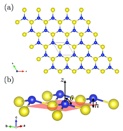
Using first-principle calculations, Ciraci et al. investigated two-dimensional honeycomb structures of group-IV elements and their binary compounds as well as the compounds of group III-V elementsŞahin et al. (2009). It was found that buckled AB monolayers with trigonal symmetry (e.g., group IV binary monolayers SiGe, SiSn, GeSn and group III-V binary monolayers AlSb, GaP, GaAs, InP, InAs, InSb) Şahin et al. (2009), in which a trigonal sublattice of A ions is separated from that of B ions (Fig. 1a), are more stable with respect to a planar geometry. The tendency to a buckled geometry was explained in terms of the destabilization of the bonds in hybridization due to the increase of the bond length between the two atoms A and B, as it happens in silicene and germanene compared to graphene.Ezawa (2013) As a result of the buckling, the states dehybridize and the ,, orbitals combine with orbitals to form new -like orbitals. Three of these states form covalent bonds with three nearest-neighbor atoms, while one -like orbital directed upward perpendicular to the atomic plane forms a weak bond with the adjacent -like orbital directed downward. Interestingly, silicene and germanene are expected to display valley-contrasting properties analogous to graphene as soon as the inversion symmetry is broken, e.g., by applying an external electric field.Ezawa (2013) Therefore, other buckled honeycomb lattices are expected to display similar valley-dependent properties. Furthermore, in buckled trigonal structure, one can introduce a sublattice pseudospin describing the binary layer DOFXu et al. (2014): the pseudospin up (down) refers to the state where the charge carrier is located in the upper (lower) layer, or equivalently in the A (B) sublattice. Therefore, a pseudospin polarization would directly correspond to an electrical polarization. In fact, buckled AB monolayers have no inversion symmetry and actually belong to the polar space group , with the polar axis perpendicular to the layer (Fig. 1b), possibly leading to a ferroelectric (FE) state; in addition to the emergence of valley-contrasting physics, therefore, they can also display a Rashba effectRashba (1960), which would likely be coupled to and controllable with the FE polarization. If this is the case, it would be possible to act on the spin DOFs of these valley-active systems by reversing the FE polarization of the monolayer Di Sante et al. (2013). We explore this possibility in the present work, where we theoretically predict, by density functional calculations complemented with model Hamiltonian analysis, that the buckled group IV and group III-V binary monolayers with trigonal symmetryŞahin et al. (2009) are 2D ferroelectrics with spin-valley coupling and Rashba effects in their electronic structure. We show that SOC and a bipartite honeycomb lattice with different A and B atoms are at the origin of a spin-valley-sublattice coupling which is responsible for a valley-dependent Zeeman-like splitting at the K and -K valleys, while a nonvanishing buckling is responsible for an in-plane Rashba spin-texture that is controllable by electric field.
From the experimental point of view, several top-down and bottom-up methods have been proposed and devised for synthesizing 2D materials, as reported in recent review papersButler et al. (2013); Balendhran et al. (2014). Specifically, both silicene and germanene have been proven to exist as a monolayer when grown on selected metal substrates. Although bulk Si cannot form a layered phase like graphite, experiments of surface-assisted epitaxial growth show the presence of nanoribbons of silicene on Ag(110)Aufray et al. (2010) and 2D monolayers with buckled honeycomb structure on Ag(111)Vogt et al. (2012); Feng et al. (2012) and Ir(111)Meng et al. (2013). Similarly, successful attempts to grow 2D germanium sheets with a honeycomb structure on a platinum(111) and gold(111) template have been reported very recentlyLi et al. (2014); Dávila et al. (2014). As for binary compounds, to the best of our knowledge, no other 2D monolayers beside boron nitride have been synthesized yetMiró et al. (2014), even though almost 2D nanoflakes of SiC with thickness of the order of 1 nm have been obtained by means of solution-based exfoliation of SiC crystalsLin (2012). We hope that our work can stimulate further experimental work to fill this gap.
II METHODS
Our density functional calculations for buckled AB monolayers were carried out using the projector augmented wave (PAW) method implemented in VASP using the PBEsol functional Blöchl (1994); Kresse and Furthmüller (1996); Perdew et al. (1996). -electrons are included in the valence in the PAW potentials. Test calculations were also performed using the Heyd-Scuseria-Ernzerhof (HSE) screened hybrid density functional Heyd et al. (2003). The atom positions were optimized until the residual forces were smaller than 0.001 eV/Å with the plane-wave cutoff energy of 500 eV and a set of 881 k-points for the irreducible BZ. Repeated image interactions were made negligible by including a vacuum layer of 26 Å in the simulations. The FE polarization is calculated using the Berry’s phase method King-Smith and Vanderbilt (1993), and SOC is self consistently taken into account.
The first-principle Berry curvature is calculated according to the usual linear response Kubo-like formula
| (1) |
where is the Fermi distribution function, is the velocity operator, and is the lattice-periodic eigenvector with eigenvalue of the Fourier transformed Wannier Hamiltonian as calculated by projecting the DFT Hamiltonian onto a Wannier basis Mostofi et al. (2008).
III RESULTS
Starting from the buckled compounds listed in ref.15 we have calculated the buckling heights h (Å), band gaps Eg (eV), barrier heights Ea (eV per formula unit) estimated as the energy difference between the FE buckled structure and the paraelectric planar one, FE polarizations P () and spin-splittings () (in meV) at the K point for valence (conduction) bands, see Table 1. In this work, we follow previous theoretical studiesŞahin et al. (2009) and assume that atoms A and B belong to the ordered bipartite lattice shown in Fig. 1a), i.e., we neglect the role of disorderDi Sante et al. (2014) ; indeed this effect would require a separate analysis, beyond the purpose of the present study. First we note that if A, B atoms belong to the same group (i.e., IV group), the A-B bond is polar due to the electronegativity difference between A and B, since the electronegativity within a given family of elements decreases on going from the top to a lower period. On the other hand, when A, B atoms belongs to III and V group, respectively, the electronegativity difference becomes even more pronounced (the electronegativity increasing from left to right along the period). The trigonal symmetry and the buckled honeycomb structure imply a local uniaxial dipole moment along the 3-fold rotation axis. By analogy with the Ising model for uniaxial ferromagnets, which is well known to display a phase transition even in the two-dimensional latticeOnsager (1944), a FE phase transition is indeed possible, where the two symmetry-equivalent energy minima with opposite polarity are obtained by reversing the buckling angle. The estimated FE polarizations of the group IV binary AB monolayers are significantly large, with calculated typical values of the order of 1-4 while the group III-V binary AB monolayers have a larger FE polarization, because of the larger electronegativity difference and larger dipole moment carried by each A-B bond. Typical values in this case are around 10 . It is interesting to note that the calculated values for the estimated FE polarizations are always one order of magnitude larger than those measured in 2D freely-suspended FE smectic-C filmsRosenblatt et al. (1979) and nematic monolayersTabe et al. (2003), showing . Evaluation of Born effective charges confirms the estimated values of FE polarization, at the same time providing an estimate of the depolarization field, which is expected to significantly affect the FE properties of thin films. In fact, the electrostatic energy of the depolarization field is proportional to the the square of and inversely proportional to the electronic polarizability of the material; since the latter is almost constant for all the considered systems, i.e. , while is significantly small (for the component of the charge tensor we calculate for group IV and for group III-V binary AB monolayers), the depolarization field can be expected to be weaker than that preventing ferroelectricity in ultrathin films of ferroelectric perovskites, supporting the feasibility of stable FE distortions. Eventually, the energy barriers Ea calculated for the ABBA conversion are comparable with those estimated for conventional FE oxides, such as PbTiO3 for which Eformula unit, as well as with that of the recently predicted 1 FE phase of MoS2 Shirodkar and Waghmare (2014), suggesting that the polarization reversal could be experimentally accessible. Inelastic electron excitations from a STM tip could be also used to switch between the two FE phases, as recently proposed for bistable molecular switchesFu et al. (2010); Pavliček et al. (2012).
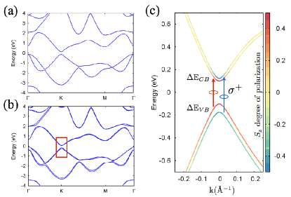
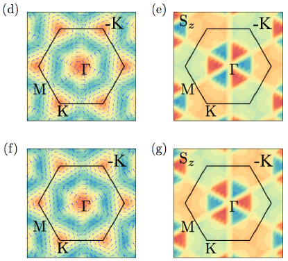
We discuss then the electronic band structures of a representative example, GeSn, calculated without and with SOC and shown in Fig. 2 (a-b). Band structures for all the other compounds are displayed in the Supplementary Material. The band gap opens at the K point, where both the valence (VB) and conduction (CB) bands are split by SOC, as highlighted in Fig. 2(c). It is also clear from Fig. 2(c) that electrons around the K valley feel a strong Zeeman-like magnetic field, which is responsible for a valley-dependent out-of-plane spin polarization both in the VB and in the CB Yuan et al. (2013). The same holds for the -K valley. Due to the time-reversal symmetry, the system remains overall non-magnetic, with opposite out-of-plane spin polarization at time-reversed K and -K points, as clearly shown in Fig. 2 (e),(g). Therefore, the considered buckled FE monolayers show coupled spin and valley physics, thus possibly allowing the spin and valley control similar to layered transition metal dichalcogenides. As for MoS2 and other group-VI dichalcogenides, the valley Hall effect should be accompanied by a spin Hall effect for both the electron and hole-doped systems, whose robustness can be deduced by the expected long relaxation time of spin and valley indicesXiao et al. (2012a). Because of the spin-valley coupling and the valley-contrasting spin splittings and , the energy conservation would imply a simultaneous flipping of spin and valley indices; since two adjacent valleys are separated by a wave vector comparable with the size of the Brillouin zone, such simultaneous flipping would require atomic scale (magnetic) scatterers. In the absence of such scatterers, both holes and electrons are expected to display long spin and valley lifetimes, therefore allowing robust Hall effects around both the valence and conduction-band edges Xiao et al. (2012a). The spin textures of the two spin-split VBs calculated for the whole BZ are presented in Fig. 2 (d-g). The typical Rashba spin patterns are clearly observed around K and -K valleys, with the in-plane spin components rotating clockwise or counterclockwise in spin-split bands, as shown in Fig. 2 (d),(f) for upper and lower VBs. Interestingly, while the out-of-plane spin components show opposite polarizations at time-reversed valleys, the in-plane spin components display the same chirality at K and -K points in a single VB; both the Rashba-like chirality and the valley-dependent magnetic moments appear then to be reversed in the other spin-split VB. A similar behaviour is found in the spin-split CBs, while the VB maximum (VBM) and CB minimum (CBM) show same chiralities and out-of-plane polarization direction. When the FE polarization is switched by reversing the buckling, the in-plane spin-texture chiralities are fully reversed, suggesting the possibilities to control the Rashba effect by exploiting the FE properties of binary monolayers. On the other hand, the out-of-plane spin polarization remains exactly the same in opposite FE states. Interestingly, the valley-dependent spin polarization survives even when the buckling is completely suppressed as in the flat graphene-like structure, as a consequence of the non-centrosymmetric, albeit nonpolar, character of the planar honeycomb structure with binary composition.
To understand the origin of this exotic spin and valley physics, and its interplay with the intrinsic FE polarization in buckled trigonal monolayers, we now investigate the microscopic mechanisms underlying the low-energy properties around the Fermi level at the K and -K valleys. In the absence of buckling () and SOC, the low-energy effective Hamiltonian around the K point describing low-energy states with mainly character reads
| (2) |
where is the sublattice pseudospin trasforming like Pauli matrices, is a valley index for points, is the Fermi velocity, and the first ”mass” term originates from the different ions located in A and B sublattices. Contrary to the case of graphene, silicene and other group-IV binary monolayers Castro Neto et al. (2009); Konschuh et al. (2010); Liu et al. (2011); Drummond et al. (2012), the additional mass term leads to an intrinsic gap in the energy spectrum, which opens at the Dirac point (the effective parameters are estimated in a tight-binding framework and given in the Supplementary Material). The VBs and CBs remain spin-degenerate, as sketched in Fig. 3(a) for VBs. When SOC is turned on in the planar structure (), additional terms appear in the effective Hamiltonian (2), namely
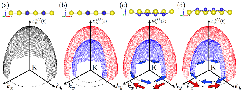
| (3) |
where are effective material-dependent parameters arising from the interplay of atomic SOC constants , local orbital energies and hopping integrals , and , which in turn depend on geometrical factors such as the buckling angle (see Supplementary Material). The presence of SOC, therefore, introduces an effective Zeeman-like valley-dependent magnetic field , which removes the spin-degeneracy without mixing spin up and spin down states, leading to spin-split VBs and CBs with energies and a net out-of-plane spin polarizations at the K valleys, as sketched in Fig. 3(b). The VB and CB spin-splittings are listed in Fig. 1 for all considered binary monolayers, and shown in Fig. 2(c) for the representative case of GeSn. Additionally, the mass term acquires a spin-valley-sublattice contribution which indeed guarantees the coupling between the spin and valley physics. Interestingly, the additional coupling terms experienced by a given sublattice originate from the atomic SOC of the other sublattice mediated by the hopping interactions — in fact, carriers in the A sublattice feel the atomic SOC of B ions through the term , and vice versa. This is reflected in the different size of spin-splitting gaps in VBs and CBS. As shown in Fig. 2(c) for the representative case of GeSn, the spin-splitting is larger at VBs rather than at CBs, despite the fact that VBs and CBs show predominant Ge and Sn characters, respectively, as a consequence of the larger electronegativity of Ge. Naïvely, one would expect a larger spin-splitting at CBs than at VBs, since the atomic SOC constant of Sn is larger than that of Ge, .Wittel and Manne (1974) Indeed, the opposite is observed, since carriers with a predominant Ge character experience the SOC-induced interaction coming from the Sn ions, and vice versa. The same holds for all other compounds, as can be inferred looking at values reported in Table 1. It is important to stress that such spin-splitting effects arise uniquely from the binary composition of the monolayers, implying . The spin-valley coupling, emerging already in the planar noncentrosymmetric binary monolayer, is therefore independent of the buckling distortion; in fact, the are even functions of the buckling angle , implying that valley-constrating properties such as the out-of-plane spin polarization are not expected to qualitatively change under FE distortions. Furthermore, since the valley-dependent coupling terms do not mix the spin-up and spin-down components, remains a good quantum number, analogously to what happens in MoS2 monolayers.
One can easily evaluate the Berry curvature of the Bloch electrons, associated with the valley and spin Hall effect:
| (4) |
where the sign refers to CB and VB, respectively, as well as the coupling strength with optical fields of circular polarization:
| (5) |
which display the same form found for MoS2 monolayers, leading to similar expectations about the robustness of (valley and spin) Hall physics and optoelectronic effectsXiao et al. (2012a). In particular, the Berry curvature shows opposite sign in different valleys, while the interband optical transitions are found to be uniquely coupled with () circularly polarized optical field at the K (-K) valley, the valley optical selection rules being also spin-dependent as shown in Fig. 2 (c). It is also clear from Eqs. (4), (5) that the strength of such spin-valley physics is mainly governed by the spin-valley-sublattice coupling parametrized by , even though the valley-contrasting spin splitting of both VBs and CBs is due to the effective magnetic field .
When ferroelectricity sets in, lowering the trigonal symmetry from to and leading to a finite buckling , an intrinsic Rashba term must be added in the effective Hamiltonian Eq. (3), namely:
| (6) |
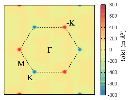
where and is a complex material-dependent parameter which is odd under the switching of the buckling angle (see Supplementary Material). This Rashba coupling term gives rise to in-plane circularly rotating spin-texture around each K valley, with opposite chiralities at spin-split VBs (CBs) as shown in Fig. 3(c)), while substantially not affecting the out-of-plane spin polarization. Neglecting for the sake of simplicity, the expectation value for in-plane spin polarizations reads and for the VBM and CBM (the overall chirality being fully reversed in the VBM-1 and CBM+1 branches), i.e., the typical Rashba-like behaviour, which appears to be valley-independent, in agreement with our DFT calculations. Since is an odd function of the buckling angle with respect to planar structure , the buckling reversal, i.e., the switching of the ferroelectric polarization, leads to a complete reversal of the in-plane Rashba spin-texture chirality only, while the VBs and CBs preserve their out-of-plane spin-polarization, as schematically shown in Fig. 3(c-d). This behaviour perfectly agrees with our first-principles calculations, since its origin lies in the opposite -dependence of spin-valley () and intrinsic Rashba () coupling constants at, and around, the K point (note that only when and the k-vector differs from K Liu et al. (2011)). It is worthwhile to notice that, although the Rashba-like coupling term causes a mixing of spin-up and spin-down states, the valley physics appears to be robust to buckling distortion. In fact, the Berry curvature has been evaluated from first-principles for the representative GeSn with buckled honeycomb structure, and it has been found to display opposite sign at K and -K valleys, as shown in Fig. 4.
IV CONCLUSIONS
Our first-principles calculations predict a spontaneous FE polarization in buckled group IV and group III-V binary monolayers with trigonal symmetry. Unlike the case of graphene, silicene, germanene and other single atomic type monolayers, the presence of a diatomic basis that breaks the inversion symmetry — even in the planar geometry — leads to the emergence of Zeeman-like spin-split bands with coupled spin-valley physics analogous to the MoS2 case. At the same time, it is mainly responsible for the onset of the FE phase when the honeycomb lattice buckles, allowing for an electrically controllable Rashba-like spin-texture around the K valleys, whose chirality is locked to the polarization direction and therefore fully reversible upon FE switching. Such Rashba split bands can be effectively detected by spin-resolved spectroscopic techniques, and the process of hole and electron injection allows for the engineering of two dimensional spin field-effect-transistors (FETs) Di Sante et al. (2013). Even though the spin-valley and Rashba phenomenologies appear to be substantially decoupled, our work suggests a route towards the integration of valleytronic and spintronic features in FE multivalley materials, opening unforeseen possibility in the exciting world of spintronics. Currently the growth of these 2D monolayers on a suitable substrate is difficult, and the effect of the substrate has been only recently addressed Singh et al. (2014). Nevertheless, it is highly desirable to find ways of preparing these fascinating 2D monolayers.
V ACKNOWLEDGMENTS
Figures are plotted using VESTA and Gnuplot packages. The authors are thankful to the HPC Center of NCSU for computing resources. A.S. acknowledges support from CNR Short Term Mobility program prot. AMMCNT-CNR0026336 for the visiting stay at IFW Leibniz Institute, Dresden, Germany where this project was conceived and started.
References
- Rycerz et al. (2007) A. Rycerz, J. Tworzydo, and C. W. J. Beenakker, Valley filter and valley valve in graphene, Nat. Phys. 3, 172 (2007).
- Xiao et al. (2007) D. Xiao, W. Yao, and Q. Niu, Valley-contrasting physics in graphene: Magnetic moment and topological transport, Phys. Rev. Lett. 99, 236809 (2007).
- Castro Neto et al. (2009) A. H. Castro Neto, F. Guinea, N. M. R. Peres, K. S. Novoselov, and A. K. Geim, The electronic properties of graphene, Rev. Mod. Phys. 81, 109 (2009).
- Lee et al. (2012) M.-K. Lee, N.-Y. Lue, C.-K. Wen, and G. Y. Wu, Valley-based field-effect transistors in graphene, Phys. Rev. B 86, 165411 (2012).
- Zeng et al. (2012) H. Zeng, J. Dai, W. Yao, D. Xiao, and X. Cui, Valley polarization in MoS2 monolayers by optical pumping, Nat. Nanotech. 7, 490 (2012).
- Mak et al. (2012) K. F. Mak, K. He, J. Shan, and T. F. Heinz, Control of valley polarization in monolayer MoS2 by optical helicity, Nat. Nanotech. 7, 494 (2012).
- Cao et al. (2012) T. Cao, G. Wang, W. Han, H. Ye, C. Zhu, J. Shi, Q. Niu, P. Tan, E. Wang, B. Liu, et al., Valley-selective circular dichroism of monolayer molybdenum disulphide, Nat. Commun. 3, 887 (2012).
- Behnia (2012) K. Behnia, Condensed-matter physics: Polarized light boosts valleytronics, Nat. Nanotech. 7, 488 (2012).
- Yuan et al. (2013) H. Yuan, M. S. Bahramy, K. Morimoto, S. Wu, K. Nomura, B.-J. Yang, H. Shimotani, R. Suzuki, M. Toh, C. Kloc, et al., Zeeman-type spin splitting controlled by an electric field, Nat. Phys. 9, 563 (2013).
- Mai et al. (2014) C. Mai, A. Barrette, Y. Yu, Y. G. Semenov, K. W. Kim, L. Cao, and K. Gundogdu, Many-body effects in valleytronics: Direct measurement of valley lifetimes in single-layer MoS2, Nano Letters 14, 202 (2014).
- Mak et al. (2014) K. F. Mak, K. L. McGill, J. Park, and P. L. McEuen, The valley hall effect in MoS2 transistors, Science 344, 1489 (2014).
- Xu et al. (2014) X. Xu, W. Yao, D. Xiao, and T. F. Heinz, Spin and pseudospins in layered transition metal dichalcogenides, Nat. Phys. 10, 343 (2014).
- Xiao et al. (2012a) D. Xiao, G.-B. Liu, W. Feng, X. Xu, and W. Yao, Coupled spin and valley physics in monolayers of and other group-VI dichalcogenides, Phys. Rev. Lett. 108, 196802 (2012a).
- Xiao et al. (2012b) D. Xiao, G.-B. Liu, W. Feng, X. Xu, and W. Yao, Coupled spin and valley physics in monolayers of MoS2 and other group-VI dichalcogenides, Phys. Rev. Lett. 108, 196802 (2012b).
- Şahin et al. (2009) H. Şahin, S. Cahangirov, M. Topsakal, E. Bekaroglu, E. Akturk, R. T. Senger, and S. Ciraci, Monolayer honeycomb structures of group-IV elements and III-V binary compounds: First-principles calculations, Phys. Rev. B 80, 155453 (2009).
- Ezawa (2013) M. Ezawa, Spin valleytronics in silicene: Quantum spin hall-quantum anomalous hall insulators and single-valley semimetals, Phys. Rev. B 87, 155415 (2013).
- Rashba (1960) E. I. Rashba, Properties of semiconductors with an extremum loop. 1. cyclotron and combinational resonance in a magnetic field perpendicular to the plane of the loop, Sov. Phys. Solid State 2, 1109 (1960).
- Di Sante et al. (2013) D. Di Sante, P. Barone, R. Bertacco, and S. Picozzi, Electric control of the giant rashba effect in bulk GeTe, Advanced Materials 25, 509 (2013), ISSN 1521-4095.
- Butler et al. (2013) S. Z. Butler, S. M. Hollen, L. Cao, Y. Cui, J. A. Gupta, H. R. GutiÈrrez, T. F. Heinz, S. S. Hong, J. Huang, A. F. Ismach, et al., Progress, challenges, and opportunities in two-dimensional materials beyond graphene, ACS Nano 7, 2898 (2013).
- Balendhran et al. (2014) S. Balendhran, S. Walia, H. Nili, S. Sriram, and M. Bhaskaran, Elemental analogues of graphene: Silicene, germanene, stanene, and phosphorene, Small (2014).
- Aufray et al. (2010) B. Aufray, A. Kara, S. Vizzini, H. Oughaddou, C. Leandri, B. Ealet, and G. Le Lay, Graphene-like silicon nanoribbons on ag(110): A possible formation of silicene, Appl. Phys. Lett. 96, 183102 (2010).
- Vogt et al. (2012) P. Vogt, P. De Padova, C. Quaresima, J. Avila, E. Frantzeskakis, M. C. Asensio, A. Resta, B. Ealet, and G. L. Lay, Silicene: Compelling experimental evidence for graphenelike two-dimensional silicon, Phys. Rev. Lett. 108, 155501 (2012).
- Feng et al. (2012) B. J. Feng, Z. J. Ding, S. Meng, Y. Yao, X. He, P. Cheng, L. Chen, and H. Wu, Evidence of silicene in honeycomb structures of silicon on ag(111), Nano Lett. 12, 3507 (2012).
- Meng et al. (2013) L. Meng, Y. Wang, L. Zhang, S. Du, R. Wu, L. Li, Y. Zhang, G. Li, H. Zhou, W. A. Hofer, et al., Buckled silicene formation on ir(111), Nano Letters 13, 685 (2013).
- Li et al. (2014) L. Li, S.-Z. Lu, J. Pan, Z. Qin, Y.-Q. Wang, Y. Wang, G.-Y. Cao, S. Du, and H.-J. Gao, Buckled germanene formation on Pt(111), Advanced Materials 26, 4820 (2014).
- Dávila et al. (2014) M. E. Dávila, L. Xian, S. Cahangirov, A. Rubio, and G. Le Lay, Germanene: a novel two-dimensional germanium allotrope akin to graphene and silicene, New Journal of Physics 16, 095002 (2014).
- Miró et al. (2014) P. Miró, M. Audiffred, and T. Heine, An atlas of two-dimensional materials, Chem. Soc. Rev. 43, 6537 (2014).
- Lin (2012) S. S. J. Lin, Previous Article Next Article Table of Contents Light-Emitting Two-Dimensional Ultrathin Silicon Carbide, Phys. Chem. C 116, 3951 (2012).
- Blöchl (1994) P. E. Blöchl, Projector augmented-wave method, Phys. Rev. B 50, 17953 (1994).
- Kresse and Furthmüller (1996) G. Kresse and J. Furthmüller, Efficient iterative schemes for ab initio total-energy calculations using a plane-wave basis set, Phys. Rev. B 54, 11169 (1996).
- Perdew et al. (1996) J. P. Perdew, K. Burke, and M. Ernzerhof, Generalized gradient approximation made simple, Phys. Rev. Lett. 77, 3865 (1996).
- Heyd et al. (2003) J. Heyd, G. E. Scuseria, and M. Ernzerhof, Hybrid functionals based on a screened coulomb potential, The Journal of Chemical Physics 118, 8207 (2003).
- King-Smith and Vanderbilt (1993) R. D. King-Smith and D. Vanderbilt, Theory of polarization of crystalline solids, Phys. Rev. B 47, 1651 (1993).
- Mostofi et al. (2008) A. A. Mostofi, J. R. Yates, Y.-S. Lee, I. Souza, D. Vanderbilt, and N. Marzari, Wannier90: A tool for obtaining maximally-localised wannier functions, Comput. Phys. Commun. 178, 685 (2008).
- Di Sante et al. (2014) D. Di Sante, P. Barone, E. Plekhanov, S. Ciuchi, and S. Picozzi, Robustness against Disorder of Relativistic Spectral Properties in Chalcogenide Alloys, arxiv:1407.2064, (2014).
- Onsager (1944) L. Onsager, Crystal Statistics. I. A Two-Dimensional Model with an Order-Disorder Transition, Phys. Rev. 65, 117 (1944).
- Rosenblatt et al. (1979) C. Rosenblatt, R. Pindak, N. Clark, and R. Meyer, Freely suspended ferroelectric liquid-crystal films: Absolute measurements of polarization, elastic constants, and viscosities, Phys. Rev. Lett. 42, 1220 (1979).
- Tabe et al. (2003) Y. Tabe, T. Yamamoto, I. Nishiyama, M. Yoneya, and H. Yokoyama, Ferroelectric nematic monolayer, Jpn. J. Appl. Phys. 42, L406 (2003).
- Shirodkar and Waghmare (2014) S. N. Shirodkar and U. V. Waghmare, Emergence of ferroelectricity at a metal-semiconductor transition in a monolayer of , Phys. Rev. Lett. 112, 157601 (2014).
- Fu et al. (2010) Q. Fu, Y. Luo, J. Yang, and J. Hou, Understanding the concept of randomness in inelastic electron tunneling excitations, Phys. Chem. Chem. Phys. 12, 12012 (2010).
- Pavliček et al. (2012) N. Pavliček, B. Fleury, M. Neu, J. Niedenführ, C. Herranz-Lancho, M. Ruben, and J. Repp, Atomic force microscopy reveals bistable configurations of dibenzo[a,h]thianthrene and their interconversion pathway, Phys. Rev. Lett. 108, 086101 (2012).
- Konschuh et al. (2010) S. Konschuh, M. Gmitra, and J. Fabian, Tight-binding theory of the spin-orbit coupling in graphene, Phys. Rev. B 82, 245412 (2010).
- Liu et al. (2011) C.-C. Liu, H. Jiang, and Y. Yao, Low-energy effective hamiltonian involving spin-orbit coupling in silicene and two-dimensional germanium and tin, Phys. Rev. B 84, 195430 (2011).
- Drummond et al. (2012) N. D. Drummond, V. Zólyomi, and V. I. Fal’ko, Electrically tunable band gap in silicene, Phys. Rev. B 85, 075423 (2012).
- Wittel and Manne (1974) K. Wittel and R. Manne, Atomic spin-orbit interaction parameters from spectral data for 19 elements, Theoret. Chim. Acta (Berl.) 33, 347 (1974).
- Singh et al. (2014) A. K. Singh, H. L. Zhuang, and R. G. Hennig, Ab initio synthesis of single-layer III-V materials, Phys. Rev. B 89, 245431 (2014).