Intrinsic surface dipole in topological insulators
Abstract
We calculate the local density of states of two prototypical topological insulators (Bi2Se3 and Bi2Te2Se) as a function of distance from the surface within density functional theory. We find that, in the absence of disorder or doping, there is a 2 nm thick surface dipole the origin of which is the occupation of the topological surface states above the Dirac point. As a consequence, the bottom of the conduction band is bent upward by about 75 meV near the surface, and there is a hump-like feature associated with the top of the valence band. We expect that band bending will occur in all pristine topological insulators as long as the Fermi level does not cross the Dirac point. Our results show that topological insulators are intrinsic Schottky barrier solar cells.
pacs:
73.20.At,73.30.+y,71.20.-b,77.90.+k,73.50.-h, 73.61.-rI Introduction
Semiconductor interfaces are of fundamental importance in electronic device operation. At the heart of this technology are heterojunctions made of n-doped and p-doped semiconductorsMönch (2010). The charge carriers through -junctions can be accurately controlled via gate voltages, giving diodes and transistors its useful properties. It is well known that near the interface region there is a permanent electric field, which bends the conduction and valence levels. This region is referred to as space-charge region or interface dipole (surface dipole if the interface is with vacuum). This band-bending (BB) effect is also of fundamental importance in silicon-based solar cell technology, where the electric field separates photo-exited electrons and holes.
Band bending in semiconductors can be determined from the I-V characteristics of the junction, from surface photo-voltage spectroscopyKronik and Shapira (1999), surface potential microscopy or from Angle-Resolved Photoemission Spectroscopy (ARPES). Many factors contribute to the BB measured by any of these techniques. Among the most important are the difference in work functions of the materials at the interface, the image charge potential and possible interface reconstruction. These are ‘intrinsic’ contributions. Occupied impurity states also contribute to BB (extrinsic contributions). Analytical calculations of BB in semiconductor interfaces usually determine the charge distribution self-consistently from an effective one-dimensional Poisson equation and a single-particle Schrodinger equation. Such calculations often depend on unknown parameters, which are ultimately determined in experiments.
Recently, a new type of ‘semiconductor’ was discovered, the topological insulator (TI), which is an insulator in the bulk but has metallic surface states (SSs) protected by time reversal symmetryRoy (2009); Moore and Balents (2007); Fu and Kane (2007); Dzero et al. (2010); Zhang et al. (2013). For further details about TIs we refer the reader to the many excellent reviews of the subject such as Ref. Hasan and Moore, 2011 and references therein. At low energies, the surface states of TIs can be described by the Dirac equation in two-dimensions with the spin of the electron locked to its momentum. This property can be utilized in spintronicYokoyama and Murakami (2014) applications.
Band bending in TIs surfaces has been investigated experimentally with ARPES Hsieh et al. (2009); Bianchi et al. (2010); Analytis et al. (2010); Chen et al. (1012); Neupane et al. (2012); Edmonds et al. (2014); Frantzeskakis et al. (2015); Urazhdin et al. (2004) and other techniquesPettes et al. (2013); Narayan et al. (2014). However, the results have not been consistent, even in apparently similar conditions. For example, BB of Bi2Se3 has been found to be either upward (75 meV)Analytis et al. (2010) or downward (100–300 meV)Hsieh et al. (2009); Bianchi et al. (2010); Chen et al. (1012); ViolBarbosa et al. (2013); Frantzeskakis et al. (2015); Urazhdin et al. (2004). This suggest that the dominant contribution to BB in these experiments is extrinsic, e.g., doping, and hence it is very sensitive to the details of the sample preparation. In view of these considerations, it is clear that extrinsic and intrinsic effects play a role in actual experiments and that disentangling intrinsic from extrinsic factors would be very useful as a benchmark for future experimental and theoretical studies. On the theoretical side, the Poisson-Schrodinger equationsKing et al. (2008); Brahlek et al. (2015) and tight-binding modelsGalanakis and Stanescu (2012); Bahramy et al. (2012) have been successfully used to model BB in TIs. However, understanding and characterizing BB in TIs interfaces has not been explored systematically from first principles despite the fact that it could open the door for new technological applications, e.g., in solar cell technology.
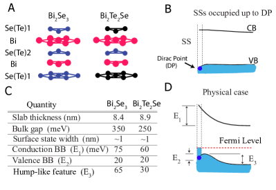
In this paper we resolve the intrinsic contribution to BB (and hence to the surface dipole) by studying BB in pristine TIs Bi2Se3 and Bi2Te2Se. We consider a finite slab of Bi2Se3 and Bi2Te2Se and calculate variations of the local density of states (LDOS) as a function of depth using first principles density functional theory (DFT) with no fitting parameters. Fig. 1 summarizes our main results. We find an upward BB of the conduction and valence bands within 2 nm below the surface. The upward BB for Bi2Se3 and Bi2Te2Se is 75 meV and 60 meV respectively, even without disorder or doping. We attribute this BB to the occupation of topological SSs above the Dirac point. In the valence band we find a hump-like feature near the surface consisting of an upward bend (65 meV for Bi2Se3 and 30 meV for Bi2Te2Se) 2 nm from the surface, followed by a 20 meV downward bend 1 nm from the surface. We note that, our results do not rely on the Poisson equation to find the equilibrium charge distribution. Instead, the charge distribution arises from the inclusion of electron correlations at the DFT level. Therefore, we expect deviations from Poisson electrostatics. In particular, we find asymmetric BB of the valence and conduction bands, including a small downward BB of the valence band near the surface. Finally, although we used Bi2Se3 and Bi2Te2Se as TI prototypes, we expect similar order of magnitude BB for the family Bi2X3 with X=Se,Te and X2Te2Y with X=Sb,Bi and Y=S,Se, as Y and X enter with the same oxidation state.
This paper is organized as follows. In Sec. II we compute the band structure and LDOS of Bi2Se3 and Bi2Te2Se for the physically relevant situation where thermalized electrons fill the SSs above the Dirac point. In Sec. III we compare with the LDOS without spin-orbit coupling and with SSs occupied up to the DP and discuss the origin of the surface dipole. The appendix A contains additional information about the calculation.
II Local density of states
II.1 Crystal structure
Bi2Se3 and Bi2Te2Se are layered materials with rhombohedral (Rm) crystal structureCava et al. (2013). The structure can be represented as hexagonal planes stacked along the -axis containing only one type of atom, as shown in Fig. 1A. In one hexagonal unit cell, the order of the stacking is -[Se(2)-Bi-Se(1)-Bi-Se(2)]0-[Se(2)-Bi-Se(1)-Bi-Se(2)]1/3-[Se(2)-Bi-Se(1)-Bi-Se(2)]2/3 in Bi2Se3 and -[Te-Bi-Se-Bi-Te]0-[Te-Bi-Se-Bi-Te]1/3-[Te-Bi-Se-Bi-Te]2/3- in Bi2Te2Se. The group of five atomic layers in square brackets are often referred to as a quintuple layer (QL) shown in Fig. 1A. The subscripts indicate the fractional translation of the QL along the -axis of the hexagonal unit cell. The QLs are weakly coupled by Van der Waals forces, forming natural cleavage planes with negligible surface reconstruction. In what follows we present results for Bi2Se3 only, the results for Bi2Te2Se are similar and summarized in Fig. 1.
II.2 Band structure and local density of states
Here we provide some details of our first-principles calculation of the LDOS (more information is in the appendix A). We used Quantum-ESPRESSOGiannozzi et al. (2009) and Wannier90Mostofi et al. (2008) to compute the band structures and LDOS of Bi2Se3. Our periodic computational unit cell consists of 9 QLs of Bi2Se3 (total width of 8.4 nm) with a 1 nm of vacuum layer between periodic images. Therefore, each computational cell consists of 45 atoms in total, at which the LDOS is calculated. Bi2Se3 slabs are terminated with Se atoms on both sides, as found in experimentsCava et al. (2013). Other terminations are possible but generally lead to reconstructed surfaces which are absent in our case.
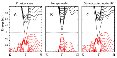
To visualize BB we compute the LDOS across the entire slab and then note its variations in intensity as a function of depth. To obtain the LDOS with a required energy resolution we use the Wannier interpolationYates et al. (2007) method. This method consists of first computing Kohn-Sham orbitals and energies on a coarsely sampled Brillouin zone (we used a uniform 99 mesh) for electronic bands of interest. In Fig. 2A we show the band structure of Bi2Se3. The Dirac point (DP) is at the point of the Brillouin zone 180 meV below the Fermi level. Note that the SSs (above the DP) are occupied. and there is a bulk gap of meV consistent with previous reportsBlack et al. (1957); Xia et al. (2009); Xu et al. ; Lovett (1977). We then use these orbitals to construct localized Wannier functionsMarzari et al. (2012) centered at lattice vector , with both like atomic character for all 45 layers in the slab (index goes from 1 to 45). Since the Hamiltonian is exponentially localized in the Wannier basis we can use this basis to interpolate electronic orbitals and energies on a very dense k-mesh (30003000) with a negligible additional computational cost. Finally, we obtain the LDOS from the histogram of the interpolated electronic energies ,
| (1) |
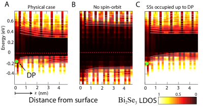
Here the sum is calculated over all electronic states (band and momentum ), and over all Wannier functions (), so that the local density of states depends only on atomic layer () and energy (). The LDOS (shown in Fig. 3A) was projected at each of the 45 atomic layers of our supercell. The horizontal axes indicates the approximate distance from the left surface. The matrix element appearing in the sum is independent of lattice vector , since the Bloch functions are cell-periodic. Therefore we can sum only over for simplicity.
Fig. 3A shows the LDOS across a slab of Bi2Se3 in the physically relevant case with thermalized electrons occupying the SSs. For comparison we also include the case without spin-orbit coupling (B) and with occupied SSs up to the DP only in (C). In this section we discuss the physically relevant case Fig. 3A. The discussion of cases without spin orbit coupling and with partial filling of SSs is given in Sec. III.1 and Sec. III.2.
Near the surface there is a non-zero spectral weight extending roughly nm into the bulk, which originates from the topological SSs. Interestingly, one can follow the edges of the valence and conduction bands by observing how the spectral weight intensity varies across the slab. To quantify BB we follow the following procedure. We define BB by the maximal deviation of the LDOS isocontours (see white lines in Fig. 3A) between the first and middle QLs in a given energy window (200 meV below the valence band maximum or above the conduction band minimum). With this definition, the edge of the conduction band bends upward by meV within 2 nm of the surface, Fig. 3A. On the other hand, the valence band has a hump-like feature near the surface consisting of a 65 meV upward bend 2 nm from the surface followed by a 20 meV downward bend 1 nm from the surface.
III Surface dipole
In this Section we study the origin of BB in Bi2Se3 and show that it can be modeled as a macroscopic surface dipoleMönch (2010). We will study both the effect of the spin-orbit interaction and the population of the surface states.
III.1 Spin-obit interaction
Turning off the spin-orbit interaction in our calculation reduces the TI to a non-topological insulator, with no topological SSs. This can be seen by the lack of edge states in Fig. 2B. We expect that with no topological SS, the charge distribution across the slab will be affected. This is indeed what we find, see Fig. 3B. Without spin-orbit interaction, the conduction band is nearly flat. The maximum bending is less than 20 meV. Therefore, we can assign the origin of the upward band bending of the conduction band to the presence of the topological SSs. We focus on the occupation of these states in more detail in the next subsection.
Focusing now on the valence band, we find that even without spin-orbit coupling there is a 75 meV downward BB and a much smaller hump-like feature. Therefore, we again assign the origin of the upward BB to the presence of topological SSs.
III.2 Population of the surface states
While the presence of topological SSs is essential for BB in pristine TI slabs, here we discuss the importance of their filling. As discussed in Sec. II, the DP of the Bi2Se3 slab is below the Fermi level, and hence some of the SSs which are above the DP are populated, Fig. 2A. Since the whole slab is neutral, this excess charge on the surface must be compensated by a partial depopulation of some of the bulk-like states.
Fig. 3C shows the LDOS for a Bi2Se3 slab with SSs occupied up to the Dirac point only and unoccupied above it, see also Fig. 2C. This can be accomplished by setting the population of the first 252 valence bands at all k-points to unity. As can be seen, most of the upward BB features disappear. The conduction BB is only 20 meV across the slab. For the valence band, maximal upward bending (within 200 meV of the valence band maximum) is only 15 meV. However, a downward bend of the valence band near the surface is still present. The downward bend is 90 meV, even larger than in the thermalized case.
Therefore, to conclude this and the previous subsection, we find that upward bending of the conduction and valence bands is present only when topological SSs are present (Sec. II.1) and when they are occupied.
III.3 Magnitude of the surface dipole
As a consistency check we compare the surface charge density estimated in two ways. First, we calculate the phase space occupied by the SSs from the DP up to the Fermi level in our thermalized calculation. This estimate gives us a surface charge density cm-2. Second, we estimate the surface charge density by modeling the region near the surface as an electric double layer separated by about nm with opposite charges. One layer is negative due to the occupation of the SS and the other is positive from the depletion of electrons in the bulk-like region. In Fig. 3b, we see that the potential discontinuity at the surface is meV and from (with the permittivity of Bi2Se3 Madelung et al. (1998)) we obtain C/m. Using we find a surface density cm-2 in a reasonable agreement with the first estimate, thus confirming that the occupation of SS above the DP is responsible for the observed band bending.
IV Conclusion
We have shown that free surfaces of pristine Bi2Se3 and Bi2Te2Se with no doping or disorder have an intrinsic surface dipole. Bi2Se3 and Bi2Te2Se grown without any post-processing tend to be doped and disordered and appear to be good bulk conductorsRen et al. (2010); Bianchi et al. (2010); Neupane et al. (2012); Yang et al. (2012); Marcinkova et al. (2013); Brahlek et al. (2015); Arita et al. (2014). However, even in this case the upward contribution to band bending computed in this work is present. We note that Ref. Analytis et al. (2010) finds 75 meV upward band bending in Bi2Se3 which is similar to pristine Bi2Se3. However, more analysis is required to attribute this band bending solely to intrinsic effects. As samples become cleanerHoefera et al. (2014) only the intrinsic component computed here will remain. We comment that, we have considered the case where the DP lies below the Fermi level. We leave for future work the discussion of the case where the Fermi level crosses at or below the DP.
Importantly, the intrinsic band bending found in this work means that TIs generate up to 75 meV of surface photvoltageKronik and Shapira (1999) upon illumination. The same principle applies in the operation of Schottky barrier solar cells, where the interface dipole is created at a metal-semiconductor interface. Therefore, TIs could operate as intrinsic Schottky barrier solar cells with an estimated maximum efficiency of 7% according to the Shockley-QueisserMönch (2010) criterion.
After completion of this work we became aware of Ref. Rakyta et al., which considers BB in Bi2Se3.
V Acknowledgments
We thank J. Moore, J. Analytis, M. L. Cohen, C. Salazar, C. Ojeda-Aristizabal, and A. Drieschova for useful discussions. Support was provided by Conacyt and NSF DMR-1206513, and Computer resources by NERSC under Contract No. DE-AC02-05CH11231.
Appendix A Numerical details
We use density functional theory (DFT) as implemented in the Quantum-ESPRESSOGiannozzi et al. (2009) computer package with the generalized gradient approximationPerdew et al. (1997) to the exchange-correlation energy functional. Convergence of the energy in the self-consistent iterations was verified to better than 10-8 Ry and we used a 100 Ry plane wave kinetic energy cutoff. A k-point mesh of 991 (999) was used in slab (bulk) calculations. We performed a fully-relativistic calculation with relativistic effects included in the pseudopotentials.
We first fully relax the lattice constants and the internal coordinates in bulk compounds. For Bi2Se3 we obtained the DFT optimized parameters Å, Å and for Bi2Te2Se Å, Å. Following a bulk structural relaxation we performed the relaxation of the internal coordinates in the slab geometry. We checked that the LDOS results did not change if we used 6 QL instead of 9 QL or if we used 20 Å vacuum instead of 10 Å. We then constructed maximally localized Wannier functionsMarzari et al. (2012) and performed the Wannier interpolationYates et al. (2007) using the Wannier90Mostofi et al. (2008) computer package. For initial projections we used and -like atom-centered orbitals for both Bi and Se (Te) atoms.
In the non-thermal calculation discussed in section III.2, the occupations of the lowest bands at each k-point are fixed to one, where is the total pseudocharge of our unit-cell (=252). Filling up the lowest bands in a topological insulator corresponds to occupying states up to the Dirac point.
References
- Mönch (2010) W. Mönch, Semiconductor Surfaces and Interfaces (Springer, 2010).
- Kronik and Shapira (1999) L. Kronik and Y. Shapira, Surf. Sci. Rep. 37, 1 (1999).
- Roy (2009) R. Roy, Phys. Rev. B 79, 195322 (2009).
- Moore and Balents (2007) J. E. Moore and L. Balents, Phys. Rev. B 75, 121306 (2007).
- Fu and Kane (2007) L. Fu and C. L. Kane, Phys. Rev. B 76, 045302 (2007).
- Dzero et al. (2010) M. Dzero, K. Sun, V. Galitski, and P. Coleman, Phys. Rev. Lett. 104, 106408 (2010).
- Zhang et al. (2013) X. Zhang, N. P. Butch, P. Syers, S. Ziemak, R. L. Greene, and J. Paglione, Phys. Rev. X 3, 011011 (2013).
- Hasan and Moore (2011) M. Z. Hasan and J. E. Moore, Annu. Rev. Condens. Matter Phys. 2, 55 (2011).
- Yokoyama and Murakami (2014) T. Yokoyama and S. Murakami, Physica E: Low-dimensional Systems and Nanostructures 55, 1 (2014).
- Hsieh et al. (2009) D. Hsieh, Y. Xia, D. Qian, L. Wray, J. H. Dil, F. Meier, J. Osterwalder, L. Patthey, J. G. Checkelsky, N. P. Ong, A. V. Fedorov, H. Lin, A. Bansil, D. Grauer, Y. S. Hor, R. J. Cava, and M. Z. Hasan, Nature 460, 1101 (2009).
- Bianchi et al. (2010) M. Bianchi, D. Guan, S. Bao, J. Mi, B. B. Iversen, P. D. King, and P. Hofmann, Nat Commun 1, 128 (2010).
- Analytis et al. (2010) J. G. Analytis, J.-H. Chu, Y. Chen, F. Corredor, R. D. McDonald, Z. X. Shen, and I. R. Fisher, Phys. Rev. B 81, 205407 (2010).
- Chen et al. (1012) C. Chen, S. He, H. Weng, W. Zhang, L. Zhao, H. Liu, X. Jia, D. Mou, S. Liu, J. He, Y. Peng, Y. Feng, Z. Xie, G. Liu, X. Dong, J. Zhang, X. Wang, Q. Peng, Z. Wang, S. Zhang, F. Yang, C. Chen, Z. Xu, X. Dai, Z. Fang, and X. J. Zhou, Proc. Natl. Acad. Sci. USA 109, 3694 (1012).
- Neupane et al. (2012) M. Neupane, S.-Y. Xu, L. A. Wray, A. Petersen, R. Shankar, N. Alidoust, C. Liu, A. Fedorov, H. Ji, J. M. Allred, Y. S. Hor, T.-R. Chang, H.-T. Jeng, H. Lin, A. Bansil, R. J. Cava, and M. Z. Hasan, Phys. Rev. 85, 235406 (2012).
- Edmonds et al. (2014) M. T. Edmonds, J. T. Hellerstedt, A. Tadich, A. Schenk, K. M. O’Donnell, J. Tosado, N. P. Butch, P. Syers, J. Paglione, and M. S. Fuhrer, The Journal of Physical Chemistry C 118, 20413 (2014).
- Frantzeskakis et al. (2015) E. Frantzeskakis, N. de Jong, B. Zwartsenberg, T. V. Bay, Y. K. Huang, S. V. Ramankutty, A. Tytarenko, D. Wu, Y. Pan, S. Hollanders, M. Radovic, N. C. Plumb, N. Xu, M. Shi, C. Lupulescu, T. Arion, R. Ovsyannikov, A. Varykhalov, W. Eberhardt, A. de Visser, E. van Heumen, and M. S. Golden, Phys. Rev. B 91, 205134 (2015).
- Urazhdin et al. (2004) S. Urazhdin, D. Bilc, S. D. Mahanti, S. H. Tessmer, T. Kyratsi, and M. G. Kanatzidis, Phys. Rev. B 69, 085313 (2004).
- Pettes et al. (2013) M. T. Pettes, J. Maassen, I. Jo, M. S. Lundstrom, and L. Shi, Nano Letters 13, 5316 (2013).
- Narayan et al. (2014) A. Narayan, I. Rungger, A. Droghetti, and S. Sanvito, Phys. Rev. B 90, 205431 (2014).
- ViolBarbosa et al. (2013) C. E. ViolBarbosa, C. Shekhar, B. Yan, S. Ouardi, E. Ikenaga, G. H. Fecher, and C. Felser, Phys. Rev. B 88, 195128 (2013).
- King et al. (2008) P. D. C. King, T. D. Veal, and C. F. McConville, Phys. Rev. B 77, 125305 (2008).
- Brahlek et al. (2015) M. Brahlek, N. Koirala, N. Bansal, and S. Oh, Solid State Communications 215, 54 (2015).
- Galanakis and Stanescu (2012) D. Galanakis and T. D. Stanescu, Phys. Rev. B 86, 195311 (2012).
- Bahramy et al. (2012) M. Bahramy, P. King, A. de la Torre, J. Chang, M. Shi, L. Patthey, G. Balakrishnan, P. Hofmann, R. Arita, N. Nagaosa, and F. Baumberger, Nat Commun 3, 1159 (2012).
- Cava et al. (2013) R. J. Cava, H. Ji, M. K. Fuccillo, Q. D. Gibson, and Y. S. Horb, J. Mater. Chem. C 1, 3176 (2013).
- Giannozzi et al. (2009) P. Giannozzi et al., Journal of Physics: Condensed Matter 21, 395502 (2009).
- Mostofi et al. (2008) A. A. Mostofi, J. R. Yates, Y.-S. Lee, I. Souza, D. Vanderbilt, and N. Marzari, Comput. Phys. Commun. 178, 685 (2008).
- Yates et al. (2007) J. Yates, X. Wang, D. Vanderbilt, and I. Souza, Phys. Rev. B 75, 195121 (2007).
- Black et al. (1957) J. Black, E. Conwell, L. Seigle, and C. Spencer, Journal of Physics and Chemistry of Solids 2, 240 (1957).
- Xia et al. (2009) Y. Xia, D. Qian, D. Hsieh, L. Wray, A. Pal, H. Lin, A. Bansil, D. Grauer, Y. S. Hor, R. J. Cava, and M. Z. Hasan, Nat. Phys. 5, 398 (2009).
- (31) S.-Y. Xu, L. A. Wray, Y. Xia, R. Shankar, A. Petersen, A. Fedorov, H. Lin, A. Bansil, Y. S. Hor, D. Grauer, R. J. Cava, and M. Z. Hasan, “Discovery of several large families of topological insulator classes with backscattering-suppressed spin-polarized single-dirac-cone on the surface,” ArXiv:1007.5111 [cond-mat.mes-hall].
- Lovett (1977) D. Lovett, Semimetals and Narrow-bandgap Semiconductors (Pion Limited, London, UK, 1977).
- Marzari et al. (2012) N. Marzari, A. A. Mostofi, J. R. Yates, I. Souza, and D. Vanderbilt, Rev. Mod. Phys. 84, 1419 (2012).
- Madelung et al. (1998) O. Madelung, U. Rössler, and M. Schulz, eds., Non-Tetrahedrally Bonded Elements and Binary Compounds I (Springer, Berlin, 1998).
- Ren et al. (2010) Z. Ren, A. A. Taskin, S. Sasaki, K. Segawa, and Y. Ando, Phys. Rev. B 82, 241306 (2010).
- Yang et al. (2012) K. Yang, W. Setyawan, S. Wang, M. Buongiorno Nardelli, and S. Curtarolo, Nat Mater 11, 614 (2012).
- Marcinkova et al. (2013) A. Marcinkova, J. K. Wang, C. Slavonic, A. H. Nevidomskyy, K. F. Kelly, Y. Filinchuk, and E. Morosan, Phys. Rev. B 88, 165128 (2013).
- Arita et al. (2014) M. Arita, H. Sato, K. Shimada, H. Namatame, M. Taniguchi, M. Sasaki, M. Kitaura, A. Ohnishi, and H.-J. Kim, JPS Conf. Proc. 1, 012017 (2014).
- Hoefera et al. (2014) K. Hoefera, C. Beckera, D. Rata, J. Swanson, P. Thalmeiera, and L. H. Tjenga, Proc. Natl. Acad. Sci. USA 111, 14979 (2014).
- (40) P. Rakyta, B. Ujfalussy, and L. Szunyogh, “Band bending at the surface of bi2se3 studied from first principles,” ArXiv:1504.05071 [cond-mat.mes-hall].
- Perdew et al. (1997) J. P. Perdew, K. Burke, and M. Ernzerhof, Phys. Rev. Lett. 78, 1396 (1997).