‡ Department of Physics, Oregon State University, Corvallis, OR, 97330, USA
Domain Decomposition for Heterojunction Problems in Semiconductors
Abstract
We present a domain decomposition approach for the simulation of charge transport in heterojunction semiconductors. The problem is characterized by a large variation of primary variables across an interface region of a size much smaller than the device scale, and requires a multiscale approach in which that region is modeled as an internal boundary. The model combines drift diffusion equations on subdomains coupled by thermionic emission heterojunction model on the interface which involves a nonhomogeneous jump computed at fine scale with Density Functional Theory. Our full domain decomposition approach extends our previous work for the potential equation only, and we present perspectives on its HPC implementation. The model can be used, e.g., for the design of higher efficiency solar cells for which experimental results are not available. More generally, our algorithm is naturally parallelizable and is a new domain decomposition paradigm for problems with multiscale phenomena associated with internal interfaces and/or boundary layers.
Keywords:
Domain Decomposition, Drift-Diffusion Equations, Density Functional Theory, Heterojunction, Multiscale Semiconductor Modeling, Solar Cells.1 Introduction
In this paper we present a multiscale approach for heterojunction interfaces in semiconductors, part of a larger interdisciplinary effort between computational mathematicians, physicists, and material scientists interested in building more efficient solar cells. The higher efficiency (may) arise from putting together different semiconductor materials, i.e., creating a heterojunction.
The computational challenge is that phenomena at heterojunctions must be resolved at the angstrom scale while the size of the device is on the scale of microns, thus it is difficult to simultaneously account for correct physics and keep the model computationally tractable. To model charge transport at the device scale we use the drift diffusion (D-D) system [14]. For interfaces, we follow the approach from [9] in which the interface region is shrunk to a low-dimensional internal boundary, and physics at this interface is approximated by the thermionic emission model (TEM) which consists of unusual internal boundary conditions with jumps.
We determine the data for these jumps from an angstrom scale calculation using Density Functional Theory (DFT), and we model the physics away from the interface by the usual (D-D) equations coupled by TEM. The D-D model can be hard-coded as a monolithic approach which appears intractable and/or impractical in 2d/3d with complicated interface geometries. Our proposed alternative is to apply a domain decomposition (DDM) approach which allows the use of “black box” D-D solvers in subdomains, and enforces the TEM conditions at the level of the DDM driver. DDM have been applied to D-D, e.g., in [12, 13], where the focus was on a multicore HPC implementation of efficiently implemented suite of linear and nonlinear solvers. Here we align the DDM with handling microscale physics at material interfaces. More importantly, fully decoupling the subdomains is a first step towards a true multiscale simulation where the behavior in the heterojunction region is treated simultaneously by a computational method at microscale.
The DDM approach we propose is non-standard because of the nonhomogeneous jumps arising from TEM. In [7] we presented the DDP algorithm for the potential equation. In this paper we report on the next nontrivial step which involves carrier transport equations. Here the interface model is an unusual Robin-like interface equation. The algorithm DDC works well and has promising properties.
This paper consists of the following. In Section 2 we describe the model. In Section 3 we present our domain decomposition algorithms, and in Section 4 we present numerical results for the simulation of two semiconductor heterojunctions. Finally in Section 5 we present conclusions, HPC context, and describe future work.
2 Computational Model for Coupled Scales
The continuum D-D model with TEM is described first, followed by the angstrom scale DFT model.
2.1 Device scale continuum models: drift diffusion (D-D) system
Let , , be an open connected set with a Lipschitz boundary . Let , , be two non-overlapping subsets of s.t. , , and denote . We assume is a - dimensional manifold, and . Each subdomain corresponds to a distinct semiconductor material, and the interface between them. We adopt the following usual notation: , , and denotes the jump of .
In the bulk semiconductor domains , , the charge transport is described by the D-D system: a potential equation solved for electrostatic potential , and two continuity equations solved for the Slotboom variables and ; these relate to the electron and hole densities and , respectively, via . (The scaling parameters and depend on the material and the doping profile). We recall that in Slotboom variables the continuity equations are self-adjoint [14]. The stationary D-D model is
| (2) | |||||
| (3) |
For background on the D-D model the reader is referred to [1, 10, 14, 15, 19, 20]. In (2)–(3) we use data: the net doping profile , a given expression for the electron-hole pair generation and recombination , electrical permittivity , and electron and hole diffusivities , . Also, is another scaling parameter [7].
The model (2)–(3) is completed with external boundary conditions; we impose Dirichlet conditions for the potential and recombination-velocity (Robin type) conditions for electron and hole densities. To this we add the TEM transmission conditions on the interface [9]
| (5) | |||||
| (9) | |||||
Here and are the electron and hole currents
| (10) | |||
| (11) |
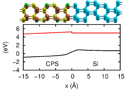
Also, and are constants dependent on material properties and temperature, and is a jump discontinuity in the electrostatic potential. These can be determined by a DFT calculation, see Figure 1 for illustration.

2.2 Density Functional Theory for Atomic Scale
Heterojunction parameters in (5)–(9) are determined by quantum mechanics of electrons. The Schrödinger equation solved for wave function is fundamental for quantum behavior, but the problem of interacting electrons is computationally intractable for large .
DFT [5, 4] provides an efficient method of determining material properties from first principles by shifting focus from wave functions to electron density, . The density sought in DFT is a function in , while the Schrödinger equation is solved for . Finding is possible via application of the theory of Hohenberg and Kohn to a minimization problem in , and is equivalent to the solution of the Schrödinger equation for the ground state. However, an energy functional needed in the minimization principle in DFT is unknown, and DFT requires approximations to . The Kohn-Sham equations provide a basis for these approximations, and their solution can be found iteratively [5, 4].
DFT is a widely used, low cost, first principles method which solves the zero temperature, zero current ground state of a system [5, 4]. The local pseudopotential calculated by DFT is continuous at an interface (see Figure 1), and can be used with known material properties to obtain the change in the continuous electrostatic potential occurring close to a heterojunction. The potential jump (offset) is a ground state property of the heterojunction structure, and DFT solution in the heterojunction region provides the data needed for TEM.
3 Domain Decomposition for Continuum Model
The procedure to solve (2)–(9) numerically is a set of nested iterations, with three levels of nesting.
First, when solving (2)–(9), we employ the usual Gummel Map [18, 10], an iterative decoupling technique within which we solve each component equation of (2)–(3) independently. Note that each equation is still nonlinear in its primary variable, thus we must use Newton’s iteration.
Furthermore, each component equation employs DDM independently to resolve the corresponding part of TEM. In particular, we solve potential equation (2) with (5), the electron transport (2) with (9), and the hole transport (3) with (9). The DDM we use is an iterative substructuring method designed as a Richardson scheme [17] to resolve the TEM, defined and executed independently for each component. In what follows is an acceleration parameter, different for each component equation. Since the DDM algorithm for equation is entirely analogous to that for equation, we only define the latter.
Last, each subdomain solve of the DDM is nonlinear, and we use Newton-Raphson iteration to resolve this.
3.1 Domain Decomposition for Potential Equation (2), (5)
3.2 Domain Decomposition for Continuity Equation (2), (9)
Here we seek to find data so that (2), (9) is equivalent to the problem:
| (14) | |||||
| (16) | |||||
which requires the homogeneous jump condition .
Algorithm DDC proposed in this paper is very different from DDP because it proceeds sequentially from domain to domain . In addition, while it corrects in a manner similar to a Neumann-Neumann algorithm, in (16) it takes advantage of Neumann data from resulting from (14). An appropriate parallel algorithm for DDC which uses Neumann rather than Dirichlet data as in (14), (16) was promising for a synthetic example, but it has difficulties with convergence for realistic devices.
While DDP and DDC are motivated by the multiphysics nature of the model, they may be viewed as extensions of Neumann-Neumann iterative substructuring methods to nonhomogeneous jumps and Robin-like transmission conditions. A scalable parallel implementation may be achieved in the future using two-level techniques [[17] §3.3.2].
4 Heterojunction Semiconductor Simulation
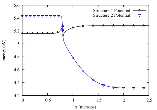
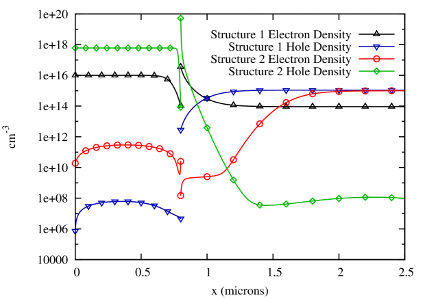
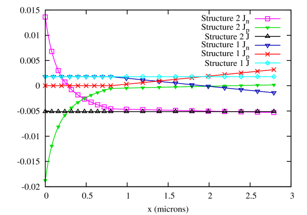
Now we present numerical simulation results. Structure 1 is synthetic and solar cell-like, and is made of two hypothetical materials we call L1 and R1. Structure 2 is made of Si and Cu3PSe4 (CPS). In Table 2 we give details.
We use DFT to calculate eV for the Cu0.75P0.25-Si interface formed from CPS (001) and the Si (111) surfaces having normally oriented dangling bonds. Next we apply Domain Decomposition and specifically the algorithms DDP, DDC; see Figure 2. For both structures we see the impact of heterojunction and large jumps of across the interface. The results are validated with a hard-coded monolithic solver.
As concerns solver’s performance, in Table 1 we show that DDC is mesh independent, similarly to DDP [7]. Furthermore, the choice of is crucial. (In forthcoming work [3] we show how is determined from analysis of the jump data.)
| DDC u, | DDC v, | |||||||
|---|---|---|---|---|---|---|---|---|
| N | GI 1 | GI 2 | GI 3 | GI 4 | GI 1 | GI 2 | GI 3 | GI 4 |
| 201 | 6 | 2 | 1 | 1 | 5 | 3 | 1 | 1 |
| 401 | 5 | 2 | 1 | 1 | 8 | 4 | 1 | 1 |
| 601 | 3 | 2 | 1 | 1 | 8 | 4 | 1 | 1 |
| 801 | 4 | 2 | 1 | 1 | 8 | 4 | 1 | 1 |
| property | L1 | R1 | CPS | Si |
| permittivity | 10.0 | 10.0 | 15.1 [6] | 11.9 [21] |
| electron affinity (eV) | 5 | 5 | 4.05 | 4.05 [21] |
| band gap (eV) | 1.0 | 0.5 | 1.4 [6] | 1.12 [21] |
| eff. electron density of states (cm-3) | ||||
| eff. hole density of states (cm-3) | ||||
| dopant charge density (cm-3) | [6] | |||
| electron diffusion constant (cm2/s) | 2.0 | 2.0 | 2.6 | 37.6 [21] |
| hole diffusion constant (cm2/s) | 1.0 | 1.0 | 0.5 | 12.9 [21] |
| constant photogeneration density (cm-3/s) | ||||
| direct recombination constant (cm3/s) | ||||
| jump in potential (eV) | -0.15 | -0.01 | ||
5 Conclusions
The main contribution reported in this paper advances HPC methodology for solving problems with complex interface physics. We presented DDM for the simulation of charge transport in heterojunction semiconductors. Our method allows the coupling of “black-box” D-D (drift diffusion) solvers in subdomains corresponding to single semiconductor materials. We compared DDM to a monolithic solver, and the results are promising; see Table 3. As usual, DDM approach wins for large . Also, it works when monolithic solver fails. In the model presented here DFT is used to determine heterojunction parameters but is currently entirely decoupled from D-D solvers in the bulk subdomains. Our approach is a first step towards a true multiscale simulation coupling the atomic and device scales.
| Monolithic time (sec) | DDM time (sec) | DDM parallel estimate | Current | |
|---|---|---|---|---|
| 501/501 | 0.5494 | 1.313 | 0.8 | 0.006637 |
| 751/751 | 0.8122 | 1.4537 | 0.9 | 0.006649 |
| 1001/1001 | 1.0231 | 1.4173 | 0.9 | 0.006655 |
| 1251/1251 | failed | 2.1665 | 1.3 | 0.0066592 |
At the current stage, the computational complexities of the microscale and macroscale simulations are vastly different. The microscale DFT simulations using VASP solver [11] for electronic structure simulations running on 4 machines with 12 cores with MPI2, take several days to complete. On the other hand, the D-D solver takes less than minutes at worst to complete; see Table 3. Thus, a true coupled multiscale approach is not feasible yet.
More broadly, problems with nonhomogeneous jump conditions across interfaces only begin to be investigated from mathematical and computational point of view. Our DDM approach is a new paradigm that applies elsewhere, e.g., for discrete fracture approximation models where nonhomogeneous jump conditions arise [8, 16].
Acknowledgements: This research was partially supported by the grant NSF-DMS 1035513 grant “SOLAR: Enhanced Photovoltaic Efficiency through Heterojunction assisted Impact Ionization.” We would like to thank G. Schneider for useful discussions.
References
- [1] R. E. Bank, D. J. Rose, and W. Fichtner, Numerical methods for semiconductor device simulation, Siam J. Sci. Statist. Comput., 1983.
- [2] K. Chang and D. Kwak, Discontinuous bubble scheme for elliptic problems with jumps in the solution, Comp. Meth. in Applied Mech. and Eng., (2011).
- [3] T. Costa, D. H. Foster, M. Peszynska, Progress in modeling of semiconductor structures with heterojunctions, submitted, (2014).
- [4] E. Engel and R. M. Dreizler, Density functional theory: An advanced course, Springer, 2011.
- [5] C. Fiolhais, F. Nogueira, and M. A. Marques, A primer in density functional theory, Springer, (2003).
- [6] D. H. Foster, F. L. Barras, J. M. Vielma, and G. Schneider, Defect physics and electronic properties of Cu3PSe4 from first principles, Phys. Rev. B, (2013).
- [7] D. H. Foster, T. Costa, M. Peszynska, and G. Schneider, Multiscale modeling of solar cells with interface phenomena, Journal Coupled Systems and Multiscale Dynamics, (2013).
- [8] N. Frih, J. E. Roberts, and A. Saada, Modeling fractures as interfaces: A model for Forchheimer fractures, Comput. Geosci., 2008.
- [9] K. Horio and H. Yanai, Numerical modeling of heterojunctions including the thermionic emission mechanism at the heterojunction interface, IEEE Trans. Electron Devices, (1990).
- [10] J. W. Jerome, Analysis of charge transport, Springer-Verlag, Berlin, 1996, A mathematical study of semiconductor devices.
- [11] G. Kresse and J. Furthmüller, Efficient iterative schemes for ab initio total-energy calculations using a plane-wave basis set, Phys. Rev. B, (1996).
- [12] P. Lin, J. Shadid, M. Sala, R. Tuminaro, G. Hennigan and R. Hoekstra, Performance of a parallel algebraic multilevel preconditioner for stabilized finite element semiconductor device modeling, Journal of Computational Physics, (2009).
- [13] P. Lin and J. Shadid, Towards large-scale multi-socket, multicore parallel simulations: Performance of an MPI-only semiconductor device simulator, Journal of Computational Physics, (2010).
- [14] P. A. Markowich, The stationary semiconductor device equations, Computational Microelectronics, Springer-Verlag, Vienna, 1986.
- [15] P. A. Markowich, C. A. Ringhofer, and C. Schmeiser, Semiconductor Equations, Springer-Verlag, Vienna, 1990.
- [16] V. Martin, J. Jaffré, and J. E. Roberts, Modeling fractures and barriers as interfaces for flow in porous media, SISC, (2005).
- [17] A. Quarteroni and A. Valli, Domain decomposition methods for partial differential equations, Oxford, 1999.
- [18] R. Sacco, C. de Falco, and J. Jerome, Quantum-corrected drift-diffusion models: Solution fixed point map and finite element approximation, J. Comput. Phys. (2009).
- [19] K. Seeger, Semiconductor Physics: An Introduction, Springer, Berlin 2010.
- [20] S. Selberherr, Analysis and simulation of semiconductor devices, Springer-Verlag, 1984.
- [21] S. Sze and K. Ng, Physics of semiconductor devices, Wiley-Interscience, 2006.