Domain wall of a ferromagnet on a three-dimensional topological insulator
Abstract
Topological insulators (TIs) show rich phenomena and functions which can never be realized in ordinary insulators. Most of them come from the peculiar surface or edge states. Especially, the quantized anomalous Hall effect (QAHE) without an external magnetic field is realized in the two-dimensional ferromagnet on a three-dimensional TI which supports the dissipationless edge current. Here we demonstrate theoretically that the domain wall of this ferromagnet, which carries edge current, is charged and can be controlled by the external electric field. The chirality and relative stability of the Neel wall and Bloch wall depend on the position of the Fermi energy as well as the form of the coupling between the magnetic moments and orbital of the host TI. These findings will pave a path to utilize the magnets on TI for the spintronics applications.
The dissipationless topological currents (TIs) are the issue of current great interests. TIs and superconductors are the two representative materials which support the dissipationless currents on their surface TI1 ; TI2 . These materials are characterized by the gapped bulk states and gapless surface or edge states due to bulk–edge or bulk–surface correspondence. The surface Weyl states of a three-dimensional (3D) TI offer an arena for various novel physical properties due to its momentum–spin locking, as described by the two-dimensional (2D) Hamiltonian,
| (1) |
where is the normal unit vector to the surface, are the Pauli matrices, and is the 2D momentum. The sign differs for the top and bottom surfaces.
This surface state shows various unique properties when magnetic moments are coupled to it. For example, the effect of the doped magnetic moments on the transport properties has been studied theoretically FCZhang . Another remarkable phenomena is the quantized anomalous Hall effect (QAHE), where the Hall conductance is quantized with the vanishing longitudinal conductance without the external magnetic field Haldane ; Onoda ; Yu ; Nomura ; Abanin . When the exchange coupling to the magnetization is introduced, the Hamiltonian reads
| (2) |
where is the exchange energy, and is the direction of the magnetization. When the magnetization is normal to the surface, i.e., , the the mass gap opens in the surface state and half-quantized Hall conductance , i.e., the quantized anomalous Hall effect (QAHE) is realized, when the Fermi energy is tuned within in this mass gap. Note that the observed Hall conductance is the sum of the upper and bottom surfaces and hence .
The dynamics of the magnetization on 3D TI has been also studied theoretically based on the 2D Weyl Hamiltonian Franz ; Yokoyama ; Loss ; Linder ; Ferreiros ; Baum ; Mendler ; Hurst . Experimentally, the gap opening in the surface states of a 3D TI Bi2Se3 due to the doping of magnetic ions has been observed by angle-resolved photoemission spectroscopy (ARPES) Chen . Also the QAHE has been recently observed in Bi2Te3 with Cr doping Zhang ; Chang ; Joe ; Chang2 ; Bestwick ; Kou ; Figuerou; Ni . When the magnetization is along the direction both for the top and bottom surfaces, the edge channel goes along the side surface. The edge channel appears also along the domain wall which separates the two domains of and .
In the field of spintronics, the magnetic domain walls play important roles as the information carriers and their manipulation is a keen issue. Especially, the racetrack memory using the current-driven motion of the domain wall is proposed Parkin1 . Recently, the vital role of the spin–orbit interaction (SOI) in the domain wall motion has been revealed Parkin2 . The spin-to-charge conversion by the SOI is also a hot topic in spintronics Fert . Therefore, it is an important issue to examine theoretically the domain walls in the ferromagnet on a TI from the viewpoint of the spintronics, since the momentum–spin locking at the surface state of the TI corresponds to the strong-coupling limit of the SOI.
There are some subtle issues in the Hamiltonian Eq. (2): (i) One needs to introduce the energy cut off to avoid the ultra-violet divergence, which is naturally given by the band gap of the 3D bulk states; namely, the surface states merge into the bulk conduction and valence bands. However, when the in-plane components of the magnetization are finite, the 2D momentum shifts, and the surface states near the merging points are changed, which contribute to the energy but can not be properly described by Eq. (2). (ii) The exchange coupling to the magnetization in Eq. (2) needs to be re-examined. The Cr atoms replaces Bi atoms, and can have the exchange coupling to the -orbitals of both Bi and Te, but with different weight. This changes the effective Hamiltonian for the surface state. (iii) The dependence on the depth of the magnetic layer, and the relation between the top and bottom surfaces are of interest as well, which is accessed only by the 3D model with finite thickness.
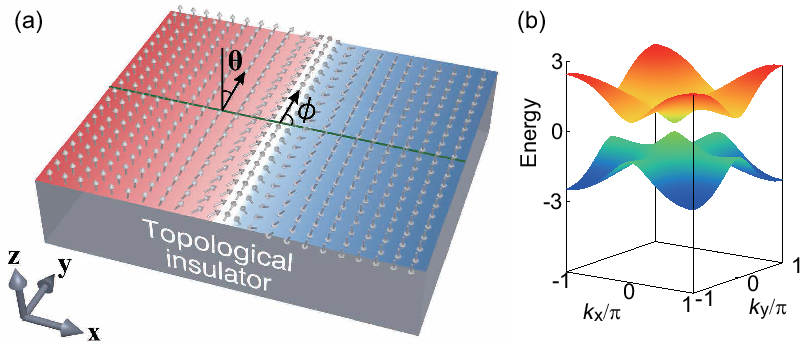
In this paper, we investigate the stability and charging effects of a domain wall on the surface of the 3D TI based on the 3D tight-binding model. We carry out a numerical study based on the 3D tight-binding model Liu ; Shan ; ZhangH . We also perform an analytical study based on the effective 2D surface Hamiltonian which we derive from the 3D model. The exchange coupling is found to be anisotropic due to the orbital dependence, as we have mentioned. Figure 1 shows the schematic structure of the domain wall on a TI. The angle determines the structure of the domain wall, i.e., Neel or Bloch wall and its chirality. It is found that the most stable domain wall structure depends on the position of the Fermi energy, i.e., one can control the domain structure by gating. Another important result is that the domain wall is charged due to the two effects: One originates in the zero-energy edge state along the domain wall and the other in the charging effect of the magnetic texture. It will offer a way to manipulate the domain wall by electric field.
Results
Model Hamiltonian. We start with the following minimum model for 3D TIs Liu ; ZhangH ,
| (3) |
where is the Fermi velocity, and are the mass parameters. For the numerical calculation, we use the corresponding lattice model Liu ; Shan ; ZhangH ,
| (4) |
where is the transfer integral, and are the Pauli matrices for the spin and pseudospin degrees of freedom, and
| (5) |
The pseudospin represents the -orbitals of the Bi and Te. We have introduced an orbital-dependent exchange interaction, i.e., the orbital is coupled with , while the orbital with . When , the exchange interactions exist only at one orbital, while equally coupled when . In the case of Cr doped (Bi,Sb)2Te3, the magnetization is induced by the substitution of the (Bi,Sb) atoms by the Cr atoms, which is coupled mostly to the Te atoms. Hence it is expected that Henk . Therefore, we consider the two limiting cases of and . The case is useful since it provides us with a clear physical picture from the analytical point of view.
The system without the magnetism is known Liu ; Shan ; ZhangH to be a strong TI for and , a weak TI for , and the trivial insulator for and . The strong TI phase is the most intriguing, and hence we choose , and for numerical calculations and for illustration throughout the paper. The bulk gap is given by . Note that even the tight-binding Hamiltonian Eq. (4) is an effective one around the top of the valence band and the bottom of the conduction band. In actual materials, there are many other bands which contribute to the higher energy and short wavelength physics. Therefore, we regard the “lattice constant” (which is put to be unity) as the coarse grained one.
We are interested in the low-energy physics on the surface of the above TI. We consider a slab geometry with finite thickness along the direction. Then, the 2D Weyl fermions appear both on the top and bottom surfaces. This can be seen from the 2D low-energy Hamiltonian by projecting the 3D continuum Hamiltonian (3) onto the space spanned by the surface states. The result is
| (6) |
with the parameters and , which are related with and in Eq. (3) and (4). It can be derived as follows.
At the point, we obtain the surface states by solving the eigenequation (3) without the exchange terms by setting and for the semi-infinite system. The top and bottom surface states are represented as
| (7) |
where in the part corresponds to the top and bottom surface respectively, and represents the spin eigenvalue. Therefore, we find
| (8) |
It follows that , namely the exchange term in the 3D bulk Hamiltonian is projected into the Ising interaction in the 2D surface Hamiltonian. For the orbital-dependent exchange term, the components are
| (9) |
It follows that , namely the orbital-dependent exchange term in the 3D bulk Hamiltonian is projected into the in-plane exchange term in the 2D surface Hamiltonian.
Our important observation is that the exchange interaction on the 2D surface is anisotropic even if that in the 3D bulk is isotropic. The perpendicular exchange interaction is induced by the -term while the in-plane exchange interaction is induced by the -term.
In what follows we carry out an analysis of the surface states of the TI numerically based on the 3D Hamiltonian Eq. (4) and analytically based on the 2D Hamiltonian Eq. (6). The momentum is a good quantum number since the surface are assumed to be uniform in the direction. We numerically diagonalize the system with sites along the direction and sites along the direction for each . We take points for . We set two domain walls to apply the periodic boundary condition for direction, and we illustrate figures for one of the domain walls throughout the paper.
Magnetic domain wall. We consider a magnetic domain wall between the two degenerate ground states, lying along the axis on the surface of the TI,
| (10) |
with . The angle represents the type of magnetic domain wall. Especially, represent the Neel walls, while the Bloch walls,
| (11) |
We call () as Neel 1 (Neel 2), and as Bloch. These two types of Bloch walls are related by the mirror symmetry operation with respect to the plane.
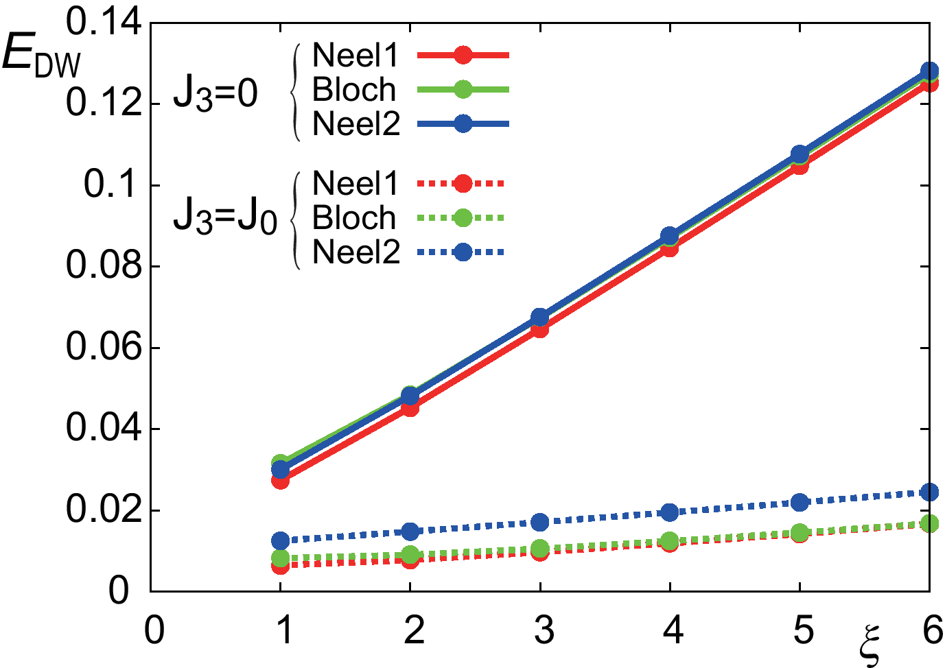
The domain wall width should be optimized as a variational parameter in Eq. (10). It is found that the energy is decreased as is decreased down to . See Supplementary Information .1. Therefore, the width of the domain wall is typically the lattice constant in this model. The reason is basically that the kinetic energy in the 2D effective Hamiltonian is solely given by the SOI and hence there is no length scale due to the SOI other than the lattice constant. The detailed discussion is given in Supplementary Information .2. However, as mentioned above, the lattice constant of the present tight-binding Hamiltonian is that of the coarse grained model, and hence the distinction between Neel and Bloch walls still makes sense. Also the width depends on the additional single-ion magnetic anisotropy term which exists in the real material but not included in the present model. We have numerically confirmed that the qualitative features of the results do not depend on , and hence we have shown the results for for illustrative purpose in order to clearly show the difference between the Neel and Bloch walls. See .1 in Supplementary Information.
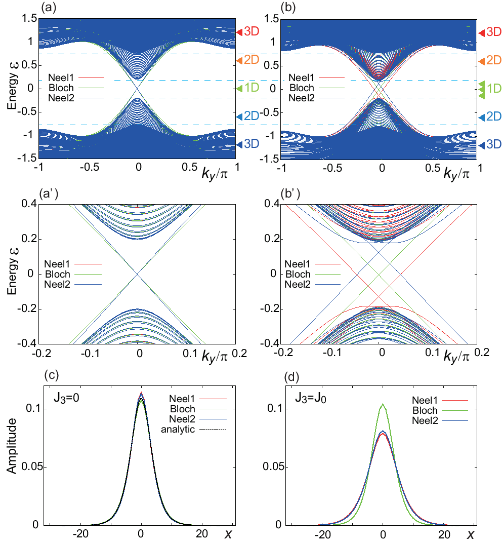
Edge modes. A magnetic domain wall separates the two domains with up and down spins, i.e., the regions of . Therefore, the difference of is and hence one chiral edge channel is expected to appear along the domain wall. We show the energy dispersion and the probability distribution of the edge channel wave function along the direction obtained numerically for in Figs. 2(a) and (a’), and in Figs.2(b) and (b’), respectively.
There are three energy scales in the band structure as shown in Figs. 2(a) and (b). One is the 3D bulk band structure which exists for . The second is the 2D surface band structure which exists for . The last is the 1D edge states along the domain wall which exists for .
When , the dispersion and wave function of the edge modes are almost independent of as shown in Figs. 2(a) and (a’). This is consistent with Eq. (6) with . Since the coupling is Ising-like, there is no dependence for the surface states. We have determined numerically the probability distribution of the wave function at , which we show in Figs. 2(c) and (d).
We present a clear physical picture for the zero-energy edge mode for . The wave function is analytically given by the Jackiw–Rebbi solution JR ,
| (12) |
with a normalization constant . It can be obtained by solving the differential equation given from Eq. (6)
| (13) |
Indeed, it well explains the numerical data in Fig. 2(c). The half width of the wave function is the same order of the domain wall width .
On the other hand, the edge modes depend on when as shown in Figs. 2(b) and (b’). This is again consistent with Eq. (6) with . The energy dispersion of the edge mode is well described by
| (14) |
as we derive by the first-order perturbation in Supplementary Information .3. Note that the spatial extent of the wave function is affected by the energy separation between the in-gap state and the edge of the bulk density states, and hence depends on in this case.
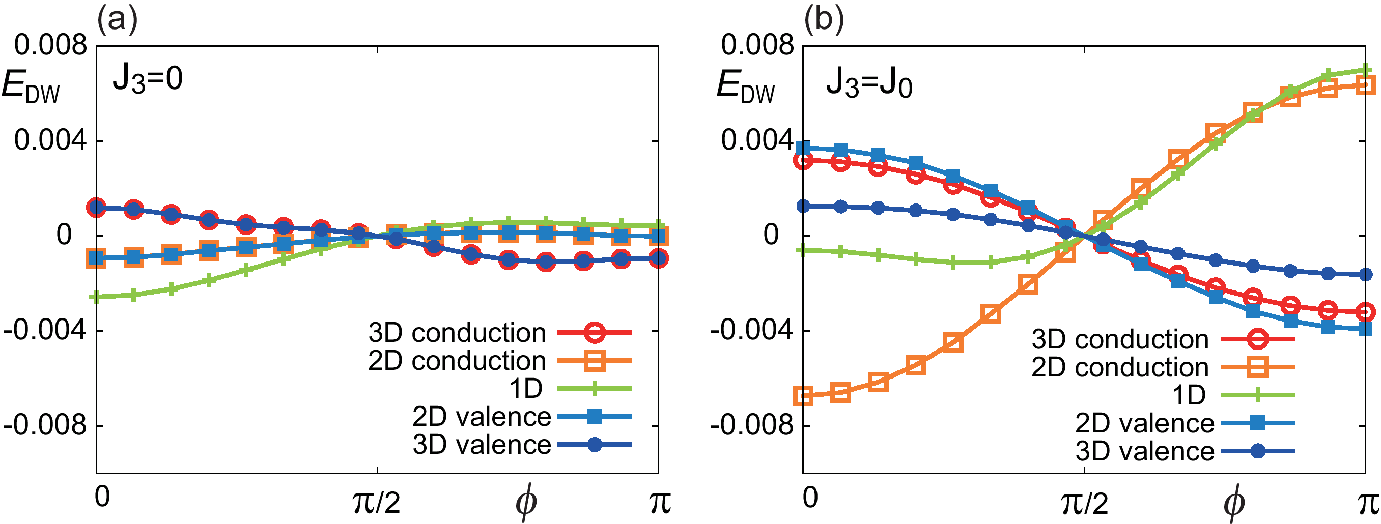
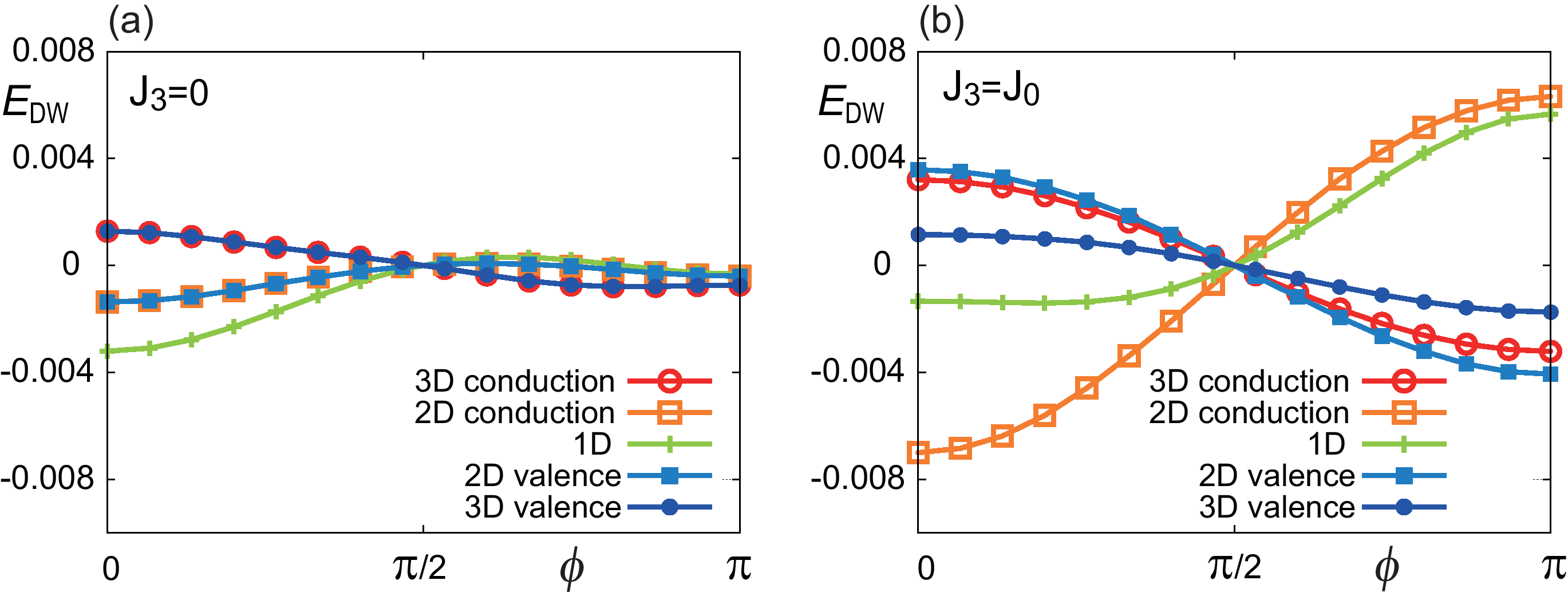
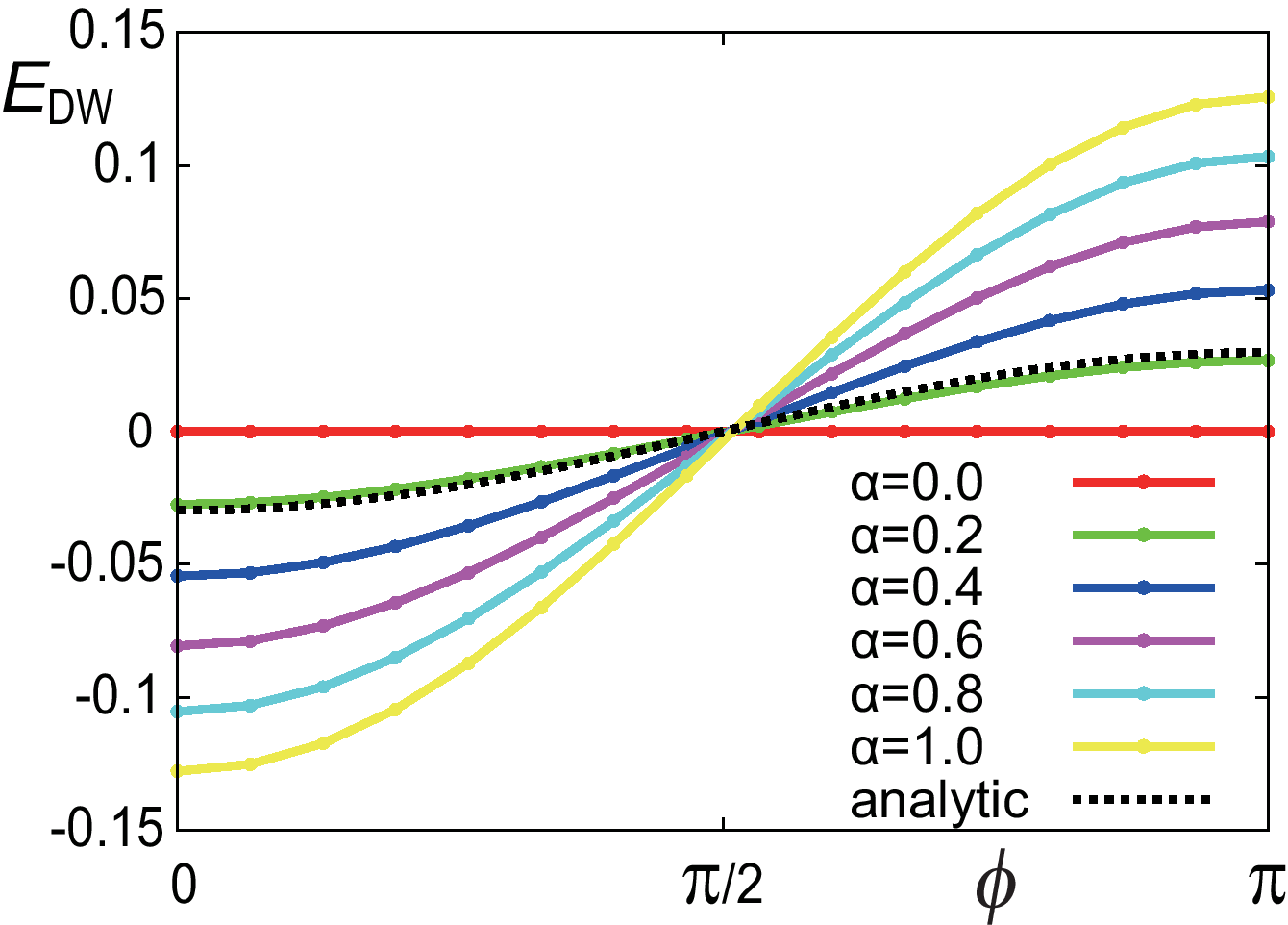
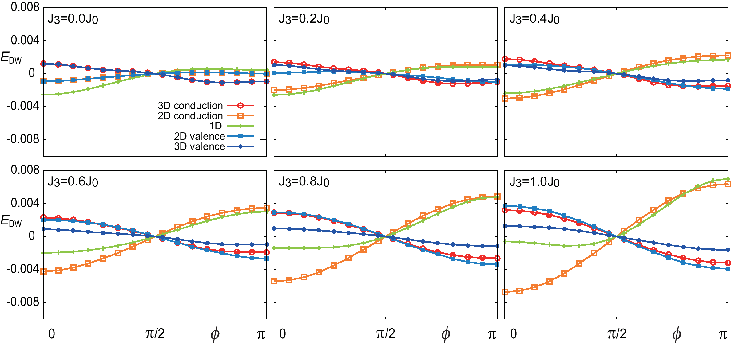
Domain wall energy. We show in Fig. 3 the -dependence of the domain wall energy measured from the value at (Bloch wall) for several values of the chemical potential when the magnetic layer is at the top surface. (The absolute value of the domain wall energy compared with the uniform magnetization is a more subtle quantity, which depends also on the magnetic anisotropy term , and therefore we do not address it in this paper.) The domain wall energy is the same for and due to the mirror symmetry with respect to plane as , . Therefore, it is enough to show the results for . behaves quite differently between the cases of and . (In Supplementary Information .4, Fig. 9 illustrates for various values of .) When , the Neel wall with is the most stable for the chemical potential in the 2D valence/conduction bands or inside the gap. When is in the 3D bands, the Neel wall with becomes the most stable. In this case, the system possesses the particle–hole symmetry as shown in Supplementary Information .5. As a result, the energy is symmetric between , which is also verified by our numerical calculations.
On the other hand, when , the particle–hole symmetry is lost. For in Fig. 3(b), the minimum energy configuration changes from (Neel 2) for large positive (in the 3D conduction band), turns to (Neel1) for in the 2D conduction band, approaches to (Bloch) for within the gap, and eventually to (Neel 2) for . This means that one can control the angle of the domain wall by the gate voltage, which changes the chemical potential. This is one of our main results in the present paper. This change of the stable magnetic structure is understood analytically in terms of the effective Dzyaloshinskii–Moriya (DM) interaction induced from the TI surface state as discussed below.
When the chemical potential is in the 2D surface band , the stability of a magnetic domain wall can be understood in terms of the effective surface DM interaction due to the Weyl surface states. In order to derive the effective Hamiltonian for the magnets, we integrate out the fermion degrees of freedom, namely, calculate the following effective action
| (15) |
where , , and is the spin susceptibility,
| (16) |
and is the Green’s function for the Weyl Hamiltonian (6) without the exchange terms. We obtain
| (17) |
with
| (18) |
The detailed derivation is shown in Supplementary Information .2. It is zero within the band gap of the 2D surface state. The sign of the DM interaction is positive for and negative for . Namely, we can control the sign of the DM interaction by changing the chemical potential by the gate voltage. It is noted that the sign change of the DM interaction stems from the helicity difference of the momentum–spin locking on the conduction and valence bands. We evaluate the domain wall energy change due to the DM interaction. Substituting the domain wall texture (10) into Eq. (17), we obtain
| (19) |
with the length of the domain wall . It takes the minimum energy for the Neel domain wall with () for ().
Finally, we briefly note the general case . When increases from zero, the exchange interaction on the surface changes from the Ising-like anisotropic form to the Heisenberg-like isotropic form. Therefore, the energy difference among the various domain walls continuously increases. The numerical results are shown in Supplementary Information .4.
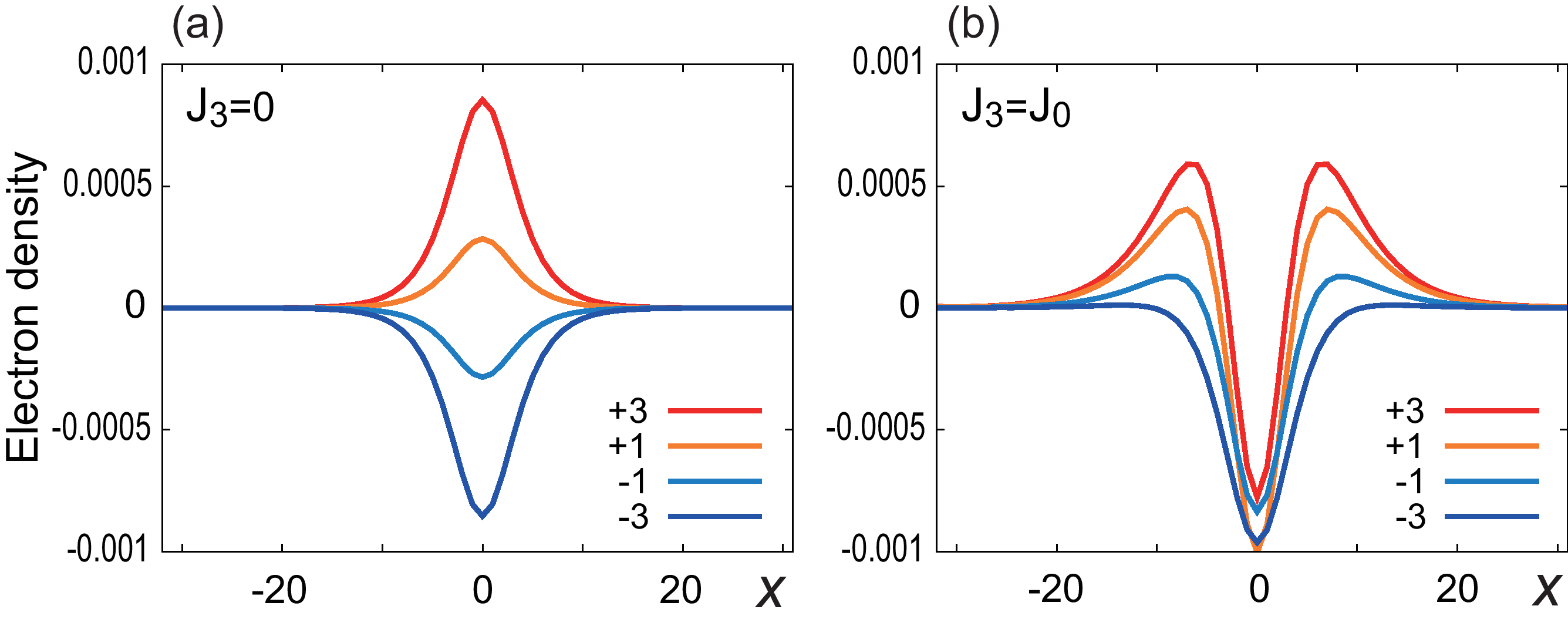
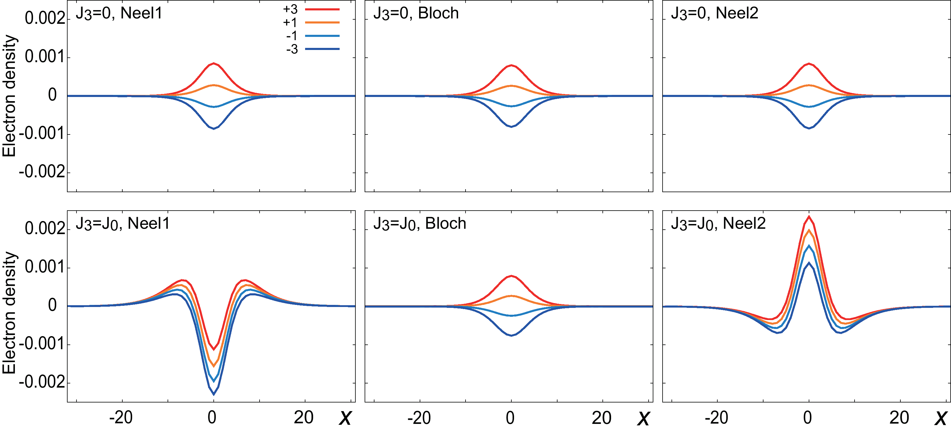
Electron density distribution. We demonstrate in Fig. 4 the electron density distribution of the upper half layers for the minimum-energy domain wall configuration numerically calculated via the expression
| (20) |
where are the eigenfunctions of the 3D Hamiltonian with the band index . (For the electron density distributions corresponding to general domain wall configurations, see Supplementary Information .6.) When (Fig. 4(a)), the density distribution is uniform for , while it is localized at the domain wall for inside the bulk band gap. The density distribution is inverted between .
We may explain the electron accumulation analytically as follows. For the edge state is well described by the Jackiw–Rebbi mode Eq. (12). It gives the edge channel wave function at zero energy for electrons or holes. When the chemical potential is shifted, the electrons or holes accumulate into the edge states for within the 2D surface band gap. Hence, by considering the density of states for the edge channel, the electron density is given by
| (21) |
On the other hand, when , there are two peaks in the density distribution of the Neel domain wall as found in Fig. 4(b). To understand this behavior, we recall that the electron accumulation due to the spin texture has previously been shown to be Nomura2
| (22) |
for a smooth magnetic texture which remains almost constant for all over the sample. Following Ref. Nomura2 , this relation can be derived by considering the Chern–Simons action
| (23) |
and the gauge field is
| (24) |
By using the relation , Eq. (22) is be obtained.
The total accumulation must consist of the zero-energy edge contribution and the background contribution , . The Neel-type magnetic configurations contributes to the electron accumulation , but that there is no such an accumulation in the Bloch-type magnetic configurations because . Thus, may be the difference of the electron accumulation between the Neel and Bloch domain walls. In our case, for the Neel wall is
| (25) |
with the use of sech in Eq. (22) for a Neel domain wall.
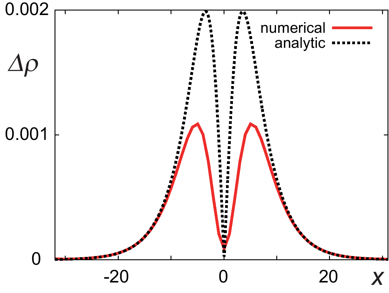
To confirm this scenario, we plot the difference in the charge density between the Neel and Bloch walls with the equal chemical potential in Fig. 5. The formula Eq. (25) captures the key structure of the numerical data as in Fig. 5. Therefore, the peculiar double peak structure in Fig. 4(b) stems from the combination of the chiral edge channel and the spatial variation of the spin texture. The amplitude can be enhanced or reduced, depending on the domain wall type and the filling of the edge channel.
Finally, we note that we can estimate the charging energy with the obtained electron distributions, and conclude that the charging energy is negligible compared with the band energy. The detailed discussion is shown in Supplementary Information .7.
Discussions
The origin of the ferromagnetism in doped TI is an important issue. A first-principles calculation on Mn-doped Bi2Te3 Henk indicates that the Hamiltonian Eq. (2) is a good effective model for the surface states. The gap depends strongly on the direction of the magnetization ; it is meV when is perpendicular to the surface, while the shift in the in-plane momentum occurs when is parallel to the surface. From the comparison between the gap in the former case and the energy shift at in the latter case, it is concluded that in Eq. (2), i.e., . Physically, the Cr and Mn atoms are replacing Bi, and probably the coupling to the neighboring Te -orbitals are stronger than to those of Bi atoms, which results in this orbital dependent exchange interaction. Experimentally, the gating can tune the chemical potential and it has been argued from the dependence of ferromagnetic on that the coupling to the surface Weyl fermions is the origin of the ferromagnetism Joe2 . Therefore, the model Eq. (2) is appropriate also from this viewpoint.
However, in real materials, the magnetic ions are not selectively doped on the surface but are distributed in the whole sample. Therefore, it is expected that the magnetization behaves uniformly along the direction (perpendicular to the surface) for the thin film samples with the thickness of the order of 8 nm Joe . The bulk mechanism of ferromagnetism in doped TI is studied theoretically also Yu ; Kurebayashi . In Supplementary Information .8, we study the dependence on the depth of the magnetic layer. When the magnetization on the top and bottom surfaces are the same, the energies of domain wall (Neel 1) and domain wall (Neel 2) are degenerate because of the mirror symmetry with respect to the plane separating the upper and lower halves of the film. This argument, however, assumes the equivalence between the top and bottom surfaces, which is not satisfied in general experimental setups. Actually, it is observed that the Weyl points on top and bottom surfaces are different in energy typically of the order of 50meV Yoshimi , and this symmetry is broken. Therefore, we expect that the type of the domain wall can be manipulated by gating.
As for the existence of the domain walls, they are naturally introduced in the hysteresis loop in the magnetic field - magnetization curves. Actually the longitudinal resistance is found to have the peak at the ends of the hysteresis loop, which is likely due to the chiral edge channel associated with the domain wall Joe . An interesting possibility is the formation of skyrmions, which corresponds to the circular closed loop of a domain wall. It is well known the charge doping into quantum Hall ferromagnet results in the formation of skyrmions QHE . It remains an open issue if the skyrmions can appear in the quantized anomalous Hall system on 3D TI.
Methods
We have used the 3D Hamiltonian Eq. (4) for the numerical calculations. We assume the periodic boundary condition for the and directions, and the open boundary condition for the direction. We put non-uniform magnetic moments for the direction. Therefore, is a good quantum number. By summing up eigenenergies and amplitudes of eigenfunctions below a certain particle number, we obtain the total energy and the electron density distribution. We set the zero of the energy for that of the Bloch wall, and the zero of the density for that of the half-filling case. In Fig. 5(c), we compared the density of a Neel wall and a Bloch wall with the same chemical potential. We set for the main text.
Acknowledgements
The authors are grateful for insightful discussions with M. Kawasaki and Y. Tokura. R. W. and M. E. are grateful for helpful conversations with R. Takahashi and H. Isobe. R. W. was supported by Grant-in-Aid for JSPS Fellows. This work was supported by Grant-in-Aids for Scientific Research (Nos. 24224009, 25400317, and 15H05853) from the Ministry of Education, Culture, Sports, Science and Technology (MEXT) of Japan.
Author Contributions
R. W. performed the numerical calculations. R.W., M. E., and N. N. contribute in analyzing the data and writing the paper.
Competing Financial Interests
The authors declare that they have no competing financial interests.
References
- (1) Hasan, M. Z. & Kane, C. L. Colloquium: Topological insulators. Rev. Mod. Phys. 82, 3045–3067 (2010).
- (2) Qi, X.-L. & Zhang, S.-C. Topological insulators and superconductors. Rev. Mod. Phys. 83, 1057–1110 (2011).
- (3) He, H. T. et al. Impurity effect on weak antilocalization in the topological insulator Bi2Te3. Phys. Rev. Lett. 106, 166805 (2011).
- (4) Haldane, F. D. M. Model for a quantum Hall effect without Landau levels: Condensed-matter realization of the “parity anomaly”. Phys. Rev. Lett. 61, 2015–2018 (1988).
- (5) Onoda, M & Nagaosa, N. Quantized anomalous Hall effect in two-dimensional ferromagnets: Quantum Hall effect in metals. Phys. Rev. Lett. 90, 206601 (2003).
- (6) Yu, R. et al. Quantized anomalous Hall effect in magnetic topological insulators. Science 329, 61–64 (2010).
- (7) Nomura, K. & Nagaosa, N. Surface-quantized anomalous Hall current and the magnetoelectric effect in magnetically disordered topological insulators. Phys. Rev. Lett. 106, 166802 (2011).
- (8) Abanin, D. A. & Pesin, D. A. Ordering of magnetic impurities and tunable electronic properties of topological insulators. Phys. Rev. Lett. 106, 136802 (2011).
- (9) Garate, I. & Franz, M. Inverse spin-galvanic effect in the interface between a topological insulator and a ferromagnet. Phys. Rev. Lett. 104, 146802 (2010).
- (10) Yokoyama, T., Zang, J. & Nagaosa, N. Theoretical study of the dynamics of magnetization on the topological surface. Phys. Rev. B 81, 241410(R) (2010).
- (11) Tserkovnyak, Y. & Loss, D. Thin-film magnetization dynamics on the surface of a topological insulator. Phys. Rev. Lett. 108, 187201 (2012).
- (12) Linder, J. Improved domain-wall dynamics and magnonic torques using topological insulators. Phys. Rev. B 90, 041412(R) (2014).
- (13) Ferreiros, Y. & Cortijo, A. Domain wall motion in junctions of thin-film magnets and topological insulators. Phys. Rev. B 89, 024413 (2014).
- (14) Baum, Y. & Stern, A. Density-waves instability and a skyrmion lattice on the surface of strong topological insulators. Phys. Rev. B 86, 195116 (2012).
- (15) Mendler, B., Kotetes, P. & Sch’́on, G. Magnetic order on a topological insulator surface with warping and proximity-induced superconductivity. Phys. Rev. B 91, 155405 (2015).
- (16) Hurst, H. M., Efimkin, D. K., Zang, J. & Galitski, V. Charged skyrmions on the surface of a topological insulator. Phys. Rev. B 91, 060401(R) (2015).
- (17) Chen, Y. L. et al. Massive dirac fermion on the surface of a magnetically doped topological insulator. Science 329, 659–662 (2010).
- (18) Zhang, J. et al. Topology-driven magnetic quantum phase transition in topological insulators. Science 339, 1582–1586 (2013).
- (19) Chang, C.-Z. et al. Experimental observation of the quantum anomalous Hall effect in a magnetic topological insulator. Science 340, 167–170 (2013).
- (20) Checkelsky, J. G. et al. Trajectory of the anomalous Hall effect towards the quantized state in a ferromagnetic topological insulator. Nat. Phys. 10, 731–736 (2014).
- (21) Chang, C.-Z. et al. High-precision realization of robust quantum anomalous Hall state in a hard ferromagnetic topological insulator. Nat. Mater. 14, 473–477 (2015).
- (22) Bestwick, A. J., Fox, E. J., Kou, X., Pan, L. & Wang, K. L. Precise quantization of the anomalous Hall effect near zero magnetic field. Phys. Rev. Lett. 114, 187201 (2015).
- (23) Kou, X. et al. Scale-invariant quatnum anomalous Hall effect in magnetic topological insulators beyond the two-dimensional limit. Phys. Rev. Lett. 113, 137201 (2014).
- (24) Figueroa, A. I. et al. Magnetic Cr doping of Bi2Se3: Evidence for divalent Cr from x-ray spectroscopy. Phys. Rev. B 90, 134402 (2014).
- (25) Ni, Y., Zhang, Z., Nlebedim, I. C., Hadimani, M. R. & Tuttle, G. L. Ferromagnetism of magnetically doped topological insulators in CrxBi2-xTe3 thin films. J. Appl. Phys. 117, 17C748 (2015).
- (26) Parkin, S. S. P., Hayashi, M. & Thomas, L. Magnetic domain-wall racetrack memory. Science 320, 190–194 (2008).
- (27) Ryu, K.-S., Thomas, L., Yang, S.-H. & Parkin, S. Chiral spin torque at magnetic domain walls. Nat. Nanotech. 8, 527–533 (2013).
- (28) Rojas Sánchez, J. C. et al. Spin-to-charge conversion using Rashba coupling at the interface between non-magnetic materials. Nat. Commun. 4, 2944 (2013).
- (29) Zhang, H., Liu, C.-X., Qi, X.-L., Dai, X., Fang, Z. & Zhang, S.-C. Topological insulators in Bi2Se3, Bi2Te3 and Sb2Te3 with a single Dirac cone on the surface. Nat. Phys. 5, 438–442 (2009).
- (30) Liu, C.-X. et al. Model Hamiltonian for topological insulators. Phys. Rev. B 82, 045122 (2010).
- (31) Shan, W.-Y., Lu, H.-Z. & Shen, S.-Q. Effective continuous model for surface states and thin films of three-dimensional topological insulators. New J. Phys. 12, 043048 (2010).
- (32) Henk, J. et al. Topological character and magnetism of the Dirac state in Mn-doped Bi2Te3. Phys. Rev. Lett. 109, 076801 (2012).
- (33) Jackiw, R. & Rebbi, C. Solitons with fermion number 1/2. Phys. Rev. D 13, 3398–3409 (1976).
- (34) Nomura, K. & Nagaosa, N. Electric charging of magnetic textures on the surface of a topological insulator. Phys. Rev. B 82, 161401(R) (2010).
- (35) Checkelsky, J. G., Ye, J., Onose, Y., Iwasa, Y. & Tokura, Y. Dirac-fermion-mediated ferromagnetism in a topological insulator. Nat. Phys. 8, 729–733 (2012).
- (36) Kurebayashi, D. & Nomura, K. Weyl semimetal phase in solid-solution narrow-gap semiconductors. J. Phys. Soc. Jpn. 83, 063709 (2014).
- (37) Yoshimi, R. et al. Quantum Hall effect on top and bottom surface states of topological insulator (Bi1-xSbx)2Te3 films. Nat. Commun. 6, 6627 (2015).
- (38) Perspectives in Quantum Hall Effects, edited by Das Sarma, S. & Pinczuk, A. (Wiley, New York, 1997).
Supplementary Information for
“Domain wall of a ferromagnet on a three-dimensional topological insulator”
.1 Width dependence of the domain wall energy
Figure 6 shows the domain wall energy with the width as a function of for ((a)) and ((b)). The qualitative behavior is the same as that of Fig. 3 for in the main text. Figure 7 shows as a function of . It is seen that the smaller is preferred for all the cases. For the illustrative purpose, we set in the main text so that we can capture the difference between various domain wall structures.
.2 Effective action
We derive an effective action of the 2D Weyl Hamiltonian. The effective action is obtained by calculating the susceptibility in the one-loop approximation,
| (26) |
where and . For the region , one can expand with respect to , while for the region , the mass can be put to be zero for the derivation.
We derive the DM interaction and the exchange interaction by calculating the
non-diagonal element of in the massive Weyl Hamiltonian.
We estimate the domain wall width by calculating the diagonal element of
in the massless Weyl Hamiltonian.
The DM and exchange interaction:
Firstly, we derive the DM interaction and the exchange interaction from the massive Weyl Hamiltonian. The continuum theory of the 2D Hamiltonian is described by
| (27) |
The Green’s function reads
| (28) |
With the use of the Green’s function, the susceptibility is given by
| (29) |
We put , and take the limit. We can show
| (30) |
with
| (31) |
The susceptibility is inverted between . The DM interaction reads
| (32) |
with . This is Eq. (18) in the main text.
We calculate the diagonal terms up to ,
| (33) |
with
| (34) |
They contain the ultra-violet momentum cut-off , which is naturally given by the 3D band or the lattice constant. The -independent terms yield
| (35) |
which describes the easy-axis anisotropy, while the -dependent terms yield
| (36) |
which acts as the exchange interaction.
The domain wall width:
Next, we derive the effective action for . We make the following decomposition of Eq. (29),
| (37) |
We calculate the term,
| (38) |
and so on. The results for Eq. (37) read up to as
| (39) | ||||
| (40) |
The domain wall width is estimated as follows. First, assume that is much smaller than , and use the expansion Eqs. (S15) and (S17). Then, we demand the anisotropy energy, i.e., the difference between and , is equal to the elastic energy. However, the obtained is much larger than since . Therefore, we need to look for in the region , i.e., using Eq. (S21). This results in
| (41) |
which satisfies and hence gives the self-consistent estimation.
.3 Edge channel along the domain wall
We investigate the edge channel along the domain wall,
| (42) |
The exact solution is obtained when , which is known as the Jackiw-Rebbi solution. The continuum theory of the 2D Hamiltonian in Eq. (2) is described by
| (43) |
The eigenequation for is
| (44) |
The solution which is localized around the domain wall is
| (45) |
which is Eq. (12) in the main text, with the normalization constant
| (46) |
In the presence of and terms for small , we may estimate the energy as
| (47) |
which is in Eq. (14) in the main text.
Figure 8 shows numerical results on the shift of energy at as a function of . They are well fitted by the cosine curve obtained by the first-order perturbation Eq. (47) for .
.4 dependence of the domain wall energy
.5 Symmetry Analysis
Here, we summarize the symmetry properties of the models presented in the main text.
3D Hamiltonian:
The 3D tight-binding Hamiltonian in Eq. (4) is given by
| (48) |
where is the chemical potential. Its complex conjugate is
| (49) |
We consider an operator
| (50) |
which transforms the Hamiltonian as
| (51) |
On the other hand, the particle-hole operator
| (52) |
transforms the Hamiltonian as
| (53) |
This operator is the generator of the particle-hole transformation together with , and . The energy spectrum is symmetric (asymmetric) between the positive and the negative energy when ().
The time-reversal operator is given by
| (54) |
which transforms the Hamiltonian as
| (55) |
The chiral symmetry is defined by the product of the particle-hole symmetry and the time-reversal symmetry,
| (56) |
which transforms the Hamiltonian as
| (57) |
The chiral transformation is preserved when , and .
We make the mirror symmetry along direction
| (58) |
The domain wall energy is the same for and due to the
mirror symmetry along the direction as ,
. Therefore it is enough to show the results for
.
2D Hamiltonian:
The 2D Hamiltonian for the surface state is given by
| (59) |
Its complex conjugate is
| (60) |
The time-reversal operator is given by
| (61) |
which transforms the Hamiltonian as
| (62) |
When , the time-reversal transformation symmetry is preserved,
| (63) |
On the other hand, when , there is a symmetry
| (64) |
with the time-reversal symmetry operator even when .
.6 Electron accumulation for the Neel wall and the Bloch wall
Figure 10 shows the electron density distribution for the cases of Neel and Bloch walls. There are two peak structures for for the Neel domain wall, which come from term in Eq. (22) in the main text.
.7 Charging energy
We evaluate the charging energy for three cases: (i) heavily doped case where the Fermi energy is in the 2D conduction band, (ii) half-filling case, and (iii) the case where the Fermi energy is deviated from the half-filling but in the 2D bang gap, and show that the charging energy can be neglected compared with the band energy.
We take the lattice constant Å as the unit. Then, the unit of the Coulomb energy is
| (65) |
where, we have used for the TIs.
(i) Heavily doped case. For the heavily doped case, we can neglect the long-range Coulomb interaction and consider only the onsite repulsion because of the screening. According to numerical calculations, the electron distribution amplitudes is less than , and the width is about . Therefore, the charging energy is
| (66) |
where we have taken into account the two domain walls due to the periodic boundary condition. On the other hand, the order of the band energy is
| (67) |
where we have used for the TIs. is about ten times larger than . Therefore, we can neglect the effect of the charging energy.
(ii) Half-filling case. We have to consider the long-range Coulomb interaction.
| (68) | ||||
| (69) | ||||
| (70) | ||||
| (71) | ||||
| (72) |
On the other hand, the band energy is calculated as
| (73) |
where we have used the density of states for the Weyl Hamiltonian. Therefore, is proportional to as in the Fig. 7. If we use the parameter used in the calculation, we get . In the Fig. 7, we obtain for the Ising case and for the Heisenberg case. In the evaluation, we use the numerical result.
We obtain the optimized by minimizing .
| (74) |
For the half-filling case, only the term contributes the charging, and the amplitude is less than , and . Therefore, we get the optimized as
| (75) |
for the Heisenberg case. Therefore, we conclude that the effect of the charging energy is negligible for the half-filling case.
(iii) The case where the Fermi energy is in the 2D gap. In this case, the Jackiw–Rebbi solutions accumulate. We can estimate for the electron doped system. On the other hand, the particle number is expressed as the function of the Fermi energy.
| (76) |
Therefore,
| (77) |
The Fermi energy which gives is eV. It is much larger than the surface gap ( meV). Therefore, the charging energy is negligible for the arbitrary Fermi energy.
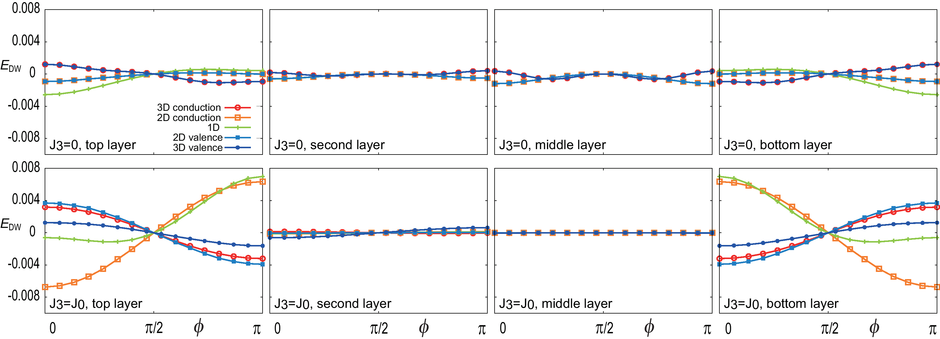
.8 Layer dependence of the domain wall energy
Figure 11 shows the domain wall energy for various depths of the magnetic layer. In the case of the second and middle layers, the energy differences are small because the amplitudes of surface states are small. The domain wall energy for the top layer with is identical to that of the bottom layer with , while the domain wall energy of the middle layer is symmetric between and , because of the mirror symmetry at the middle layer.