An error-resilient non-volatile magneto-elastic universal logic gate with ultralow energy-delay product
A long-standing goal of computer technology is to process and store digital information with the same device in order to implement new architectures. One way to accomplish this is to use nanomagnetic ‘non-volatile’ logic gates that can perform Boolean operations and then store the output data in the magnetization states of nanomagnets, thereby doubling as both logic and memory. Unfortunately, many proposed nanomagnetic gates do not possess the seven essential characteristics of a Boolean logic gate : concatenability, non-linearity, isolation between input and output, gain, universal logic implementation, scalability and error resilience. More importantly, their energy-delay products and error-rates vastly exceed that of conventional transistor-based logic gates, which is a drawback. Here, we propose a non-volatile voltage-controlled nanomagnetic logic gate that possesses all the necessary characteristics of a logic gate and whose energy-delay product is 2 orders of magnitude less than that of other nanomagnetic (non-volatile) logic gates and 1 order of magnitude less than that of (volatile) CMOS-based logic gates. The error-resilience is also superior to that of other known nanomagnetic gates.
There is significant interest in ‘non-volatile logic’ because the ability to store and process information with the same device affords immense flexibility in designing computing architectures. Non-volatile logic based architectures can reduce overall energy dissipation by eliminating refresh clock cycles, improve system reliability and produce ‘instant-on’ computers with virtually no boot delay. A number of non-volatile universal logic gates have been proposed to date cowburn ; ney ; behin-aein , but they do not necessarily satisfy all the requirements for a logic gate behin-aein2 ; Waser and therefore may not be usable in all circumstances. Ref. [cowburn, ] proposed an idea where digital bits are stored in the magnetization orientations of an array of dipole-coupled nanomagnets and dipole coupling between neighbors elicits logic operation on the bits. This gate is not concatenable since the input and output bits are encoded in dissimilar physical quantities: the inputs are encoded in directions of magnetic fields and the output is encoded in the magnetization orientation of a nanomagnet. Thus, the output of a preceding gate cannot act as the input to the succeeding gate without additional transducer hardware to convert the magnetization orientation of a nanomagnet into the direction of a magnetic field. The gate also lacks true gain since the energy needed to switch the output comes from the inputs and not an independent source such as a power supply. Additionally, the strength of dipole coupling between magnets decreases as the square of the magnet’s volume, which limits scalability. Finally, dipole coupling is not sufficiently resilient against thermal noise, resulting in unacceptably large dynamic bit error rate in dipole-coupled logic gates roychowdhury ; salehi ; bokor .
Ref. [ney, ] proposed a different construct where a NAND gate was implemented with a single magneto-tunneling junction (MTJ) placed close to four current lines, two of which are input lines, the third is required for an initialization operation, and the fourth is the output line. The input bits are coded in the directions of the currents in the two input lines, while the output bit is coded in the magnitude of the current in the output line. The input currents generate a magnetic field (whose direction is determined by the directions of the input currents) which then orients the magnetization of the MTJ’s soft layer in the direction of the field and determines the MTJ resistance as well as the magnitude of the output current. The magnitude of the output current was shown to be a NAND function of the directions of the input currents ney . Slightly different renditions of this idea have been proposed lee and an experimental demonstration of MTJ-based logic has been reported jpwang . Unfortunately, this gate too is not directly concatenable since the input bits are encoded in the directions of the input currents while the output bit is encoded in the magnitude of the output current. Moreover, since it is difficult to confine magnetic fields to small regions, the separation between neighboring devices must be large. Individual devices can be small in size, but because the inter-device pitch is large, the device density will be small. There is also some chance that the output current can, by itself, switch the magnetization of the soft magnetic layer and therefore affect its own state. This is equivalent to lack of isolation between the input and the output, which makes gate operation unreliable. Finally, another MTJ-based logic gate has been proposed recently kuntal_new , but it requires a feedback circuit to operate (which makes it energy-inefficient and error-prone) and even the logic functionality is questionable comment . Thus, while these devices are interesting in their own right, they may not be universally usable.
A more recent scheme that overcomes most of the above shortcomings was proposed in Refs. [behin-aein, ] and [behin-aein2, ]. It implements non-volatile logic with magnets switched by spin currents. Both computation and communication between gates are carried out with a sequence of clock pulses. Unfortunately, its error-resilience has not been examined. Normally, magnetic devices are much more error-prone than transistors since magnetization dynamics is easily disrupted by thermal noise roychowdhury ; salehi . Logic has stringent requirements on error rates and it is imperative to evaluate the dynamic bit error probability of any gate to assess its viability.
Finally, the most important metric for a logic gate is the energy-delay cost. All non-volatile magnetic logic schemes are deficient in this area. The scheme in Ref. [ney, ] uses current-generated magnetic fields to switch magnets and hence would dissipate at least 109 kT of energy per gate operation at room temperature to switch in 1 ns salehi2 (energy-delay product = 410-21 J-s). A recent experiment conducted to demonstrate switching of nanomagnets with on-chip current-generated magnetic fields ended up dissipating approximately 1012 kT of energy per switching event, despite switching in 1 s (energy-delay product = 410-15 J-s) nd . The scheme in Ref. [behin-aein, ] is expected to dissipate between 105 and 106 kT of energy when it switches in 1 ns (energy-delay product = 410-25 - 410-24 J-s) sharad , although a lower energy-delay product may be possible with design optimization sarkar . On the other hand, a low-power CMOS transistor is claimed to dissipate only 103 kT of energy when it switches in 0.1 ns (energy-delay product = 310-28 J-s) nikonov , although more realistic estimates based on available data predict energy dissipation of 450 aJ to switch in 0.34 ns (energy-delay product = 1.510-25 J-sec) Datta-review . Since any non-mainstream technology must eclipse mainstream CMOS technology by at least close to an order of magnitude to be worthy of consideration, the magnetic logic ideas have languished despite their coveted non-volatility.
In this report, we propose a non-volatile nanomagnetic NAND gate that is switched with voltage (not current) unlike the other schemes. It has an energy-delay product 2.7810-26 J-s which is smaller than that of other magnetic logic schemes by almost two orders of magnitude and that of CMOS by almost one order of magnitude. The energy-delay product however, by itself, is not the most meaningful metric for benchmarking device performance. It is always possible to reduce this product arbitrarily by sacrificing reliability. For example, one can forcibly switch a device faster and also dissipate less energy to switch (which will reduce the energy-delay product), but at the cost of increased switching failures. A more meaningful metric may be the product of energy, delay and failure (error) probability. The error probability for the proposed NAND gate has been evaluated rigorously from stochastic simulations. With careful choice of parameters, it is possible to reduce the error probability to below 10-8 at room temperature, which is remarkable for magnetic logic (magnetic logic is typically much more error-prone than transistor logic). Finally, the proposed gate fulfills all the requirements for logic. Therefore, it is possibly the first nanomagnetic logic gate that has the cherished advantage of magnetic logic gates (non-volatility) and yet none of the usual disadvantages.
The proposed gate structure is shown in Fig. 1(a). It is implemented with a skewed MTJ stack, passive resistors and , a bias dc voltage , and a constant current source . The current source is not used to switch the gate, but merely to produce an output voltage representing the output logic bit. Input bits are encoded in input voltages . Both input and output bits are encoded in the same physical quantity, voltage, which allows direct concatenation.
The bottom layer of the MTJ stack is an elliptical magnetostrictive (metallic) nanomagnet (Terfenol-D) and the top layer is a non-magnetostrictive elliptical (metallic) synthetic anti-ferromagnet (SAF) with large shape anisotropy. The top layer acts as the hard (or pinned) layer and the bottom layer acts as the soft (or free) layer of the MTJ. There is a small permanent magnetic field directed along the minor axis of the magnetostrictive nanomagnet (+y-direction) which brings its two stable magnetization orientations out of the ellipse’s major axis and aligns them along two mutually perpendicular in-plane directions that lie between the major and minor axes (Fig. 1(b)) tiercelin ; Giordano . The major axis of the top SAF layer is aligned collinear with one of the two stable magnetization orientations of the soft magnet. It is then permanently magnetized in the direction anti-parallel to that stable orientation. As a result, when the magnetization of the soft layer is in this stable orientation, the hard and soft layers have anti-parallel magnetization resulting in high MTJ resistance. When the soft layer’s magnetization is in the other stable direction, the MTJ resistance is lowered.
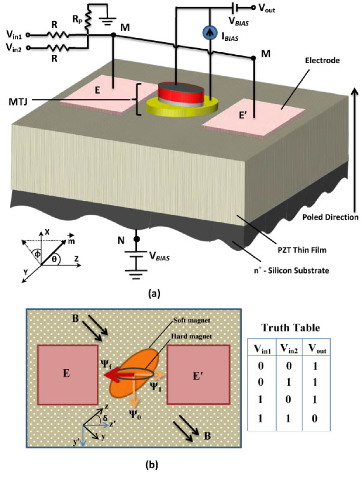
Two electrodes and are delineated on the PZT surface such that the line joining their centers is collinear with the major axis of the hard layer and hence also the first stable orientation of the soft layer. The electrode lateral dimensions, the separation between their edges, and the PZT film thickness are all approximately equal. These two electrodes are electrically shorted. Whenever an electrostatic potential difference appears between them and the underlying silicon substrate (between point- and point- in Fig. 1(a)), the PZT layer is strained. Since the electrode in-plane dimensions are comparable to the PZT film thickness, the out-of-plane () expansion/contraction and the in-plane () contraction/expansion of the piezoelectric regions underneath the electrodes produce a highly localized strain field under the electrodes Lynch2013 . Furthermore, since the electrodes are separated by a distance approximately equal to the PZT film thickness, the interaction between the local strain fields below the electrodes will lead to a biaxial strain in the PZT layer underneath the soft magnet Lynch2013 . This biaxial strain (compression/tension along the line joining the electrodes and tension/compression along the perpendicular axis) is transferred to the soft magnetostrictive magnet in elastic contact with the PZT, thus rotating its magnetization via the Villari effect. This happens despite any substrate clamping and despite the fact that the electric field in the PZT layer just below the magnet is approximately zero Lynch2013 . Some of the generated strain may even reach the top hard magnet li , but since the hard magnet is very anisotropic in shape and is not magnetostrictive, its magnetization will not rotate perceptibly. Rotation of the magnetization of the soft layer of an MTJ due to strain has been recently demonstrated experimentally li .
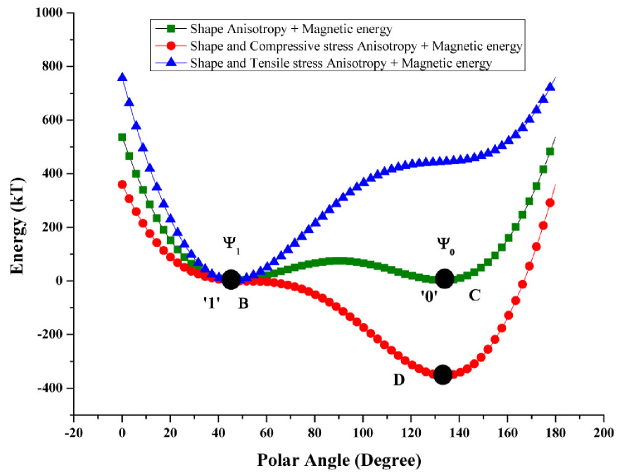
Fig. 2 shows the potential energy profile of the soft magnetostrictive nanomagnet in its own plane ( = 90∘) plotted as a function of the angle subtended by its magnetization vector with the major axis of the ellipse (z-axis). Note that the energy profile has two degenerate minima ( and ) in the absence of stress (i.e. when no voltage is applied between nodes and ). These two states correspond to directions and , respectively, in Fig. 1, which are the two stable magnetization orientations of the soft layer with being anti-parallel to the magnetization of the hard layer and being approximately perpendicular to . Application of sufficient potential difference between and , to generate sufficient stress in the magnetostrictive magnet, transforms the energy profile into a monostable well (with no local minima) located at either or , depending on whether the stress component along the line EE’ is tensile or compressive, i.e. whether node is at a higher potential than node , or the opposite tiercelin ; Giordano . If we apply compressive stress with the right voltage polarity, the system will go to point and the magnetization will point along the corresponding direction very close to . Thereafter, if we withdraw the voltage and stress, the system will go to the nearer energy minimum at point (and not the other minimum at ) because of the potential barrier that exists between and . This happens with 99.999999% probability at room temperature in the presence of thermal noise (see supplementary material). Once it reaches , the system will remain there (since it is an energy minimum) and the magnetization will continue to point along the corresponding direction (making the device non-volatile) until tensile stress is applied [by applying voltage of opposite polarity between and ] to take the system to , thereby changing the magnetization to the other stable direction . Upon withdrawal of the tensile stress, the system will remain in state because the energy barrier between and will prevent it from migrating to . Therefore, the system is non-volatile in either state. By merely choosing the polarity of the voltage between nodes and , we can deterministically visit either state or state and orient the magnetization along either of the two stable states and . In other words, by applying voltages of two different polarities, we can make the MTJ resistance either high or low. The soft nanomagnet’s magnetization (and hence the MTJ resistance) will remain in the chosen state after the voltage is withdrawn. This was used as the basis for deterministically writing the bit 0 or 1 in non-volatile memory, irrespective of what the initial stored bit was tiercelin ; Giordano . Here, we have extended that idea to build a non-volatile universal logic gate (NAND) using a magneto-tunneling junction in the manner of Ref. [ney, ].
The gate works as follows: Let us first assume that the binary logic bits ‘1’ and ‘0’ are encoded in voltage levels and [what determines the minimum value of is discussed later]. The bias voltage is set to = . Every logic operation is preceded by a RESET operation where the two inputs and are set to . During RESET, the potential drop appearing between the terminals and in Fig. 1 is [see supplementary material for a derivation], which generates in-plane tensile stress in the direction of the line joining the two electrodes and in-plane compressive stress in the direction perpendicular to the line joining the two electrodes [we assume that the piezoelectric layer has been poled in the appropriate direction to make a negative voltage drop generate these signs of the in-plane stresses]. This moves the system to point in the energy profile in Fig. 2 where the magnetization vector is in state , nearly anti-parallel to the magnetization of the top magnet (SAF). This makes the resistance of the MTJ ‘high’. When the input voltages are subsequently withdrawn by grounding the inputs and shorting the bias voltage source connected to the Si substrate, drops to nearly zero. Therefore, the stress in the magnet relaxes, but the system remains at point . Consequently, the MTJ is always left in the high resistance state after the RESET step is completed.
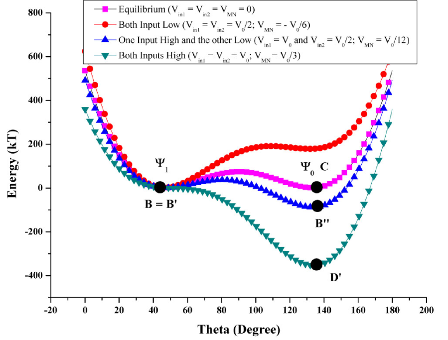
In the logic operation stage, the following scenarios occur: (1) if both inputs are low (i.e. ), then [again, see the supplementary material for a derivation]; (2) if either input is low (i.e. and , or vice versa), then (see supplementary material). The potential energy profiles for these two scenarios are shown in Fig. 3. When both inputs are low, the global energy minimum is at . Since the RESET operation left the system at , the magnetization barely rotates and the MTJ resistance remains high. When one input is high and the other low, the global energy minimum moves to which is closer to the other stable magnetization orientation, but there is still a local energy minimum close to which is separated from by a sufficiently high potential barrier that cannot be crossed. Therefore, the system remains stuck in the metastable state corresponding to the local minimum near and the magnetization does not rotate perceptibly. Hence, once again, the MTJ resistance remains high. After the inputs are removed by grounding and , shorting the bias voltage sources and open-circuiting the bias current source, the strain in the magnet relaxes and the magnetization settles into the only accessible stable state . It remains there in perpetuity, thereby implementing non-volatile logic (memory of the last output state is retained). However, (3) if both inputs are high, then (see supplementary material) and the strain becomes in-plane compressive in the direction of the line joining the two electrodes and in-plane tensile in the direction perpendicular to the line joining the two electrodes. This is sufficient to change the potential energy profile dramatically as shown in Fig. 3. Now the operating point moves to since it becomes the global minimum and there is no local minimum where the system can get stuck. Consequently, the magnetization vector rotates to an orientation nearly perpendicular to the magnetization of the top layer [state ‘’ in Fig. 1(b)]. The resistance of the MTJ then drops by 50% since the resistance is inversely proportional to 1 + , where is the angle between the magnetizations of the top (hard) and bottom (soft) magnets. Since is 180∘ and 90∘ in the high- and low-resistance states, the resistance ratio is , which is roughly 2:1, assuming that the spin injection and detection efficiencies of the magnet-spacer interfaces and are 70% book [if the efficiencies are less than 70%, the logic levels will be encoded in and , where ]. Subsequent removal of the input voltages (by grounding them), drives the system to state where the MTJ resistance remains low, thereby retaining memory of the last output state (non-volatility). The probability of the gate working in this fashion, in the presence of thermal noise, has been calculated rigorously from stochastic Landau-Lifshitz-Gilbert simulations of the magnetodynamics (see supplementary material) and that probability was found to exceed 99.999999% in all cases.
Let us now explain how this translates to NAND logic. Since there is not much electric field in the PZT directly under the MTJ stack Lynch2013 , we can neglect any voltage drop in the PZT between the magnetostrictive magnet and the silicon substrate. Therefore, , where is the resistance of the MTJ stack. The biasing constant current source is set to , where is the resistance of the MTJ in the high-resistance state. Therefore, whenever the MTJ is in the high resistance state, the output voltage is and whenever the MTJ is in the low resistance state, the output voltage is = because [ is the resistance of the MTJ in the low resistance state]. Since the logic bit 1 is encoded in voltage and logic bit 0 is encoded in the voltage level , we find that the output bit is 1 when either input bit is 0, and it is 0 when both inputs are 1. In other words, we have successfully implemented a NAND gate (see the truth table shown in Fig. 1).
Let us now examine if this device fulfills all the requirements of a Boolean logic gate.
Concatenability:
For concatenability, the output voltage of a preceding gate has to be fed directly to the input of a succeeding gate. This requires that , and which is easily achieved by choosing . In the event the logic levels have to be encoded in and (), the resistive network at the input side and have to be re-designed, but this is trivial.
Non-linearity:
Since the MTJ resistance has only two values (high and low), the gate is inherently non-linear behin-aein .
Isolation between input and output:
The output and input terminals are completely isolated. The input is provided to the two contact pads and on the piezoelectric film that generates a strain in the soft layer of the magneto-tunneling junction (MTJ) and changes the MTJ’s resistance. This change in resistance causes the output voltage to change. The output voltage is tapped from the top contact of the MTJ which is electrically isolated from the input terminals. Therefore, this is effectively a three-terminal device – input node, output node and ground (common terminal) – much like a transistor. The input and output nodes are electrically isolated. Note that a change in the input voltage causes a change in the output voltage, but not the other way around. Therefore, the input dictates the output, but not vice versa, resulting in input/output isolation.
There has been extensive discussions about input/output isolation in MTJ-based logic. Ref. [Datta-review, ] discusses input and output states encoded in the magnetization states of two magnets via dipolar coupling, while ref. [m-logic, ] discusses coupling via exchange between input magnetic domains and output. Both dipole and exchange coupling are bidirectional; therefore, there is some chance that the output magnet’s (or domain’s) state can influence the input magnet’s (or domain’s) state. This possibility does not exist in our case at all since there is no bidirectional coupling between input and output.
Gain:
Gain is ensured when the energy to switch the output bit does not come from the input energy, but from an independent power source behin-aein , which, in our case, is the constant current source. Whenever the inputs and end up switching the MTJ resistance, the independent current source switches . The actual gain is the ratio of the swing in the output voltage to the swing in the input voltage. In the supplementary material, we have calculated this gain precisely and show it to be greater than 5 for the parameters we chose. The swing in the output voltage (and hence the gain) can be increased by either increasing the bias current , or the MTJ-resistance . The former approach will increase the energy dissipation and the latter will increase the charging time of the input nodes – both of which will ultimately increase the energy-delay product (see the supplementary material). Thus, there is a trade-off between gain and energy-delay product.
Universal logic:
The gate performs NAND operation which is universal.
Scalability:
Because we do not use magnetic fields to switch specific gates (unlike refs. [cowburn, ] and [ney, ]), but instead use only voltages, we do not have to space gates far apart so that fringing magnetic fields from one gate do not influence the neighbor. As a result, gates can be placed close to each other, thereby increasing the gate density. The gates can scale all the way down to the superparamagnetic limit of the nanomagnets at the operating temperature.
Error-resilience:
Two types of errors afflict non-volatile gate operation: static errors caused by the magnetization of the soft magnetostrictive layer flipping spontaneously between its two stable orientations owing to thermal noise [thereby switching the output bit erroneously in standby state], and dynamic errors that occur (also because of thermal noise) when the output switches to an incorrect state in response to the inputs changing. The static error probability is determined by the energy barrier separating the two stable magnetization states in the soft layer. The minimum barrier height is determined by the magnetic field strength, the dimensions of the magnet and material parameters. In our case, it was 73.1 kT at room temperature (see supplementary material), so the static error probability is 10-32 per spontaneous switching attempt brown . In other words, the retention time of an output bit in the non-volatile logic gate at room temperature will be = 1.771012 years, since the attempt frequency in nanomagnets will very rarely exceed 1 THzgaunt . In other words, the gate is indeed non-volatile. Dynamic gate errors, however, are much more probable and accrue from two sources: (1) thermal noise causing erratic magnetization dynamics that drive magnets to the wrong stable magnetization state resulting in bit error, and (2) complicated clocking schemes that require precise timing synchronization for gate operation and whose failure cause bit errors. The gate in ref. [behin-aein, ] works with Bennett clocking bennett which is predicated on the principle of placing the output magnet in its maximum energy state, and then waiting for the input signal to drive it to the desired one among its two minimum energy states to produce the correct output bit. This strategy is risky since the maximum energy state is also maximally unstable. While perched on the energy maximum, thermal fluctuations can drive the output magnet to the wrong minimum energy state with unacceptably high probability roychowdhury , resulting in unacceptable bit error rates. A later modification behin-aein2 overcame this shortcoming, but at the expense of much increased energy dissipation. Moreover, that logic gate also requires a complicated clocking sequence without which it cannot operate. In contrast, we never place any element of our gate at the maximum energy state (no Bennett clocking) and no complicated clocking sequence is needed.
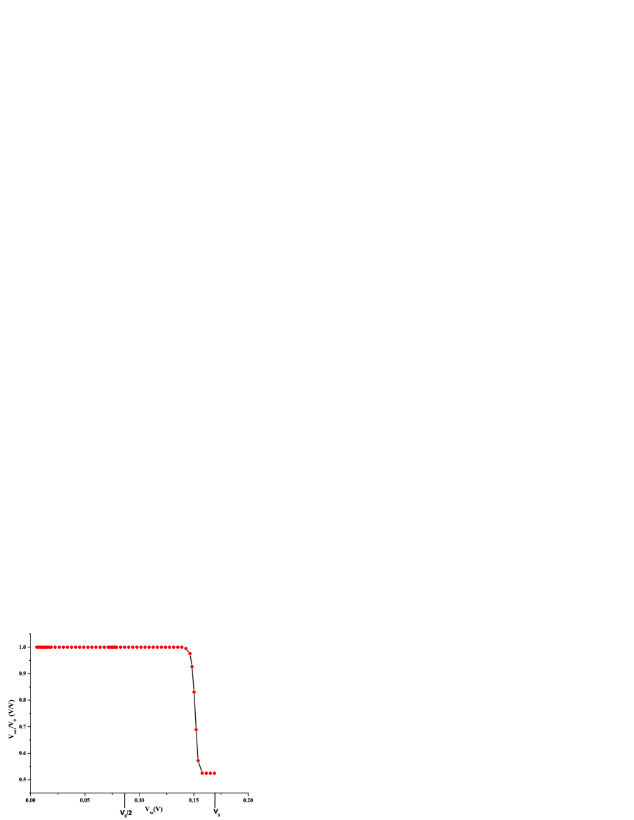
An important consideration for Boolean logic is logic level restoration jackson . If noise broadens the input voltage levels and , making it harder to distinguish between bits 0 and 1, the logic device should be able to restore the distinguishability by ensuring that the output voltage levels are not broadened and remain well separated. For this to happen, the transfer characteristic of the gate (when used as an inverter) must show a sharp transition. We have computed the transfer characteristic ( versus ) by shorting the two inputs (thus making it an inverter) and calculating the output for various values of at room temperature in the presence of thermal noise. The calculation procedure is described in the supplementary section. The characteristic is shown in Fig. 4 and the sharpness of the transition allows for excellent logic level restoration capability.
The proposed gate has unprecedented energy-efficiency that far exceeds that of other non-volatile magnetic NAND gates. There are two contributions to the energy dissipated in this logic gate during a logic operation: direct dissipation associated with switching the gate (which has two components – internal dissipation due to Gilbert damping that occurs in the magnet during magnetization rotation, and energy dissipated in turning on/off the potential (= 56.3 mV) abruptly or non-adiabatically with being the capacitance between the shorted pair of electrodes and the n+-Si substrate), and the indirect dissipation in the resistors , and due to the bias current source . These contributions are computed in the supplementary section and add up to a mere 5176 kT (21.44 aJ) at room temperature. This dissipation is at least an order of magnitude less than in a CMOS transistor embedded in a circuit Datta-review . The switching time, on the other hand, is 1.3 ns, which is almost one order of magnitude longer than that of the CMOS based logic gate. However, the CMOS based gate is volatile while this gate is non-volatile. The time-averaged energy delay product of this gate is 2.7810-26 J-s, which is about two orders of magnitude superior to that of any other magnetic (non-volatile) logic gate and one order of magnitude superior to CMOS. The gate error probability, on the other hand, is 10-8 per logic operation.
Logic gates of this type may have a special niche for medically implanted processors such as pacemakers geddes , wearable electronics starner or devices implanted in an epileptic patient’s brain that monitor brain signals and warn of an impending seizure. They need not be very accurate and therefore a gate error probability of 10-8 may be tolerable. Most importantly, they will dissipate so little energy that they can be powered by the user’s body movements alone and not require a battery kuntal-apl .
Methods
To fabricate the gate, a piezoelectric (PZT) thin film (50 nm thick) is deposited on a conducting n+-Silicon substrate which is grounded through a bias voltage . A skewed MTJ stack is fabricated on top of the PZT film. The bottom layer material is chosen as Terfenol-D because of its large magnetostriction (600 ppm). The magnetostriction is positive which tends to make the magnetization align along the direction of tensile stress and perpendicular to the direction of compressive stress. The angle between the major axes of the two elliptical nanomagnets is determined by the angular separation between and . The current source is connected across the MTJ stack. The magnetostrictive nanomagnet has a major axis of 100 nm, minor axis of 42 nm and thickness of 16.5 nm, which ensures that it has a single ferromagnetic domain.
To evaluate the dynamic error probability, the magnetization dynamics of the soft magnetostrictive magnet induced by stress in the presence of thermal noise is modeled by the stochastic Landau-Lifshitz-Gilbert equation roychowdhury . In the Supplementary section, we present results of simulations to show that if = 0.1689 V, then switching is accomplished in 1.3 ns and the dynamic error probability associated with incorrect switching is less than 10-8 in every gate operation if we keep the voltage on for 1.3 ns. Therefore, the gate can work at a clock frequency of 1/1.3 ns 0.75 GHz with an error probability . Stated succinctly, the probability of the output voltage being low when both inputs are high is % and the probability of it being low when either input is low is . In other words, the NAND gate works with % fidelity. This is unimpressive for transistor-based volatile logic, but it is remarkable for non-volatile magnetic logic gates, which typically have very high error probabilities salehi ; roychowdhury ; bokor . This degree of error-resilience may be sufficient for use in stochastic logic architectures Qian .
SUPPLEMENTARY MATERIAL
In this accompanying supplementary material, we elucidate gate operation, concatenation and choice of the voltage level . We also describe the stochastic Landau-Lifshitz-Gilbert simulations, and calculations of the transfer characteristic and energy dissipation in a gate operation.
I Gate operation
To understand how the RESET, logic and the concatenation schemes work, consider Fig. 5. The nodes and represent the same nodes as in Fig. 1(a) of the main paper and is the voltage drop between these nodes. Therefore, is the voltage drop across the piezoelectric layer that generates strain in the magnetostrictive layer (soft layer of the MTJ) and makes its magnetization rotate. Note that alone determines the MTJ resistance. As established by the energy profiles in the main paper, when is either negative or slightly positive, the hard and soft layers of the MTJ remain magnetized in anti-parallel directions and the MTJ resistance remains high. This high resistance is denoted by . When is positive and sufficiently large in magnitude, the magnetizations of the hard and soft layers become mutually perpendicular and the MTJ resistance drops by a factor of 2 to become .
Since the ratio is 2:1, logic ‘1’ must be encoded in some voltage level and logic ‘0’ in voltage level . This is needed because the logic levels at the output are determined solely by the MTJ resistance.
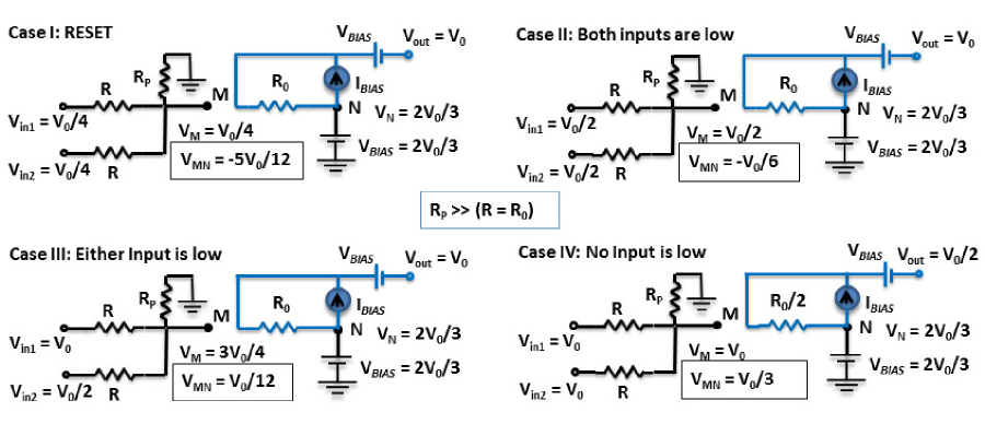
Let us consider the RESET operation that is supposed to leave the MTJ resistance in the high state (Case I in Fig. 5). The input voltages are set to V0/4. The voltage at node is then found by superposition and it is V0/4. Since the bias voltage VBIAS is set to 2V0/3, the voltage at node is always fixed at 2V0/3. Therefore, , which is the voltage drop across the PZT thin film, becomes V0/4 - 2V0/3 = -5V0/12. This negative voltage generates a stress profile in the magnetostrictive layer that leaves its magnetization pointing anti-parallel to that of the the hard (SAF) layer of the MTJ (close to ). Therefore, the MTJ resistance is left high at by the RESET step.
Note that the voltage drop between the bottom (soft) layer of the MTJ and node is almost zero since the metallic layer shorts out the electric field underneath it in the PZT Lynch2013 . Therefore, by applying Kirchoff’s voltage law in the output loop, we find that
| (1) |
since is set to . Because after the RESET stage, after the RESET operation has been completed.
Next consider the logic operation stage when both inputs are low (Case II). Since = = , is [use superposition] and thus (= ) is -. This negative voltage once again generates a stress profile in the magnetostrictive magnet that leaves the magnetizations of the hard and soft layers of the MTJ anti-parallel and the MTJ resistance high. Therefore, from Equation (1), . In other words, when both inputs are ‘0’, the output is ‘1’.
When one input is high and the other low (Case III), = and = (the case where = and = is completely equivalent). The voltage at node , , is now [again, by superposition], which makes . The stress profile in the magnetostrictive layer now changes, but not enough to rotate its magnetization by overcoming the shape anisotropy energy barrier of the elliptical magnet. Therefore, MTJ resistance remains high at and the output voltage remains high at . In other words, when one input is ‘1’ and the other is ‘0’, the output is ‘1’.
When both inputs are high (Case IV), = = . In that case, VM changes to [use superposition], and becomes /3. The stress generated by this magnitude of in the magnetostrictive layer of the MTJ is sufficient to overcome the shape anisotropy barrier. As a result, the magnetization of the soft layer of the MTJ now rotates by 90∘, placing it approximately perpendicular to that of the hard layer. Therefore, the MTJ’s resistance drops to and [from Equation (1)] the output voltage drops to . Thus, when both inputs are ‘1’, the output is ‘0’. All this implements NAND logic.
Note that the output voltage levels encoding bits ‘1’ and ‘0’ are and which are also the input voltage levels encoding bits ‘1’ and ‘0’. Therefore, the output of one stage can be directly fed to the next stage as input without requiring additional hardware for amplification or level shifting. That makes this construct concatenable.
II Choice of voltage level
In order to choose the value of (which ultimately determines the amount of dissipation, switching delay and energy-delay product), we have to ensure that compressive stress generated by is sufficient to overcome the shape anisotropy barrier in the elliptical magnetostrictive layer and rotate its magnetization, but compressive stress generated by is not. The amount of stress generated by a certain voltage, and the effective shape anisotropy barrier in the presence of the permanent magnetic field, depend on many parameters such as the strength of the magnetic field, the shape and size of the magnetostrictive layer, the electrode size and placements, the piezoelectric layer thickness, and the piezoelectric and magnetostrictive materials. For the choices we made, we found from stochastic Landau-Lifshitz-Gilbert simulations of magnetodynamics in the presence of room-temperature thermal noise Roy2012 that a compressive stress of -30 MPa rotates the magnetization with greater than 99.999999% probability (and switches the MTJ resistance from high to low) in the presence of room-temperature thermal fluctuations, while a compressive stress of -7.5 MPa (one-fourth of -30 MPa) has less than 10-8 probability of rotating the magnetization and switching the MTJ resistance. Therefore, needs to generate a stress of -30 MPa (compressive strain is negative). The material chosen for the magnetostrictive material is Terfenol-D because of its large magnetostriction. From the Young’s modulus of Terfenol-D, we calculated that the strain required to generate a stress of -30 MPa is -3.7510-4. To generate this amount of strain, the strength of the electric field in the PZT between the shorted electrodes and the n+-Si substrate should be 1.126 MV/m (interpolated from the results in Ref. [Lynch2013, ]). This value is well below the breakdown field of PZT. We assume that the PZT layer thickness is 50 nm (easily achievable); hence, the voltage needed to generate the strain of -3.7510-4 will be 1.126 MV/m 50 nm = 56.3 mV. Hence, = 0.1689 V.
III Stochastic Landau-Lifshitz-Gilbert (LLG) simulations
The error probability associated with gate operation, the internal energy dissipated during switching, and the switching delay – all in the presence of room-temperature thermal noise – are calculated from the stochastic Landau-Lifshitz-Gilbert (LLG) equation111The LLG equation is based on the macrospin assumption which assumes that the entire domain in a single-domain nanomagnet rotates coherently and all the spins in it rotate in unison, collectively acting as one giant classical spin. In general, the macrospin assumption works fairly well for elliptical shaped nanomagnets and this has been verified by comparison with micromagnetic simulations (OOMMF) mamun .. We first write expressions for the various contributions to the potential energy of the magnetostrictive layer and then find the effective torques acting on the magnetization vector due to these contributions as well as the random torque due to thermal noise. These torques rotate the magnetization vector. The entire procedure is described next.
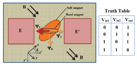
We reproduce Fig. 1(b) from the main paper as Fig. 6 and define our coordinate system such that the magnet’s easy (major) axis lies along the z-axis and the in-plane hard (minor) axis lies along the y-axis (see also Fig. 1(a) in main paper). Application of a positive/negative voltage between the electrode pair and the conducting n+-Si substrate generates biaxial strain leading to compression/expansion along the z′-axis and expansion/compression along the y′-axis Lynch2013 . The latter two axes are the axes of and . The angle between the z- and z′ axes is , which is therefore the angle between the major axes of the hard and soft elliptical magnets.
To derive general expressions for the instantaneous potential energies of the nanomagnet due to shape-anisotropy, stress-anisotropy and the static magnetic field, we used the primed axes of reference (x′, y′, z′) and represented the magnetization orientation of the single-domain magnetostrictive magnet in spherical coordinates with representing the polar angle and representing the azimuthal angle. The magnitude of the magnetization is invariant in time and space owing to the macrospin assumption.
Using the rotated coordinate system (see Fig. 6), the shape anisotropy energy of the nanomagnet can be written as,
| (2) |
where and are respectively the instantaneous polar and azimuthal angles of the magnetization vector in the rotated frame, is the saturation magnetization of the magnet, , and are the demagnetization factors that can be evaluated from the nanomagnet’s dimensions Beleggia2005 , is the permeability of free space, and is the nanomagnet’s volume.
The potential energy due to the static magnetic flux density applied along the in-plane hard axis is given by
| (3) |
The stress anisotropy energy is given by
| (4) |
where is the magnetostriction coefficient, is the Young’s modulus, and is the strain generated by the applied voltage at the instant of time . We only consider the uniaxial strain along the line joining the two electrodes, but the strain is actually biaxial resulting in tension/compression along that line and compression/tension along the perpendicular direction. The torques due to these two components add. Therefore, we underestimate the stress anisotropy energy, which makes all our figures conservative.
We neglect any contribution due to the dipolar interaction of the hard magnet since the use of the synthetic anti-ferromagnet makes it negligible.
The total potential energy of the nanomagnet at any instant of time is therefore
| (5) |
The above result is used to plot the energy profiles in the main paper as a function of for under various scenarios.
We follow the standard procedure to derive the time evolution of the polar and azimuthal angles of the magnetization vector in the rotated coordinate frame under the actions of the torques due to shape anisotropy, stress anisotropy, magnetic field and thermal noise.
The torque that rotates the magnetization of the shape-anisotropic magnet in the presence of stress can be written as
| (6) | |||||
where is the normalized magnetization vector, quantities with carets are unit vectors in the original frame of reference, and
At non-zero temperatures, thermal noise generates a random magnetic field with Cartesian components that produces a random thermal torque which can be expressed as Roy2012
where
| (7) |
In order to find the temporal evolution of the magnetization vector under the vector sum of the different torques mentioned above, we solve the stochastic Landau-Lifshitz-Gilbert (LLG) equation:
| (8) |
From the above equation, we can derive two coupled equations for the temporal evolution of the polar and azimuthal angles of the magnetization vector:
| (9) | |||||
| (10) | |||||
Solutions of these two equations yield the magnetization orientation at any instant of time . Since the thermal torque is random, the solution procedure involves generating switching trajectories by starting each trajectory with an initial value of () and finding the values of these angles at any other time by running a simulation using a time step of t = 1 ps and for a sufficiently long duration. At each time step, the random thermal torque is generated stochastically. The time step is equal to the inverse of the maximum attempt frequency of demagnetization due to thermal noise in nanomagnets gaunt . The duration of the simulation is always sufficiently long to ensure that the final results are independent of this duration, and they are also verified to be independent of the time step.
The permanent magnetic field ( = 0.14 T) applied along the +y- direction (hard axis of the magnet) makes the two stable states of the soft magnet’s magnetization align along ( = 46.9∘) and ( = 133.1∘) leaving a separation angle of 86.2∘ (Fig. 6) between them. Thermal noise however will make the magnetization of the soft magnet fluctuate around either of these two orientations and in order to determine the thermal distribution around (which is where the RESET operation leaves the magnetization at), we solve the last two equations in the absence of any stress by starting with the initial state = 46.9∘ and = 90∘ and obtaining the final values of and by running the simulation for a long time. This process is repeated 100 million times. A histogram is then generated from these 100 million trials for the final values of and , which yields the thermal distribution around .
To study the switching dynamics under the influence of stress, we generate 100 million switching trajectories in the stressed state of the magnet by solving Equations (9) and (10), again using a time step of 1 ps. This time the initial magnetization orientation for each of the 108 trajectories is chosen from the thermal distributions generated in the previous step with the appropriate weightage since the RESET step always leaves the magnetization around state . The simulation is continued for 1.5 ns. We find that when the stress is either tensile (+15 MPa corresponding to ), or compressive but weak (-7.5 MPa corresponding to ), the magnetization’s polar angle returns to within 4∘ of ( = 46.9∘) in 1.3 ns or less for every one of the 108 trajectories. After 1.3 ns, the stress is removed abruptly and the simulation is continued for an additional 0.2 ns to ensure that the final state does not change. It did not change for any of the 108 trajectories. This procedure tells us that when the inputs to the logic gate are both low, or one is high and the other is low, the magnetization of the soft layer of the MTJ does not rotate and the MTJ resistance remains high with 99.999999 probability. This fulfills the requirements of the NAND gate with 99.999999 probability.
In the case of one input low and one input high, what prevents rotation from to is the energy barrier of 36 kT between these two states as discussed in the main paper. This barrier is high enough to reduce the unintended switching probability to below 10-8.
When both inputs are high, a compressive stress of -30 MPa is generated in the magnetostrictive magnet. Once again, we pick the initial orientations of the magnetization from the thermal distribution around which is where the RESET step leaves the magnet at, and generate 100 million switching trajectories as before. This time approaches within 4∘ of final state ( = 133.1∘) in 1.3 ns or less. We continue the simulation for an additional 0.2 ns to confirm that once the magnetization reaches the vicinity of , it settles around that orientation and does not return to the neighborhood of the initial orientation . We repeated this procedure for 108 times and found that every single switching trajectory behaved in the above manner. Therefore, we conclude that when the inputs to the logic gate are both high, the magnetization of the soft layer of the MTJ does rotate and the MTJ resistance goes low with 99.999999 probability. That fulfills the remaining requirement of the NAND gate with 99.999999 probability.
IV Transfer characteristics of NAND gate
When the two inputs of a NAND gate are shorted, it behaves like a NOT gate (inverter). If the input voltage to the inverter is between and (i.e. the compressive stress is between -7.5 MPa and -30 MPa), the energy profile becomes such that the magnetization of the soft layer may rotate to an intermediate state between and and fluctuate around that orientation because of thermal noise, as long as the stress is kept on. We can time-average over the fluctuations to determine the ‘steady-state’ mean orientation at that input voltage and thence calculate and . In order to do this, we calculate the stress generated by the corresponding to the input voltage and run the stochastic Landau-Lifshitz-Gilbert simulation to determine the mean steady-state magnetization orientation of the soft layer and from that the mean values of and . The purpose of this exercise is to find the transfer characteristic versus at room temperature. This characteristic is shown in the main paper and shows a sharp transition. The transition range is from 142.69 mV to 157.7 mV (a range of 15.01 mV) of input voltage whereas the logic levels are 88.67 mV and 168.9 mV. This portends excellent logic level restoration capability. In the high state, the input voltage can drift down by 11.2 millivolts and still produce the correct output state, while in the low state, the input voltage can drift up by 54.02 millivolts and still produce the correct output state.
One can also calculate an effective “gain” from the transfer characteristic. We define the gain as and this quantity is (168.9 - 88.67)/15.01 = 5.34.
V Energy Dissipation
The energy dissipated in the NAND gate has two components: direct (associated with the switching action) and indirect (caused by the peripherals unavoidably). The direct dissipation has two contributions: internal dissipation due to Gilbert damping that occurs while the magnetostrictive layer’s magnetization switches (rotates) and energy dissipated in turning on/off the potential abruptly or non-adiabatically during the logic operation stage (where is the capacitance between the shorted pair of electrodes and the n+-Si substrate). We will address the indirect dissipation later, but first we address the direct contribution.
The energy dissipated due to Gilbert damping in a magnet is given by behin-aein ; sun2005
| (11) |
where is the switching delay (counted between the time the magnetization leaves the vicinity of and arrives within 4∘ polar angle of ) and is the power dissipation and can be expressed as
| (12) |
where is the vector sum of the torques due to shape anisotropy, stress anisotropy and bias magnetic field (the thermal torque does not dissipate energy). The energy dissipation is obviously different for different switching trajectories because of the integration over time, and we have found that the mean dissipation is 316 kT at room temperature. This calculation overestimates the energy dissipation slightly, but that only makes our figures conservative.
The next component is the dissipation. We have electrodes of dimensions 80 nm 80 nm and the thickness of the PZT layer is 50 nm. Thus, the capacitance between either electrode and the silicon substrate is C = 1.13 fF, assuming that the relative dielectric constant of PZT is 1000. The maximum value of the voltage is (= 56.3 mV). Since we have a pair of electrodes, the dissipation will be roughly twice (1/2). We calculated that value as 865 kT. Therefore, the total direct disssipation is at most 316 + 865 = 1181 kT = 4.9 aJ
VI Charging time
The output of one stage charges the input of the next stage. We need to calculate the time it takes for the input of the next stage to charge up after the output of the preceding state changes. This should be much shorter than the gate delay.
The PZT thin film of the successor gate acts as a capacitor whose one end is connected to bias voltage source and the other is connected via passive resistors and to the output of the preceding stage. The equivalent charging circuit is shown in the left panel of Fig. 7 where C1 represents the capacitance due to the PZT layer underneath the MTJ in the preceding gate and C2 is the capacitance due to the PZT layer underneath the metal electrodes in the successor gate. The resistor RMTJ represents the resistance of the MTJ stack of the preceding stage. The other resistors are the passive resistances at the input of the successor gate.
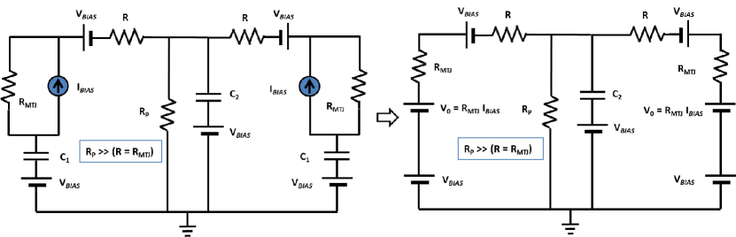
In the right panel of the Fig. 7, we have converted the Norton’s equivalent circuit for the current source to Thevenin’s equivalent circuit for a voltage source. We have shorted the capacitor C1 for the following reason. There is no electric field underneath the MTJ and the voltage drop across this region is almost zero. Since the initial and final voltages on this capacitor are zero, the charging/discharging of this capacitor can be ignored and we will treat it as a virtual short.
The charging time constant of the circuit will therefore be
| (13) |
We choose , which makes Req (R + R. We then select = 80 k and RP = 10 G. This makes the charging time constant 180 picoseconds where C2 is 21.13 fF (due to two metal electrodes). Compare this time with the magnet switching time of 1.3 ns. Since this time is much shorter than the magnet switching time, we can approximate the stress application and withdrawal as virtually ‘instantaneous’.
VII The bias current
The bias current is given by = 0.1689/80 k = 2.11 A. This current is passed through the soft magnet whose lateral area is nm2, resulting in a current density of 0.064 MA/cm2, which is far below the critical current for switching a magnet due to spin transfer torque or domain wall motion. Therefore, the bias current source cannot cause any unwanted spurious switching.
VIII Indirect energy dissipation
Fig. 8, derived from Fig. 7, shows the equivalent circuit for calculating the indirect power dissipation. Once charged up, the capacitor becomes an open circuit and the equivalent voltage source V0 (due to the bias current source ) now drives a current through the resistors, causing power dissipation that does not aid the switching, but is unfortunately unavoidable.
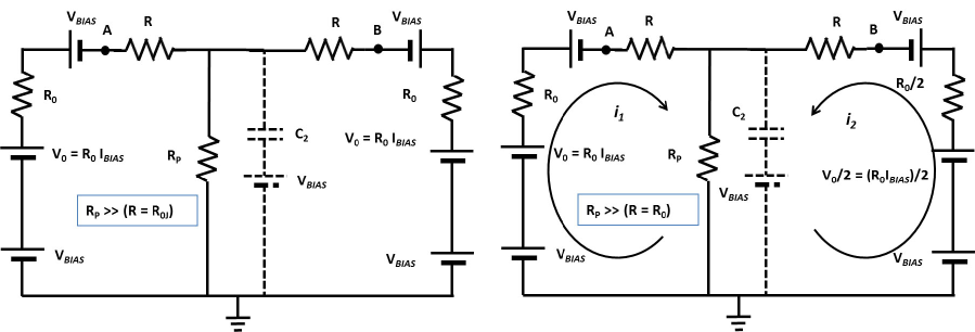
If both inputs are at the same state (i.e. both are high, both are low, or in RESET) the voltage sources (both , /2, or /4) drive a current through the series resistors and and a current 2 through the parallel resistance where . This causes power dissipation given by
| (14) |
The maximum value of V0 is 0.1689 V; hence, the indirect energy dissipation over the gate delay is Eindirect1 = Pindirect1 tS 3.7 zJ which is negligible (tS is the switching time).
When either input is low, one voltage source is at and other is at /2. The MTJ resistances in the two branches are and . Currents flow through the series resistors and in the left loop, and and in the right loop, as well as the parallel resistor , as shown in the right panel of Fig. 8. By solving the circuit in the right panel, we find that the currents i1 and i2 are 301.612 nA and -301.6 nA respectively. The corresponding power dissipations in due to i1, and in due to i2, are 14.55 nW and 10.9 nW, respectively. The current that flows through the resistor RP is , which is very small (12 pA) and hence the power dissipation in this resistor is negligible. Therefore, the total indirect energy dissipation Eindirect2 is (14.55 + 10.9) nW 1.3 ns = 33.08 aJ (7986 kT). We can clearly see that Eindirect2 is much larger than Eindirect1 when either input is low. Fortunately, in a random input stream, this situation arises 50% of the time. Hence, the time averaged energy dissipation will be 16.54 aJ or 3993 kT.
Consequently, in one cycle of a gate operation, the time-averaged energy dissipation is roughly 4.9 + 16.54 = 21.44 aJ = 5176 kT. The time averaged energy-delay product is 21.44 aJ 1.3 ns = 2.7810-26 J-sec. This figure is almost two orders of magnitude smaller than that of any other magnetic non-volatile logic gate proposed until now (to our knowledge) and one order of magnitude smaller than that of CMOS gates.
IX A few fundamental considerations
This logic gate is switched by charging a capacitor which generates strain in a piezoelectric and that strain switches the MTJ resistance. Charging a capacitor involves moving an amount of charge in and out of a region in some time , resulting in a charging current and an associated energy dissipation where bandy_nanoscience . The energy-delay product is . In our gate, the quantity which is equal to is 2 1.13 fF 56.3 mV = 0.127 fC = 795 electronic charge. In contrast, when magnets are switched with spin polarized current directly, the amount of charge moved is at least 20,000 Datta-review . This may portend a fundamental advantage of voltage-controlled straintronic switching over current-induced switching of magnets.
The energy-delay product should be (0.127 fC)2 80 k = 1.310-27 J-sec. This is the energy-delay product associated with just charging and discharging the gate in response to inputs. There are additional sources of dissipation in the gate due to internal losses and additional delay due to magnet switching. These additional components make the actual energy-delay product roughly an order of magnitude larger in our case.
References
- (1) Cowburn, R. P. & Welland, M. E. Room temperature magnetic quantum cellular automata. Science 287, 1466 - 1468 (2000).
- (2) Ney, A., Pampuch, C., Koch, R. & Ploog, K. H. Programmable computing with a single magnetoresistive element. Nature 425, 485 - 487 (2003).
- (3) Behin-Aein, B., Datta, D., Salahuddin, S. & Datta S., Proposal for an all-spin logic device with built-in memeory. Nature Nanotech. 5, 266 - 269 (2010).
- (4) Srinivasan, S., Sarkar, A., Behin-Aein, B. & Datta, S. All-spin logic device with in-built non-reciprocity. IEEE Trans. Magn. 47 4026 - 4032 (2011).
- (5) Waser, R. (ed.) Nanoelectronics and Information Technology, Ch. III (Wiley-VCH, 2003).
- (6) Spedalieri, F. M., Jacob, A. P., Nikonov D. E. & Roychowdhury, V. P. Performance of magnetic quantum cellular automata and limitations due to thermal noise. IEEE Trans. Nanotech. 10, 537 - 546 (2011).
- (7) Salehi-Fashami, M., Munira, K., Bandyopadhyay, S., Ghosh, A. W. & Atulasimha, J. Switching of dipole coupled multiferroic nanomagnets in the presence of thermal noise: reliability analysis of hybrid spintronic-straintronic nanomagnetic logic. IEEE Trans. Nanotech. 12, 1206 - 1212 (2013).
- (8) Carlton, D. et al. Investigation of defects and errors in nanomagnetic logic circuits. IEEE Trans. Nanotech. 11, 760 - 762 (2012).
- (9) Lee, S., Choa, S., Lee, S. & Shin, H. Magneto-logic device based on a single-layer magnetic tunnel junction. IEEE Trans. Elec. Dev. 54 2040-1044 (2007).
- (10) Wang, J., Meng, H. & Wang J-P. Programmable spintronics logic device based on a magnetic tunnel junction element. J. Appl. Phys. 97, 10D509 (2005).
- (11) Roy, K. Ultra-low-energy non-volatile straintronic computing using single multiferroic composites. Appl. Phys. Lett. 103, 173110 (2013).
- (12) Bandyopadhyay, S. & Atulasimha, J. Comment on “Ultra-low-energy non-volatile straintronic computing using single multiferroic composites” Appl. Phys. Lett. 105, 176101 (2014).
- (13) Salehi-Fashami, M., Bandyopadhyay, S. & Atulasimha, J. Magnetization dynamics, throughput and energy dissipation in a universal multiferroic nanomagnetic logic gate with fan-in and fan-out. Nanotechnology 23, 105201 (2012).
- (14) Alam, M. T. et al. On-chip clocking for nanomagnetic logic devices. IEEE Trans. Nanotech. 9, 348 - 351 (2010).
- (15) Sharad, M., Yogendra, K., Gaud, A., Kwon, K. W. & Roy, K. Ultra-high density, high-performance and energy-efficient all spin logic. arXiv:1308:2280 [cond-mat:mes-hall].
- (16) Behin-Aein, B., Sarkar, A., Srinivasan, S. & Datta, S. Switching energy-delay of all spin logic devices. Appl. Phys. Lett. 98, 123510 (2011).
- (17) Nikonov, D. E. & Young, I. A. Overview of beyond CMOS devices and uniform methodology for their benchmarking. Proc. IEEE 101, 2498 (2013).
- (18) Datta, S., Diep, V. Q. & Behin-Aein, B. What constitutes a nanoswitch? A perspective. arXiv:1404.2254.
- (19) Tiercelin, N., Dusch, Y., Preobrazhensky, V., & Pernod, P. Magnetoelectric memory using orthogonal magnetization states and magnetoelastic switching. J. Appl. Phys. 109, 07D726 (2011).
- (20) Giordano, S., Dusch, Y., Tiercelin, N., Pernod, P., & Preobrazhensky, V. Combined nanomechanical and nanomagnetic analysis of magnetoelectric memories. Phys. Rev. B 85, 155321 (2012).
- (21) Cui, J. et al. A method to control magnetism in individual strain-mediated magnetoelectric islands. Appl. Phys. Lett. 103, 232905 (2013).
- (22) Li, P. et al. Electric field manipulation of magnetization rotation and tunneling magnetoresistance of magnetic tunnel junctions at room temperature. Adv. Mater. 26, 4320 (2014).
- (23) Bandyopadhyay, S & Cahay, M. Introduction to Spintronics (CRC Press, Boca Raton, 2008).
- (24) Bromberg, D. M., Morris, Pileggi, L & Zhu, J-G. Novel STT-MTJ device enabling all-metallic logic circuits. IEEE Trans. Magn. 48, 3215 (2012).
- (25) Brown, W. F. Thermal fluctuations of a single-domain particle. Phys. Rev. 130, 1677 - 1685 (1963).
- (26) Gaunt, P. The frequency constant for thermal activitation of a ferromagnetic domain wall. J. Appl. Phys. 48, 3470 (1977).
- (27) Bennett, C. H. The thermodynamics of computation - A review. Intl. J. Theor. Phys. 21, 905 - 940 (1982).
- (28) Hodges, D. A. & Jackson, H. G. Analysis and Design of Digital Integrated Circuits, 2nd. edition, (McGraw Hill, New York, 1988).
- (29) Geddes, L. A. Historical highlights in cardiac pacing. IEEE Engineering in Medicine and Biology Magazine 12 - 18, June 1990.
- (30) Starner, T. Human powered wearable computing. IBM Systems Journal 35, 618 - 629 (1996).
- (31) Roy, K., Bandyopadhyay, S., & Atulasimha, J. Hybrid spintronics and straintronics: A magnetic technology for ultra low energy computing and signal processing. Appl. Phys. Lett. 99, 063108 (2011).
- (32) Qian, W., Li, X., Riedel, M., D., Bazargan, K., & Lilja, D. J. An architecture for fault-tolerant computation with stochastic logic. IEEE Trans. Comp. 60, 93 (2011).
- (33) Roy, K., Bandyopadhyay, S. & Atulasimha, J. Energy dissipation and switching delay in stress-induced switching of multiferroic nanomagnets in the presence of thermal fluctuations. J. Appl. Phys. 112, 023914 (2012).
- (34) Al-Rashid, Md. M., Bhattacharya, D., Bandyopadhyay, S. & Atulasimha, J. The effect of nanomagnet geometry on reliability, energy dissipation and clock speed in strain-clocked dipole-coupled nanomagnetic logic. submitted to IEEE Trans. Elec. Dev.
- (35) Beleggia, M., De Graef, M., Millev, Y. T., Goode, D. A. & Rowlands, G. Demagnetization factors for elliptic cylinders J. Phys. D: Appl. Phys. 38, 3333 (2005).
- (36) Sun, Z. Z. & Wang, X. R., Fast magnetization switching of Stoner particles: A nonlinear dynamics picture. Phys. Rev. B. 71, 174430 (2005)
- (37) Bandyopadhyay, S. Power dissipation in spintronic devices: A general perspective. J. Nanosci, Nanotechnol. 7, 168 (2007).
Acknowledgement
This work is supported by the US National Science Foundation (NSF) under grants ECCS-1124714 and CCF-1216614 and by Semiconductor Research Company (SRC) under NRI task 2203.001. J. A’s work is also supported by NSF CAREER grant CCF-1253370.
Author contributions
A. K. B. carried out the stochastic Landau-Lifshitz-Gilbert simulations to evaluate the error probability. S. B and J. A. came up with the idea and verified the simulation results. All authors contributed to writing the paper.
Competing financial interests
The authors declare no competing financial interests.