Strain-induced conduction gap in vertical devices
made of twisted graphene layers
Abstract
We investigate the effects of uniaxial strain on the transport properties of vertical devices made of two twisted graphene layers, which partially overlap each other. We find that because of the different orientations of the two graphene lattices, their Dirac points can be displaced and separated in the space by the effects of strain. Hence, a finite conduction gap as large as a few hundred meV can be obtained in the device with a small strain of only a few percent. The dependence of this conduction gap on the strain strength, strain direction, transport direction and twist angle are clarified and presented. On this basis, the strong modulation of conductance and significant improvement of Seebeck coefficient are shown. The suggested devices therefore may be very promising for improving applications of graphene, e.g., as transistors or strain and thermal sensors.
pacs:
xx.xx.xx, yy.yy.yy, zz.zz.zzThe continuing interest in graphene, a two-dimensional (2D) monolayer arrangement of carbon atoms, as conducting material is one of the most striking trends of research in solid-state and applied physics over the last decade neto09 ; ywu013 ; yazy10 ; bala11 ; shar13 ; novo12 ; schw10 . It is due in particular to the specific band structure of this material, i.e. with gapless conical shape at the six edge corners of the hexagonal Brillouin zone and the Dirac character of low-energy excitations, which leads to many peculiar effects as relativistic-like behavior of charge carriers, finite value of the conductivity at zero density, unusual quantum Hall effect, etc neto09 . It is due also to outstanding properties as high carrier mobility, small spin-orbit coupling, high thermal conductivity and excellent mechanical properties, which make it very promising for a broad range of applications. However, in the view of operation of electronic devices, graphene still has serious drawbacks associated with the lack of an energy bandgap in its electronic structure. In particular, graphene transistors have low ON/OFF ratio and poor current saturation meri08 . Many efforts of bandgap engineering in graphene have been made to solve these issues. For instance, the techniques as cutting 2D graphene sheet into narrow nanoribbons yhan07 , depositing graphene on hexagonal boron nitride (hBN) substrate khar11 , nitrogen-doped graphene lher13 , applying an electric field perpendicularly to Bernal-stacking bilayer graphene zhan09 , graphene nanomeshes jbai10 , using hybrid graphene/hBN fior12 or vertical graphene channels brit12 have been explored. Though being certainly promising options, each of these technique still has its own issues. Hence, the bandgap engineering is still a timely and desirable topic at the moment for the development of graphene in nanoelectronics.
Besides these points mentioned above, graphene is also an attractive material for flexible electronics since it is able to sustain a much larger (i.e., shar13 ) strain than other semiconductors. Recently, some techniques garz14 ; shio14 to generate extreme strain in graphene in a controlled and nondestructive way have been also explored. Interestingly, strain engineering has been suggested to be an approach to modulate efficiently the electronic structure of graphene nanomaterials. On this basis, many interesting electrical, optical and magnetic properties induced by strain have been investigated, e.g., see refs. pere09a ; pere09b ; cocc10 ; yalu10 ; kuma12 ; baha13 ; hung14a ; chun14 ; pere10 ; gxni14 ; guin10 ; tlow10 ; zhai11 . Remarkably, although the slightly strained (i.e., a few percent) 2D graphene remains semimetallic pere09b , strain has been demonstrated as a technique for strongly improving the applications of some particular graphene channels, for instance, graphene nanoribbons with a local strain yalu10 ; baha13 , graphene with grain boundaries kuma12 and graphene strain junctions hung14a ; chun14 .
Recently, the interest of the graphene community has been also oriented toward the investigation of specific graphene systems, named twisted few-layer graphene lattices. They are actually few-layer graphene lattices where one layer is rotated relative to another layer by an arbitrary angle and can form a Moiré pattern. These graphene lattices often appear in the thermal decomposition of the C-face of SiC or in the copper-assisted growth using the chemical vapor deposition method, e.g., see refs. heer07 ; hass08 ; caro11 ; luic11 ; have12 ; cclu13 . In the twisted graphene bilayer, the bandstructure changes dramatically sant07 ; lais10 ; guli10 , compared to that of monolayer or Bernal/AA stacking bilayer systems. In addition to the existence of linear dispersion in the vicinity of K-points, saddle points emerge at the crossing of Dirac cones, yielding van Hove singularities in the density of states at low energies, and the Fermi velocity to be remarkably renormalized. Moreover, the phonon transport in these systems also exhibits a strong dependence on the twist angle coce13 . Motivated by recent studies kuma12 ; hung14a ; chun14 of the strain effects to generate/modulate the conduction gap in graphene channels, we investigate in this work the effects of uniaxial strain on the charge transport in vertical devices made of two twisted graphene layers as schematized in Fig. 1. The idea is as follows. In any hetero-channels made of different graphene sections where their Dirac cones are located at different positions in the space, the transmission probability (and hence conductance/current) shows finite energy gaps, i.e., conduction gaps, even though these graphene sections are still metallic (similarly, see the detailed explanation in kuma12 ; chun14 ). This feature is also expected to be observed here because the graphene lattices in the left and right sides have different orientations and hence their electronic structures should be, in principle, different when a strain is applied. Moreover, compared to the strain heterochannels hung14a ; chun14 and vertical devices brit12 previously studied, the advantages of these devices come from the use of a uniform strain and graphene materials only, which can make it a quite simple option for the fabrication process.
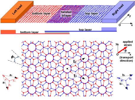
For the investigation of charge transport in the proposed devices, we employed atomistic tight-binding calculations as in pere09b ; lais10 ; sant12 ; hung14a ; chun14 . Here, we assume that: (i) two (bottom and top) graphene sheets partially overlap each other and the transport (i.e., Ox) direction is perpendicular to this overlap section as shown in Fig. 1; (ii) the top sheet is rotated relative to the bottom one by a commensurate angle ; (iii) a uniformly uniaxial strain is applied in the in-plane direction with an arbitrary angle with respect to the transport direction. The commensurate angles are determined by sant12 , where n and m are coprime positive integers. The primitive vectors shown in Fig. 1 are determined as follows: and if gcd(n,3) = 1; and if gcd(n,3) = 3 [where gcd(p,q) is the greatest common divisor of p and q]. For simplicity, throughout the work, unless otherwise stated the transport direction is chosen to be parallel to the vector . The strain causes changes in the bond vector according to with the strain tensor
where represents the strain and is the Poisson ratio blak70 . Taking into account the strain effects, the hopping parameters of tight binding Hamiltonian are adjusted accordingly as in pere09b . To compute the transport quantities (transmission probability and conductance) and extract the value of conduction gap, we used the non-equilibrium Green’s function technique and the bandstructure analysis, as described in hung14a ; chun14 . The conduction gap mentioned here is essentially the energy window within which the Fermi energy can be varied (e.g., by applying and tuning a back gate voltage) and the channel remains insulating. Note that due to the lattice symmetry, the twisted graphene bilayer lattices with and are equivalent while the applied strain of angle is identical to that of . It hence limits our investigation to and .
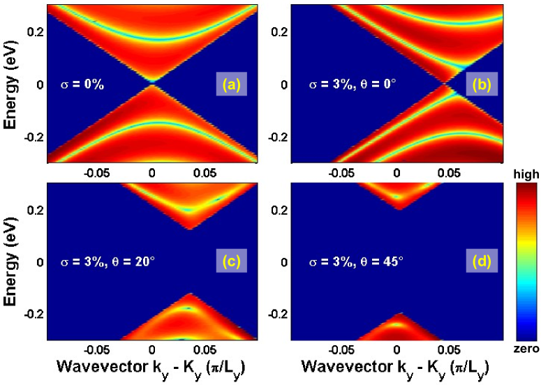
In Fig. 2, we present maps showing the main effects of strain on the transmission coefficient of considered devices in the case of (i.e., ). First, the device remains metallic with a zero conduction gap in the case of unstrained layers (see Fig. 2(a)). This is because the Dirac cones of graphene sections in the left and right sides are still located at the same position, i.e., at the K-point. The strain can induce a displacement of Dirac cones from the K-point pere09b ; chun14 and a finite gap can open in the device if the Dirac cones of two such graphene sections are separated along the -direction, similarly to what was explained in chun14 . Therefore, the transport picture is dramatically changed as shown in Figs. 2(b,c,d). In Fig. 2(b), although the Dirac cones are displaced, the device is still metallic with a zero conduction gap. This is essentially explained by the fact that the system is symmetric with respect to the overlap region (i.e., the Oy direction) even the strain of 3 with is applied. Because of this symmetry, the Dirac cones of left and right sections are still located at the same point, which explains the zero gap observed. This symmetry can be broken when the direction of applied strain changes, leading to the opening of a finite conduction gap (see Figs. 2(c,d)). Indeed, finite gaps of 240 meV and 390 meV are achieved for the strain angles and , respectively. Thus, these data show two important features: (i) the strain can induce a finite conduction gap in the device under study and (ii) besides the strain strength, the gap is strongly dependent on the strain direction. Similar features have been also reported in chun14 for monolayer graphene strain junctions.
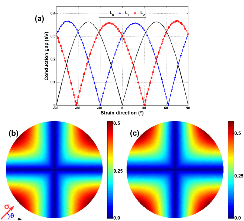
In Fig. 3, we display a picture showing the properties of conduction gap in the device discussed above with respect to the strain strength, strain direction and also the transport direction. The data in Fig. 3(a) was obtained for the case where the transport direction is parallel to and the strain strength is applied. It is shown that the conduction gap is a function of strain direction with two peaks at and zero values for and . The reason why the gap is zero at is essentially similar to that for which the zero gap is observed at explained above. Figs. 3(b,c) presents the maps of conduction gap with respect to the strain strength and its applied direction in the tensile and compressive cases, respectively. We find that (i) the gap almost linearly increases with the strain strength; (ii) for a given strength, the compressive strain gives a larger gap than the tensile one; (iii) differently from the strain junctions in ref. chun14 , both kinds of strain gives a similar dependence of conduction gap on the strain direction. Finally, since it is due to the separation of Dirac cones in the -direction, the conduction gap is also strongly dependent on the direction of carrier transport. In Fig. 3(a), we additionally display the data obtained when the transport direction is parallel to () and (), compared to the case of . Note that the vectors and actually correspond to the armchair direction of top and bottom layers, respectively. Our calculations show that in general, a finite conduction gap can always be observed but its dependence on the strain direction is dramatically changed when changing the transport direction. Indeed, as seen in Fig. 3(a), the function exhibits two similar peaks and two valleys in all cases. However, the position of these peaks and valleys changes when changing the direction of transport.
Next, we go to explore the properties of conduction gap with respect to the twist angle . In Fig. 4, we display the data obtained for two types of commensurate lattices sant12 corresponding to gcd(n,3) = 1 (lattice 01) and gcd(n,3) = 3 (lattice 02). In addition, we consider separately the two regimes of large () in Fig. 4(a) and small in Fig. 4(c). In the regime of large , we find that the similar behavior with finite peaks is observed for all cases investigated: peaks are at and zero values at or . More interestingly, two types of twisted lattices show opposite trends of conduction gap when increasing the twist angle : peaks increase for the lattice type 02 while they are generally reduced in the case of the type 01. This phenomenon can be explained by the difference of the symmetry in these two lattice types. For illustration, we present a diagram in Fig. 4(b) showing the displacement and separation of Dirac cones of two graphene layers under strain of angle . The diagram shows that although their displacement are similar for all cases, the separation of Dirac cones of two graphene layers have different behaviors, especially along the direction. For the lattice type 02, this separation tends to increase when increasing the twist angle while it reduces for the lattice type 01. These properties basically explain the results obtained.
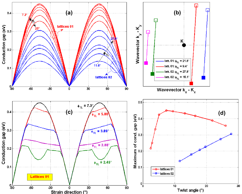
In the regime of small , we find as shown in Fig. 4(c) another trend of in the case of lattices 01, i.e., quite surprisingly reduces around when decreasing , compared to the data in Fig. 4(a). This feature can be explained as follows. On the one hand, the strain tends to enlarge the separation of Dirac cones of the two layers in the -axis and hence increases when tuning from to . On the other hand, the first Brillouin zone is small since the periodic cells are large in the lattices of small . As a consequence, the separation of Dirac cones is limited and its behavior can change (i.e., from increasing to decreasing or vice versa) when the Dirac cone of any layer reaches the edge of Brillouin zone. These properties essentially explain the sudden change of shown in Fig. 4(c). In the situation where the Dirac cones of only one layer can reach the edge of Brillouin zone when tuning , we obtain as shown for , and . For smaller , the Dirac cones of both layers can sequentially reach the edge of Brillouin zone, we additionally observe the valleys of around , i.e., see the data for in Fig. 4(c). Note that, in the case of lattices 02, because both the maximum separation of Dirac cones induced by strain and the size of Brillouin zone tend to reduce when decreasing , the feature discussed here does not occur. The evolution of maximum values of when changing is summarized in Fig. 4(d). When decreasing , the maximum value of decreases monotonically for lattices 02 while it has a peak but also tends to zero for lattices 01. On this basis, it is suggested that to safely achieve a finite conduction gap without requiring the good control of twist angle, designing devices with around/close to should be a good option.
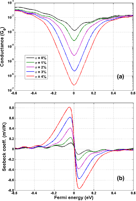
Now, we would like to discuss some possible applications for this type of heterochannels. First, the devices can be used to improve the performance of graphene transistors with the advantage of utilizing a uniform strain and graphene materials only, compared to the strain hetero-channels hung14a and vertical devices brit12 previously studied. Indeed, as shown in Fig. 5(a), with a significant conduction gap, these devices can exhibit a very high ON/OFF current ratio, i.e., up to a few ten thousands for a small strain of only . Second, based on the strong sensitivity of conduction gap to a small strain and its applied direction, this type of devices could be an elementary component of strain sensors. Third, the opening of a finite conduction gap also provides the possibility of enhancing the thermoelectric properties of these devices by strain. As seen in Fig. 5(b), the Seebeck coefficient can reach high values of 600 to 800 V/K for a strain of while it is only about a few tens of V/K in the unstrained case or in the pristine graphene zuev09 . This improvement may be significant for applications as thermal sensors herw86 . Additionally, although our calculations show that the power factor is still limited and hence the thermoelectric figure of merit is small, the phonon conductance is low in this type of devices and one can expect that can be further improved when including additional energy-gap engineering techniques, e.g., by creating a nanohole lattice in graphene layers as suggested in hung14b .
Finally, we would like to make some additional remarks. First, in this kind of devices, the overlap region between the two layers can have important effects on the transport properties. As in the study on vertical structures with Bernal stacking hung14b , the size of this region determines, on the one hand, the coupling strength between layers and, on the other hand, the confinement effects (i.e., see in Fig. 2) because the electronic structure in the bilayer region is very different from that of left and right monolayer graphene sections. However, our calculations show that the change in the size of this overlap region does not dramatically change the ON-current (i.e., beyond the gap) except it can give rise to peaks and shallow valleys in the conductance as seen in Fig. 5. Second, we would like to notice that besides the use of a uniform strain, the vertical devices studied here have the additional advantage of being able to achieve the same values of conduction gap as the unstrained/strained graphene junctions in chun14 , but with smaller strain. For instance, a strain of 4 is enough to achieve a conduction gap of 500 meV while a strain of 67 is required in the latter channels. This improvement comes from the fact that the Dirac cones are displaced by strain in both left and right graphene sections, while in strained/unstrained junctions, the displacement of Dirac cones occurs only in the strained graphene section. Similar improvement can be achieved in the channels made of different strained graphene lattices, e.g., compressive/tensile strained junctions chun14 . However, the control of this complicated strain profile may be a practical issue. Third, besides the case of uniform strains studied here, similar effects can still be obtained in these devices if the strain is applied to only one layer or two different strains to two layers choi10 . In such cases, the properties of should be, of course, strongly dependent on the strain configurations.
In conclusion, we have investigated effects of uniaxial strain on the transport properties of vertical devices made of two twisted graphene layers. It was shown that strain can induce the displacement of Dirac cones of both layers and because of their different orientations, these Dirac cones can be separated in the -space. As a consequence, the device channel can be tuned from metallic to semiconducting by strain. A conduction gap larger than 500 meV can be achieved in the device with a small strain of only 4. The dependence of this conduction gap on the strain strength, strain direction, transport direction and twist angle has been clarified. The twist angle is the good option for a large conduction gap, which is less sensitive to the different types of twisted layers. On this basis, an ON/OFF current ratio as high as a few ten thousands and a strong improvement of Seebeck coefficient can be achieved. The study has hence demonstrated that these vertical devices are very promising for enlarging the applications of graphene in transistors, strain sensors and thermoelectric devices.
Acknowledgment. This research in Hanoi is funded by Vietnam’s National Foundation for Science and Technology Development (NAFOSTED) under grant number 103.01-2014.24.
References
- (1) A. H. Castro Neto, F. Guinea, N. M. R. Peres, K. S. Novoselov, and A. K. Geim, Rev. Mod. Phys. 81, 109 (2009).
- (2) Y. Wu, D. B. Farmer, F. Xia, and P. Avouris, Proc. IEEE 101, 1620 (2013).
- (3) O. V. Yazyev, Rep. Prog. Phys. 73, 056501 (2010).
- (4) A. A. Balandin, Nat. Mater. 10, 569 (2011).
- (5) B. K. Sharma and J.-H. Ahn, Solid State Electron. 89, 177 (2013).
- (6) K. S. Novoselov, V. I. Fal’ko, L. Colombo, P. R. Gellert, M. G. Schwab, and K. Kim, Nature 490, 192 (2012).
- (7) F. Schwierz, Nat. Nanotechnol. 5, 487 (2010).
- (8) I. Meric, M. Y. Han, A. F. Young, B. Özyilmaz, P. Kim, and K. L. Shepard, nat. Nanotechnol. 3, 654 (2008).
- (9) M. Y. Han, B. Özyilmaz, Y. Zhang, and P. Kim, Phys. Rev. Lett. 98, 206805 (2007).
- (10) N. Kharche and S. K. Nayak, Nano Lett. 11, 5274 (2011); S. Tang et al., Sci. Rep. 3, 2666 (2013).
- (11) A. Lherbier et al., Nano Lett. 13, 1446 (2013); A. Zabet-Khosousi et al., J. Am. Chem. Soc. 136, 1391 (2014).
- (12) Y. Zhang, T.-T. Tang, C. Girit, Z. Hao, M. C. Martin, A. Zettl, M. F. Crommie, Y. R. Shen, and F. Wang, Nature 459, 820 (2009).
- (13) J. Bai, X. Zhong, S. Jiang, Y. Huang, and X. Duan, Nat. Nanotechnol. 5, 190 (2010).
- (14) G. Fiori, A. Betti, S. Bruzzone, and G. Iannaccone, ACS Nano 6, 2642 (2012).
- (15) L. Britnell et al., Science 335, 947 (2012); L. Britnell et al., Nat. Commun. 4, 1794 (2013); W. J. Yu et al., Nat. Nanotechnol. 8, 952 (2013).
- (16) H. H. P. Garza, E. W. Kievit, G. F. Schneider, and U. Staufer, Nano Lett. 14, 4107 (2014).
- (17) H. Shioya, M. F. Craciun, S. Russo, M. Yamamoto, and S. Tarucha, Nano Lett. 14, 1158 (2014).
- (18) V. M. Pereira and A. H. Castro Neto, Phys. Rev. Lett. 103, 046801 (2009).
- (19) V. M. Pereira, A. H. Castro Neto, and N. M. R. Peres, Phys. Rev. B 80, 045401 (2009).
- (20) G. Cocco, E. Cadelano, and L. Colombo, Phys. Rev. B 81, 241412 (2010).
- (21) Y. Lu and J. Guo, Appl. Phys. Lett. 97, 073105 (2010).
- (22) S. Bala Kumar and Jing Guo, Nano Lett. 12, 1362 (2012).
- (23) D. A. Bahamon and Vitor M. Pereira, Phys. Rev. B 88, 195416 (2013).
- (24) V. Hung Nguyen, H. Viet Nguyen, and P. Dollfus, Nanotechnol. 25, 165201 (2014).
- (25) M. Chung Nguyen, V. Hung Nguyen, H. Viet Nguyen, and P. Dollfus, Semicond. Sci. Technol. 29, 115024 (2014).
- (26) V. M. Pereira, R. M. Ribeiro, N. M. R. Peres, and A. H. Castro Neto, Europhys. Lett. 92, 67001 (2010).
- (27) G.-X. Ni, H.-Z. Yang, W. Ji, S.-J. Baeck, C.-T. Toh, J.-H. Ahn, V. M. Pereira, and B. Özyilmaz, Adv. Mater. 26, 1081 (2014).
- (28) F. Guinea, M. I. Katsnelson, and A. K. Geim, Nat. Phys. 6, 30 (2010).
- (29) T. Low and F. Guinea, Nano Lett. 10, 3551 (2010).
- (30) F. Zhai and L. Yang, Appl. Phys. Lett. 98, 062101 (2011).
- (31) W. A. de Heer, C. Berger, X. Wu, P. N. First, E. H. Conrad, X. Li, T. Li, M. Sprinkle, J. Hass, M. L. Sadowski, M. Potemski, G. Martinez, Solid State Commun. 143, 92 (2007).
- (32) J. Hass, F. Varchon, J. E. Millan-Otoya, M. Sprinkle, N. Sharma, W. A. de Heer, C. Berger, P. N. First, L. Magaud, and E. H. Conrad, Phys. Rev. Lett. 100, 125504 (2008).
- (33) V. Carozo, C. M. Almeida, E. H. M. Ferreira, L. G. Cancado, C. A. Achete, and A. Jorio, Nano Lett. 11, 4527 (2011).
- (34) A. Luican, G. Li, A. Reina, J. Kong, R. R. Nair, K. S. Novoselov, A. K. Geim, and E. Y. Andrei, Phys. Rev. Lett. 106, 126802 (2011).
- (35) R. W. Havener, H. Zhuang, L. Brown, R. G. Hennig, and J. Park, Nano Lett. 12, 3162 (2012).
- (36) C.-C. Lu, Y.-C. Lin, Z. Liu, C.-H. Yeh, K. Suenaga, and P.-W. Chiu, ACS Nano 7, 2587 (2013).
- (37) J. M. B. Lopes dos Santos, N. M. R. Peres, and A. H. Castro Neto, Phys. Rev. Lett. 99, 256802 (2007).
- (38) G. Trambly de Laissardière, D. Mayou, and L. Magaud, Nano Lett. 10, 804 (2010).
- (39) Guohong Li, A. Luican, J. M. B. Lopes dos Santos, A. H. Castro Neto, A. Reina, J. Kong, and E. Y. Andrei, Nat. Phys. 6, 109 (2010).
- (40) A. I. Cocemasov, D. L. Nika, and A. A. Balandin, Phys. Rev. B 88, 035428 (2013); Apl. Phys. Lett. 105, 031904 (2014).
- (41) J. M. B. Lopes dos Santos, N. M. R. Peres, and A. H. Castro Neto, Phys. Rev. B 86, 155449 (2012).
- (42) V. Hung Nguyen, M. Chung Nguyen, H. Viet Nguyen, J. Saint-Martin, and P. Dollfus, Appl. Phys. Lett. 105, 133105 (2014).
- (43) O. L. Blakslee, D. G. Proctor, E. J. Seldin, G. B. Spence, and T. Weng, J. Appl. Phys. 41, 3373 (1970).
- (44) Y. M. Zuev, W. Chang, and P. Kim, Phys. Rev. Lett. 102, 096807 (2009).
- (45) A. W. Van Herwaarden and P. Sarro, Sens. Actuators 10, 321 (1986).
- (46) S.-M. Choi, S.-H. Jhi, and T.-W. Son, Nano Lett. 10, 3486 (2010).